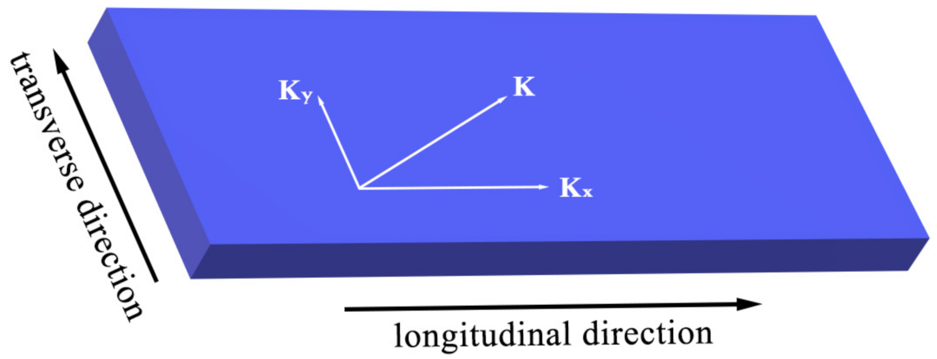
2.1. Two-Dimensional Coupling-of-Modes Equations
The 1-D COM theory was based on the plane-wave assumption that ignored the diffraction phenomenon in the propagation of the SAW. Thus, it can’t simulate the transverse mode of the device. In the 2-D COM theory, the surface acoustic wave is no longer approximated to a plane wave whose wave vector
K is decomposed into two orthogonal components
Kx and
Ky, corresponding to the longitudinal and transverse components of the device, respectively, as shown in
Figure 2.
According to the slowness curve of the SAW on piezoelectric substrate, the relationship between wave vector component
Kx and
Ky will be established approximately. The parabola approximate form [
14] was shown in Equation (1). And the biquadratic approximate form [
6] was shown in Equation (2).
Here, , , are the parameters to characterize the anisotropy of piezoelectric substrate; is the wave number according to the electric period of the IDT.
Based on the 1-D COM equation and the slowness relation of the SAW, the 2-D COM equation can be obtained. As shown in Equation (3), the 2-D COM equations in the form of biquadratic approximation is adopted in this paper.
Here, , are the particle displacements of waves propagating forward and backward directions, respectively; , , , and represent coupling coefficient, excitation coefficient, static capacitance, input voltage and output current.
2.3. Two-Dimensional COM Parameters
The 2-D COM parameters are composed of the 1-D COM parameters
v,
κ,
α,
C and the anisotropic parameters
,
. The 1-D COM parameters can be determined by Equation (4).
Here, , , , and denote the up and down boundary frequency of the stop band in periodic shorted grating and open grating; , and represent the input voltage, the acoustic aperture and the electrostatic energy.
To determine
,
,
,
and
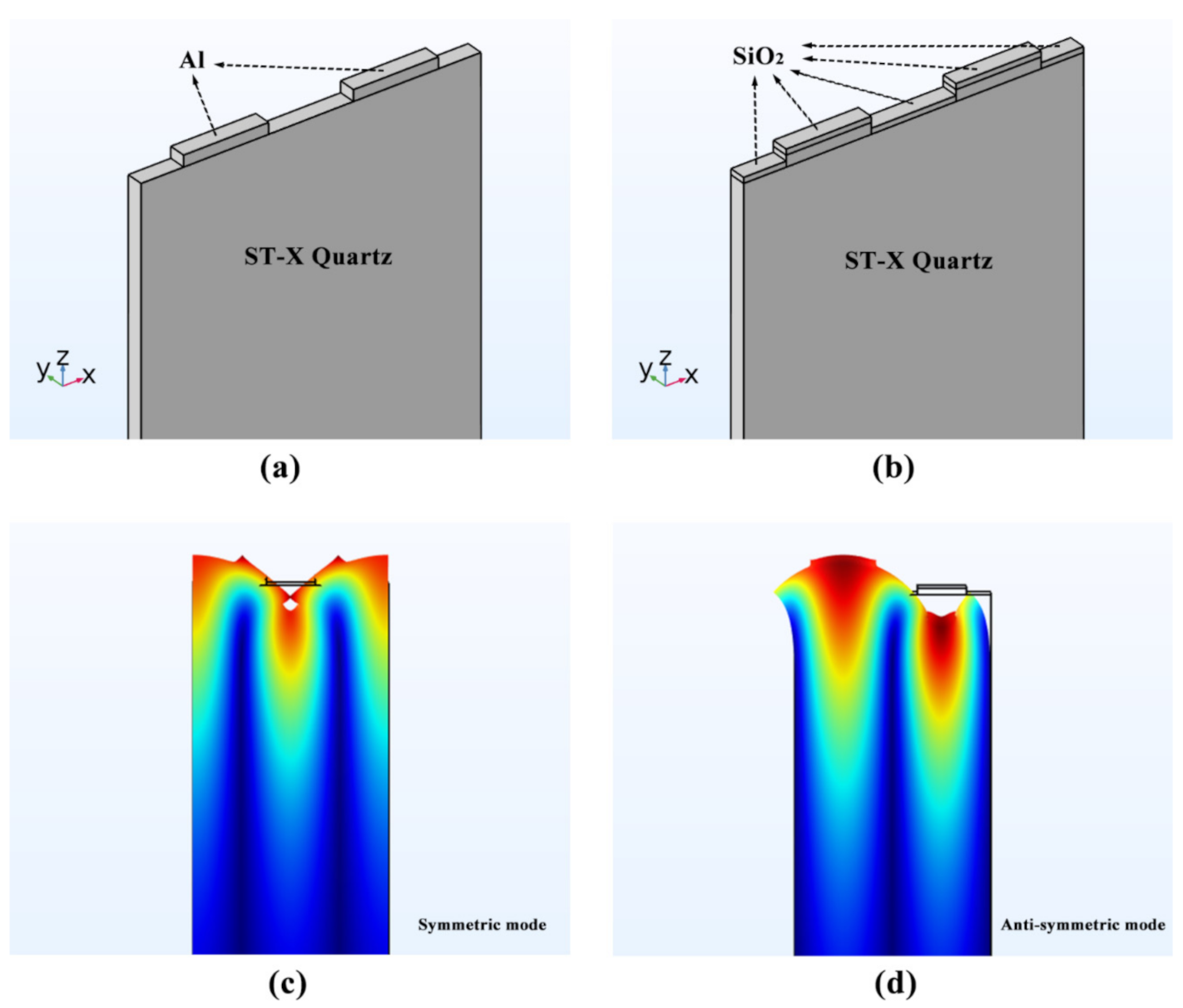
, a 3D periodic finite element model, including a pair of IDTs, was established as shown in
Figure 5. And the substrate material and structural parameters of the model were given in
Table 2.
By setting the boundary conditions of constant voltage or constant charge electrode, the periodic grating was controlled to be shorted grating and open grating. The resonant frequencies of symmetric and anti-symmetric Rayleigh surface acoustic wave (R-SAW) modes corresponding to the up and down boundary frequency of the stop band.
By performing static analysis in the FEM software (COMSOL Multiphysics), the electrostatic energy of the periodic element can be obtained.
The 1-D COM parameters of IDTs with and without mass loading were calculated by Equation (4), as shown in
Table 3.
By calculating the second and fourth derivatives at the zero point of the slowness curve, the anisotropic parameters were obtained [
6].
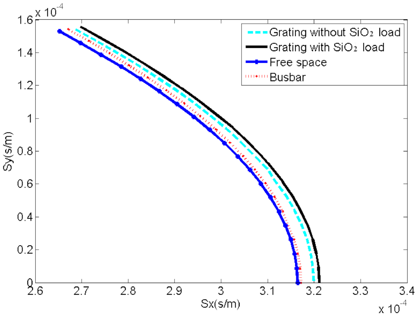
To obtain the slowness curves of the SAW, the periodic conditions of the 3D periodic FEM model at the front and back side should be set up to a Floquet-Bloch boundary conditions form as follows:
Here, and denote the wave amplitudes at front side and back side, and is the oblique angle.
By calculating the slowness of the SAW with different oblique angles, the slowness curves were obtained.
The slowness curves of the SAW in different domains on ST-X quartz substrate were shown in
Figure 6.
The anisotropic parameters
and
of each domain were obtained by Equations (5) and (6), as shown in
Table 4.
2.5. Admittance Matrix and Insertion Loss
For the two-port SAW resonator, the relationship between the output current
I and the input voltage
V was given by Equation (11):
Here, Y matrix was the admittance matrix of the device.
The current of each port was obtained by Equation (12):
By short-circuiting the IDTs of the two ports respectively and calculating the current of each port, the admittance matrix was obtained.
The principle of the short-circuiting operation to calculate the admittance matrix’s elements was summarized in
Table 5.
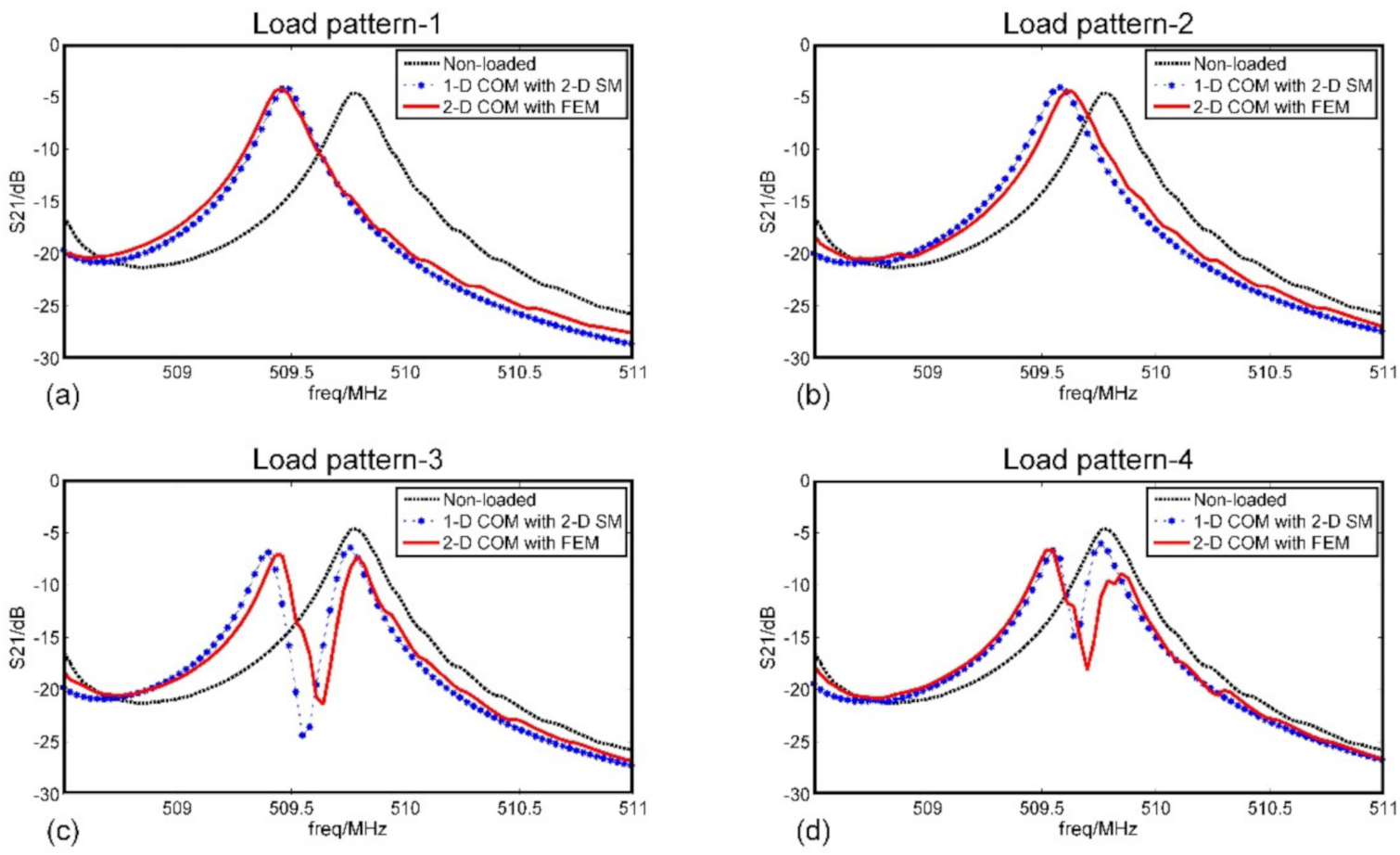
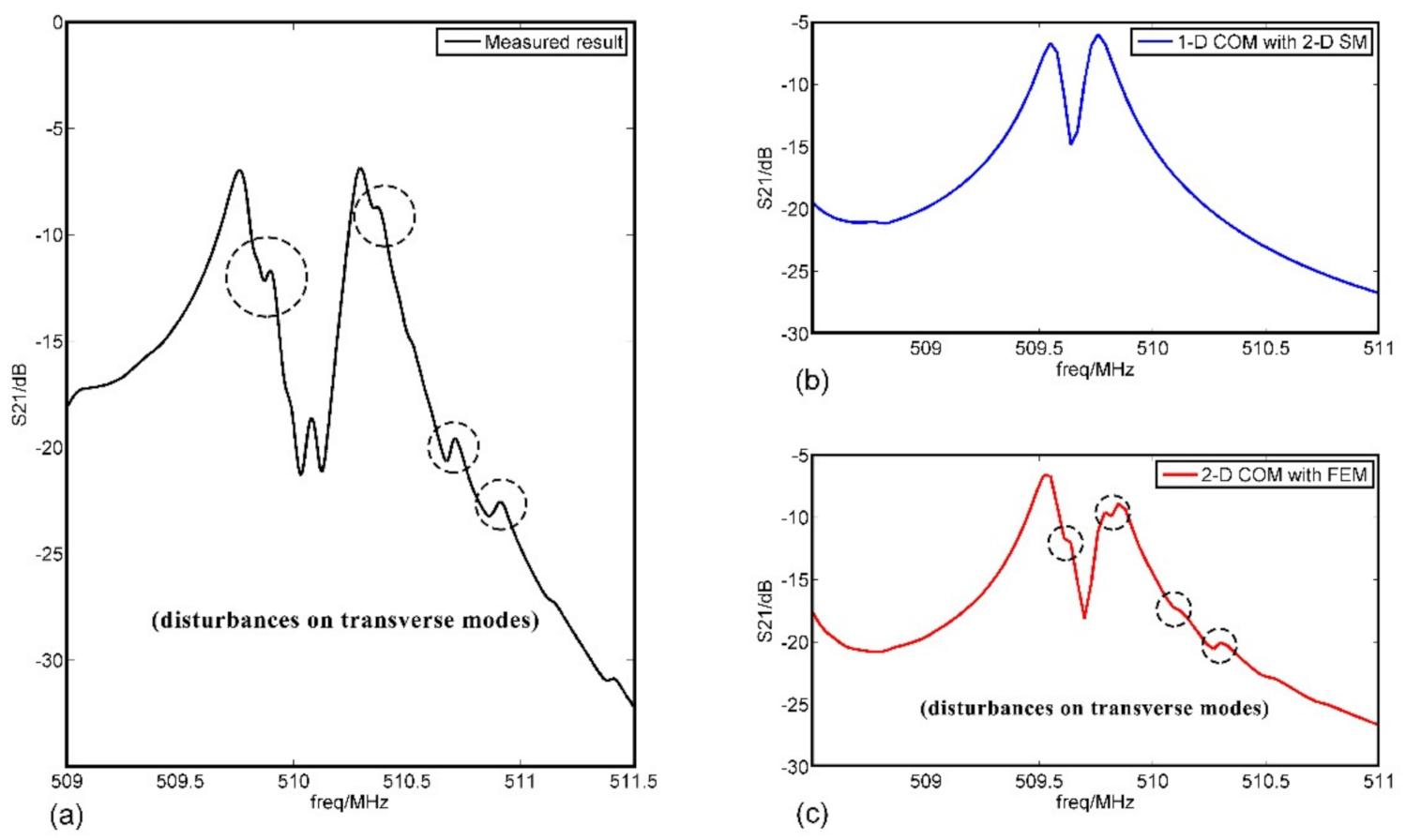
In this paper, the insertion loss (S
21) parameter of SAW resonator was chosen as the response signal of the sensor. The relationship between the insertion loss (S
21) and the admittance matrix is given by Equation (13):
where
Y01,
Y02 denote transmission admittance.
2.6. Experimental Design
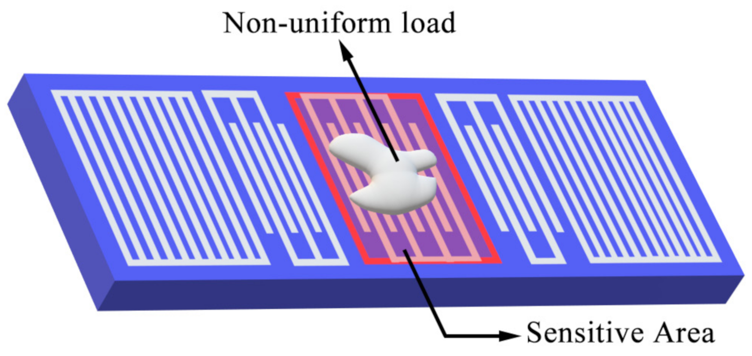
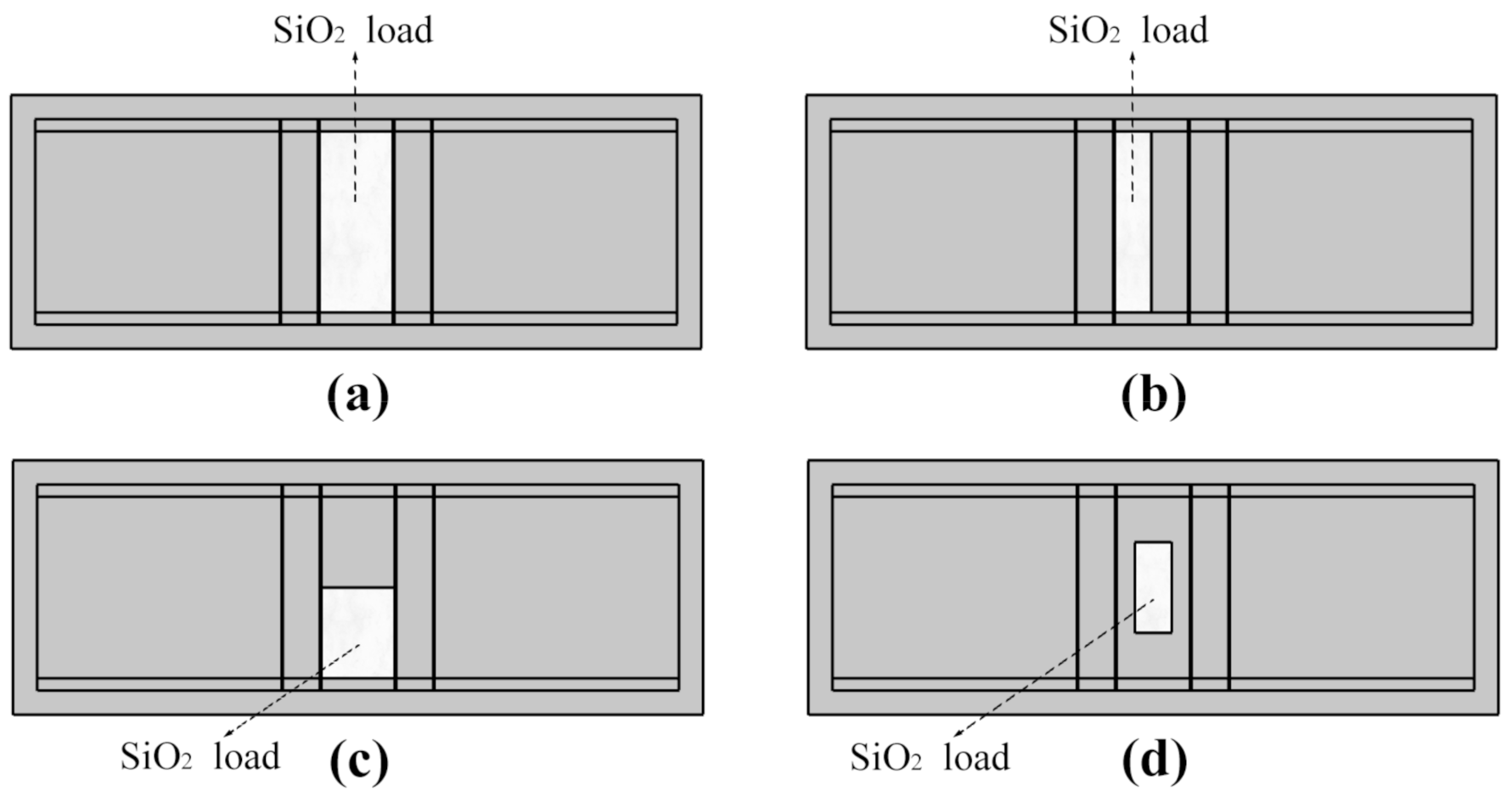
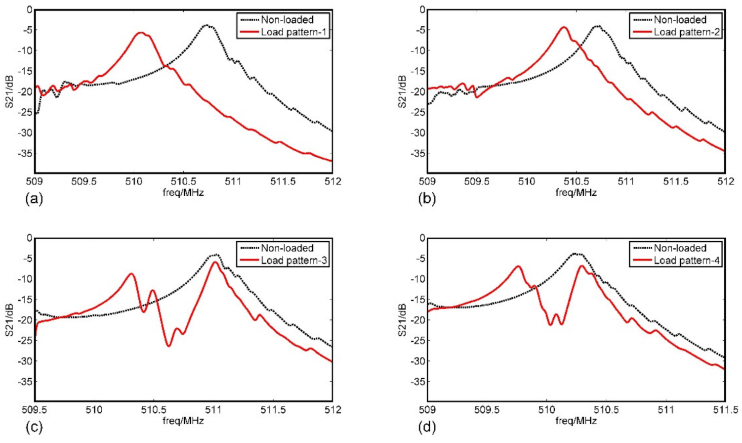
Using SiO2 as the loading material, we fabricated a series of SAW resonators with the loads in four distribution patterns. The fabrication process was as follows:
Firstly, metallic materials Al was deposited on the ST-X quartz substrate with a thickness of 2000 Å using an electron beam evaporator. Secondly, the photoresist (PR) was spin-coated, exposed and patterned for gratings. Thirdly, the Al was wet-etched and the PR was dissolved in acetone and the SAW resonators without SiO2 layers were fabricated. Finally, the SiO2 was deposited at 4 different distributions with a photomask we designed by using overlay technology, and the SAW resonators with the loads in four patterns were fabricated.
The photos of the SAW resonators under 4 different load patterns were taken by a microscope (LEICA DM4 M), as shown in
Figure 7a–d. The information of material and structural parameters in the experiment was summarized in
Table 6.
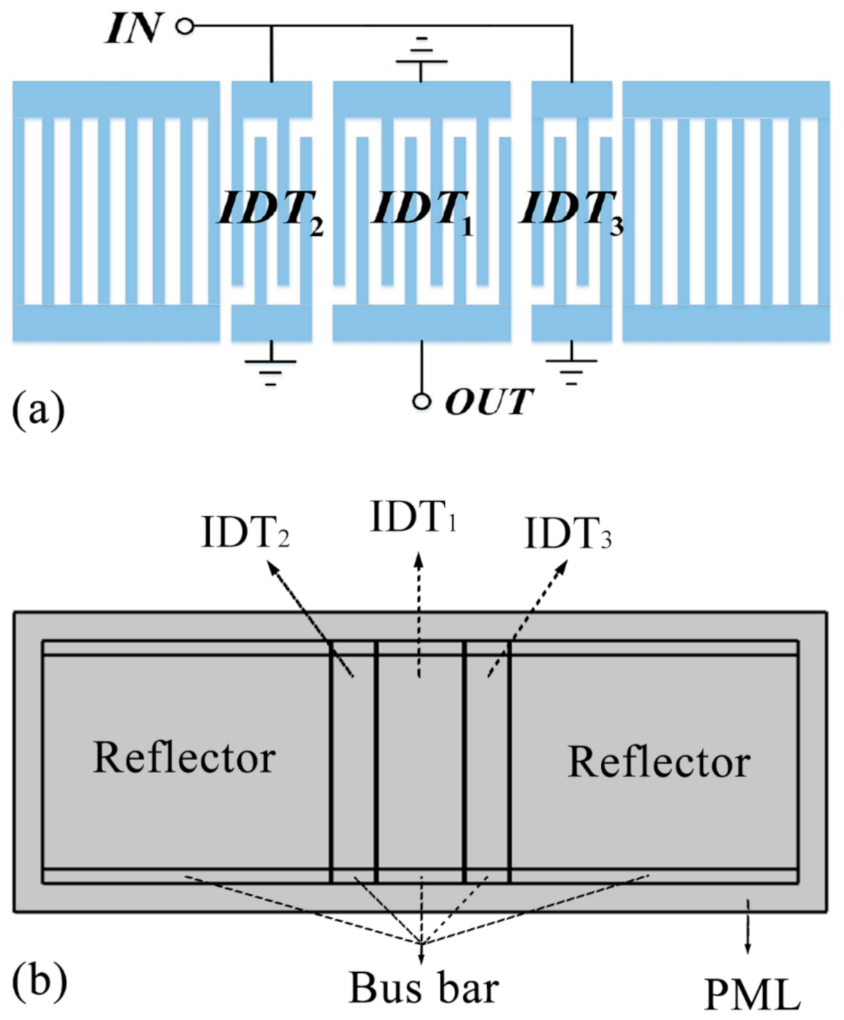
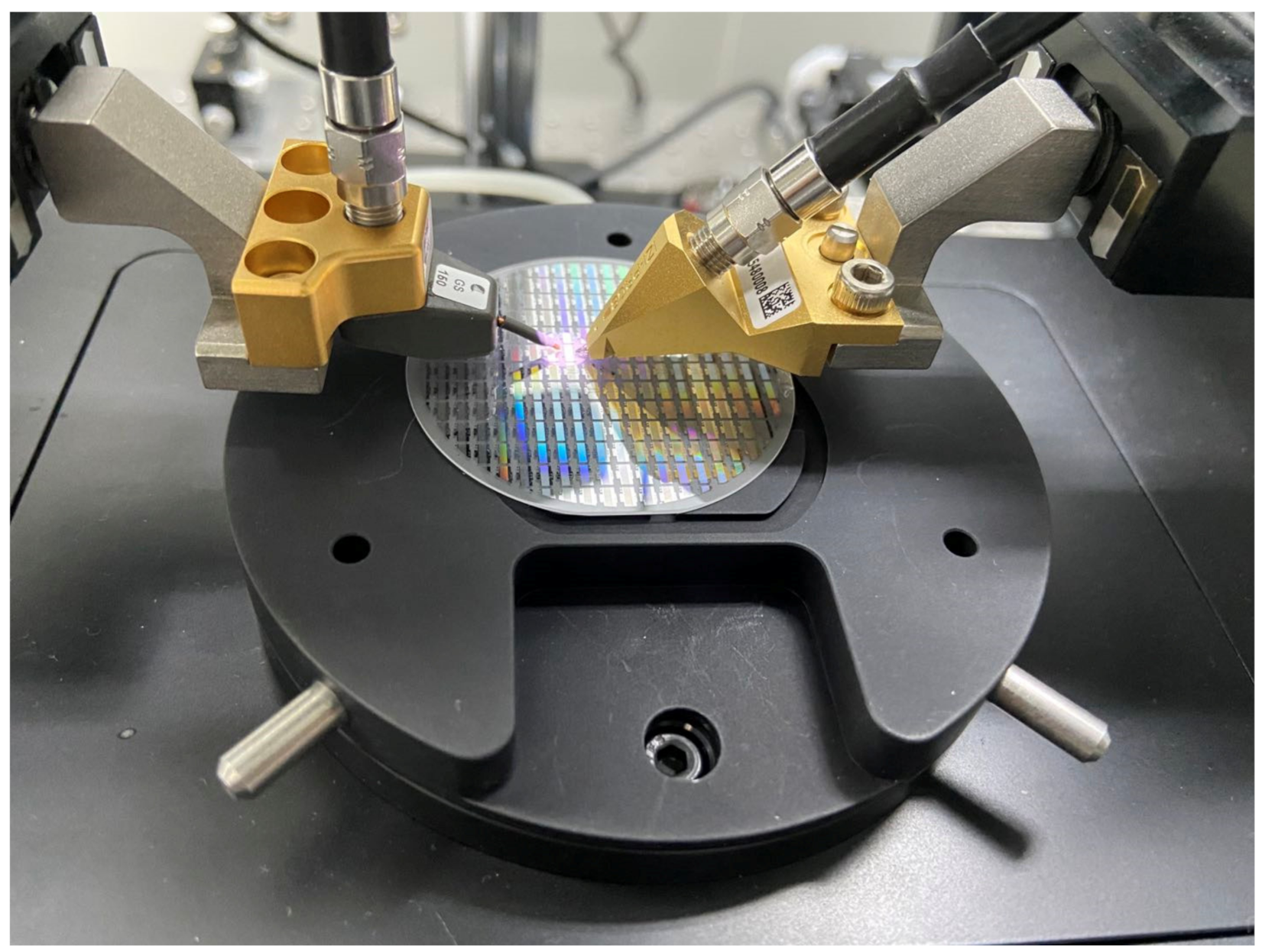
In the experiment the input port (IDT 2, IDT 3) and output port (IDT1) were connected to the VNA (Agilent E5071B Network analyzer) by using a probe device, which was shown in
Figure 8.


