Surface Potential/Charge Sensing Techniques and Applications


Abstract
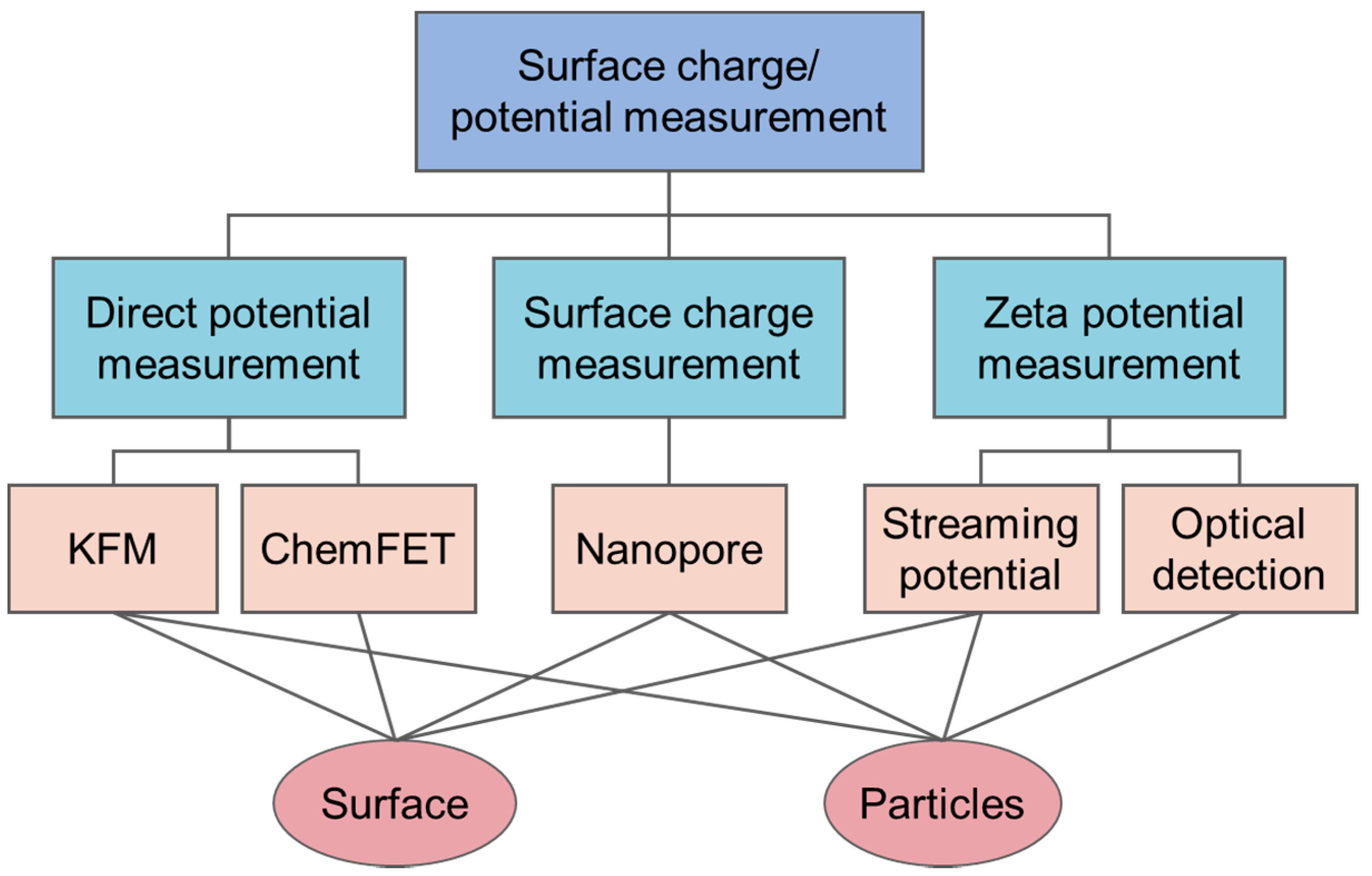
:1. Introduction
2. Direct Surface Potential Measurement
2.1. Kelvin Probe Force Microscopy (KFM)
2.2. Chemical Field Effect Transistor (ChemFET)-Based Potential Sensing
3. Surface Charge Measurement
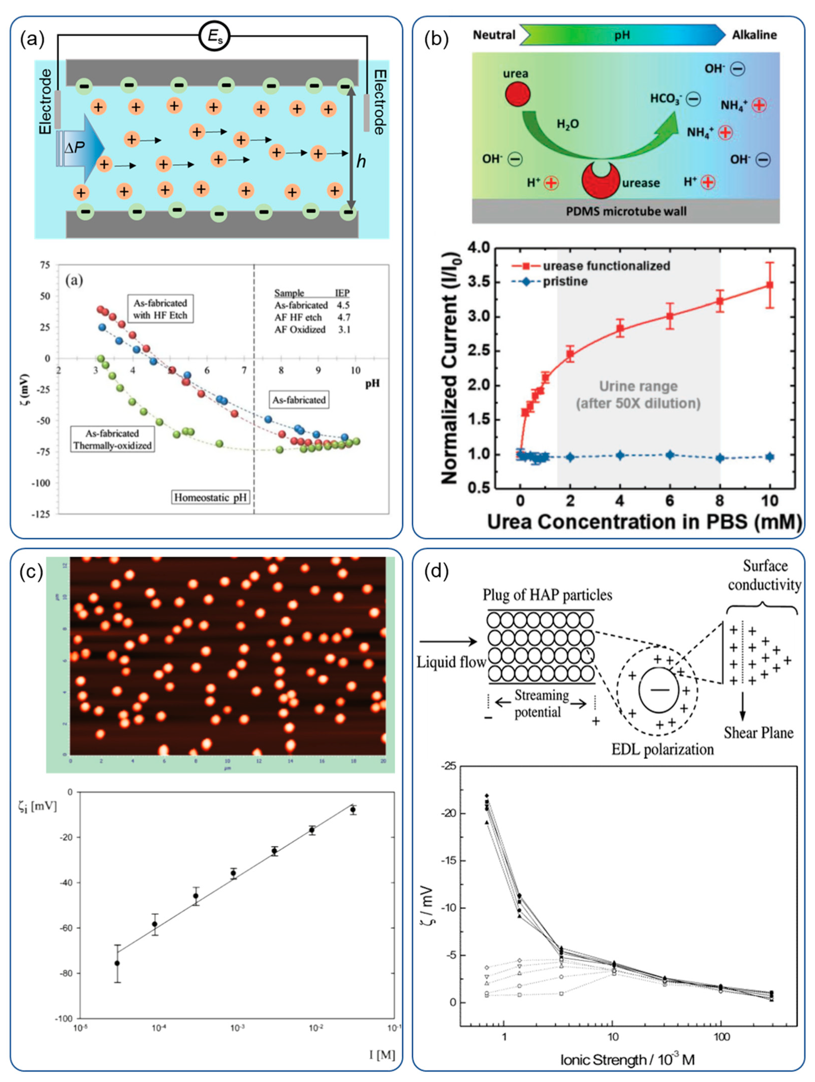
4. Zeta Potential Measurement
4.1. Streaming Potential Measurement
4.2. Optical Detection
5. Conclusions and Outlook
Author Contributions
Funding
Conflicts of Interest
References
- Fu, W.; Jiang, L.; Van Geest, E.P.; Schneider, G.F.; Schneider, G.F. Sensing at the Surface of Graphene Field-Effect Transistors. Adv. Mater. 2016, 29, 1603610. [Google Scholar] [CrossRef] [PubMed] [Green Version]
- Chen, S.; Tang, Y.; Zhan, K.; Sun, D.; Hou, X. Chemiresistive nanosensors with convex/concave structures. Nano Today 2018, 20, 84–100. [Google Scholar] [CrossRef]
- Li, Y.; Lai, S.N.; Zheng, B. A microfluidic streaming potential analyzer for label-free DNA detection. Sens. Actuators B Chem. 2018, 259, 871–877. [Google Scholar] [CrossRef]
- Chen, F.; Huang, H.; Guo, L.; Zhang, Y.; Ma, T. The Role of Polarization in Photocatalysis. Angew. Chem. Int. Ed. 2019, 58, 10061–10073. [Google Scholar] [CrossRef]
- Takadoum, J. The influence of potential on the tribocorrosion of nickel and iron in sulfuric acid solution. Corros. Sci. 1996, 38, 643–654. [Google Scholar] [CrossRef]
- Nordt, F.J. Alterations in surface charge density versus changes in surface charge topography in aging red blood cells. Ann. Hematol. 1980, 40, 233–238. [Google Scholar] [CrossRef]
- Kirby, B.; Wheeler, A.R.; Zare, R.N.; Fruetel, J.A.; Shepodd, T.J. Programmable modification of cell adhesion and zeta potential in silica microchips. Lab Chip 2003, 3, 5–10. [Google Scholar] [CrossRef]
- Zhu, X.; Mason, T.G. Separating Nanoparticles by Surface Charge Group Using pH-Controlled Passivated Gel Electrophoresis. Soft Mater. 2016, 14, 204–209. [Google Scholar] [CrossRef]
- Chen, S.-L.; Wang, S.; Lucia, L.A. New insights into the fundamental nature of lignocellulosic fiber surface charge. J. Colloid Interface Sci. 2004, 275, 392–397. [Google Scholar] [CrossRef]
- Salvo, P.; Melai, B.; Calisi, N.; Paoletti, C.; Bellagambi, F.G.; Kirchhain, A.; Trivella, M.; Fuoco, R.; Di Francesco, F. Graphene-based devices for measuring pH. Sens. Actuators B Chem. 2018, 256, 976–991. [Google Scholar] [CrossRef]
- Ma, Y.; Yeh, L.-H.; Qian, S. pH-regulated ionic conductance in a nanopore. Electrochem. Commun. 2014, 43, 91–94. [Google Scholar] [CrossRef]
- Cui, Y.; Wei, Q.; Park, H.; Lieber, C.M. Nanowire Nanosensors for Highly Sensitive and Selective Detection of Biological and Chemical Species. Science 2001, 293, 1289–1292. [Google Scholar] [CrossRef] [PubMed]
- Lin, C.-Y.; Acar, E.T.; Polster, J.W.; Lin, K.; Hsu, J.-P.; Siwy, Z.S. Modulation of Charge Density and Charge Polarity of Nanopore Wall by Salt Gradient and Voltage. ACS Nano 2019, 13, 9868–9879. [Google Scholar] [CrossRef] [PubMed]
- Chen, S.; Van Nieuwkasteele, J.W.; Berg, A.V.D.; Eijkel, J. Ion-Step Method for Surface Potential Sensing of Silicon Nanowires. Anal. Chem. 2016, 88, 7890–7893. [Google Scholar] [CrossRef] [Green Version]
- Kurkina, T.; Vlandas, A.; Ahmad, A.; Kern, K.; Balasubramanian, K. Label-Free Detection of Few Copies of DNA with Carbon Nanotube Impedance Biosensors. Angew. Chem. Int. Ed. 2011, 50, 3710–3714. [Google Scholar] [CrossRef]
- Adam, T.; Hashim, U. Highly sensitive silicon nanowire biosensor with novel liquid gate control for detection of specific single-stranded DNA molecules. Biosens. Bioelectron. 2015, 67, 656–661. [Google Scholar] [CrossRef]
- Chiesa, M.; Cardenas, P.; Otón, F.; Martínez, J.; Mas-Torrent, M.; Garcia, F.; Alonso, J.C.; Rovira, C.; Garcia, R. Detection of the Early Stage of Recombinational DNA Repair by Silicon Nanowire Transistors. Nano Lett. 2012, 12, 1275–1281. [Google Scholar] [CrossRef]
- Duan, X.; Li, Y.; Rajan, N.K.; Routenberg, D.A.; Modis, Y.; Reed, M. Quantification of the affinities and kinetics of protein interactions using silicon nanowire biosensors. Nat. Nanotechnol. 2012, 7, 401–407. [Google Scholar] [CrossRef]
- Chen, S.; Xie, Y.; De, A.; Berg, A.V.D.; Carlen, E.T. Electrical shielding for silicon nanowire biosensor in microchannels. Appl. Phys. Lett. 2013, 103, 173702. [Google Scholar] [CrossRef] [Green Version]
- Kim, D.R.; Lee, C.H.; Zheng, X. Probing Flow Velocity with Silicon Nanowire Sensors. Nano Lett. 2009, 9, 1984–1988. [Google Scholar] [CrossRef]
- Nonnenmacher, M.; O’Boyle, M.P.; Wickramasinghe, H. Kelvin probe force microscopy. Appl. Phys. Lett. 1991, 58, 2921–2923. [Google Scholar] [CrossRef] [Green Version]
- Melitz, W.; Shen, J.; Kummel, A.; Lee, S. Kelvin probe force microscopy and its application. Surf. Sci. Rep. 2011, 66, 1–27. [Google Scholar] [CrossRef]
- Arai, T.; Tomitori, M. Observation of electronic states on Si(111)-(7 × 7) through short-range attractive force with noncontact atomic force spectroscopy. Phys. Rev. Lett. 2004, 93, 256101. [Google Scholar] [CrossRef] [PubMed] [Green Version]
- Okamoto, K.; Yoshimoto, K.; Sugawara, Y.; Morita, S. KPFM imaging of Si(1 1 1) 53 × 53 sb surface for atom distinction using NC-AFM. Appl. Surf. Sci. 2003, 210, 128–133. [Google Scholar] [CrossRef]
- Shiota, T.; Nakayama, K. Atom-resolved imaging of the potential distribution at Si (111) 7 × 7 surfaces. Jpn. J. Appl. Phys. 2002, 41, L1178–L1180. [Google Scholar] [CrossRef]
- Enevoldsen, G.H.; Glatzel, T.; Christensen, M.C.; Lauritsen, J.V.; Besenbacher, F. Atomic Scale Kelvin Probe Force Microscopy Studies of the Surface Potential Variations on the TiO2(110) Surface. Phys. Rev. Lett. 2008, 100, 236104. [Google Scholar] [CrossRef]
- Hoppe, H.; Glatzel, T.; Niggemann, M.; Hinsch, A.; Lux-Steiner, M.C.; Sariciftci, N.S. Kelvin Probe Force Microscopy Study on Conjugated Polymer/Fullerene Bulk Heterojunction Organic Solar Cells. Nano Lett. 2005, 5, 269–274. [Google Scholar] [CrossRef]
- Hallam, T.; Duffy, C.M.; Minakata, T.; Ando, M.; Sirringhaus, H. A scanning Kelvin probe study of charge trapping in zone-cast pentacene thin film transistors. Nanotechnology 2008, 20, 025203. [Google Scholar] [CrossRef]
- Clack, N.G.; Salaita, K.; Groves, J.T. Electrostatic readout of DNA microarrays with charged microspheres. Nat. Biotechnol. 2008, 26, 825–830. [Google Scholar] [CrossRef] [Green Version]
- Stone, A.D.D.; Mesquida, P. Kelvin-probe force microscopy of the pH-dependent charge of functional groups. Appl. Phys. Lett. 2016, 108, 233702. [Google Scholar] [CrossRef] [Green Version]
- García, R.; Garcia, R.; Pérez, R. Dynamic atomic force microscopy methods. Surf. Sci. Rep. 2002, 47, 197–301. [Google Scholar] [CrossRef]
- Albrecht, T.R.; Horne, D.; Rugar, D.; Grütter, P. Frequency modulation detection using high-Q cantilevers for enhanced force microscope sensitivity. J. Appl. Phys. 1991, 69, 668–673. [Google Scholar] [CrossRef] [Green Version]
- Ozasa, K.; Nemoto, S.; Maeda, M.; Hara, M. Kelvin probe force microscope with near-field photoexcitation. J. Appl. Phys. 2010, 107, 103501. [Google Scholar] [CrossRef]
- Cohen, G.; Halpern, E.; Nanayakkara, S.U.; Luther, J.M.; Held, C.; Bennewitz, R.; Boag, A.; Rosenwaks, Y. Reconstruction of surface potential from Kelvin probe force microscopy images. Nanotechnology 2013, 24, 295702. [Google Scholar] [CrossRef] [PubMed]
- Park, J.; Yang, J.; Lee, G.; Lee, C.Y.; Na, S.; Lee, S.W.; Haam, S.; Huh, Y.-M.; Yoon, D.S.; Eom, K.; et al. Single-Molecule Recognition of Biomolecular Interaction via Kelvin Probe Force Microscopy. ACS Nano 2011, 5, 6981–6990. [Google Scholar] [CrossRef]
- Jang, K.; Choi, J.; Park, C.; Na, S. Label-free and high-sensitive detection of Kirsten rat sarcoma viral oncogene homolog and epidermal growth factor receptor mutation using Kelvin probe force microscopy. Biosens. Bioelectron. 2017, 87, 222–228. [Google Scholar] [CrossRef]
- Leung, C.; Kinns, H.; Hoogenboom, B.W.; Howorka, S.; Mesquida, P. Imaging Surface Charges of Individual Biomolecules. Nano Lett. 2009, 9, 2769–2773. [Google Scholar] [CrossRef]
- Park, C.; Jang, K.; Lee, S.; You, J.; Lee, S.; Ha, H.; Yun, K.; Kim, J.; Lee, H.; Park, J.; et al. A highly sensitive, direct and label-free technique for Hg2+ detection using Kelvin probe force microscopy. Nanotechnology 2015, 26, 305501. [Google Scholar] [CrossRef]
- Park, J.; Lee, S.; Jang, K.; Na, S. Ultra-sensitive direct detection of silver ions via Kelvin probe force microscopy. Biosens. Bioelectron. 2014, 60, 299–304. [Google Scholar] [CrossRef]
- Kim, W.; Lee, G.; Kim, M.; Park, J.; Jo, S.; Yoon, D.S.; Park, Y.H.; Hong, J.; Park, J. Al3+ ion sensing at attomole level via surface-potential mapping of gold nanoparticle complexes. Sens. Actuators B Chem. 2018, 255, 2179–2186. [Google Scholar] [CrossRef]
- Luth, H. Solid Surfaces, Interfaces and Thin Films, 5th ed.; Springer: Berlin, Germany, 2010. [Google Scholar]
- Sadewasser, S.; Leendertz, C.; Streicher, F.; Lux-Steiner, M.C. The influence of surface topography on Kelvin probe force microscopy. Nanotechnology 2009, 20, 505503. [Google Scholar] [CrossRef] [PubMed]
- Garcia, R.; Herruzo, E.T. The emergence of multifrequency force microscopy. Nat. Nanotechnol. 2012, 7, 217–226. [Google Scholar] [CrossRef] [PubMed] [Green Version]
- Ding, X.D.; An, J.; Xu, J.-B.; Li, C.; Zeng, R.Y. Improving lateral resolution of electrostatic force microscopy by multifrequency method under ambient conditions. Appl. Phys. Lett. 2009, 94, 223109. [Google Scholar] [CrossRef]
- Stark, R.W.; Naujoks, N.; Stemmer, A. Multifrequency electrostatic force microscopy in the repulsive regime. Nanotechnology 2007, 18, 065502. [Google Scholar] [CrossRef]
- Chen, S.; Bomer, J.G.; Van Der Wiel, W.G.; Carlen, E.T.; Berg, A.V.D. Top-Down Fabrication of Sub-30 nm Monocrystalline Silicon Nanowires Using Conventional Microfabrication. ACS Nano 2009, 3, 3485–3492. [Google Scholar] [CrossRef]
- Elfström, N.; Karlström, A.E.; Linnros, J. Silicon Nanoribbons for Electrical Detection of Biomolecules. Nano Lett. 2008, 8, 945–949. [Google Scholar] [CrossRef]
- Heller, I.; Janssens, A.M.; Männik, J.; Minot, E.D.; Lemay, S.G.; Dekker, C. Identifying the Mechanism of Biosensing with Carbon Nanotube Transistors. Nano Lett. 2008, 8, 591–595. [Google Scholar] [CrossRef]
- Liao, L.; Bai, J.; Cheng, R.; Lin, Y.-C.; Jiang, S.; Huang, Y.; Duan, X. Top-Gated Graphene Nanoribbon Transistors with Ultrathin High-kDielectrics. Nano Lett. 2010, 10, 1917–1921. [Google Scholar] [CrossRef] [Green Version]
- Vankerkhof, J.; Bergveld, P.; Schasfoort, R. The ISFET based heparin sensor with a monolayer of protamine as affinity ligand. Biosens. Bioelectron. 1995, 10, 269–282. [Google Scholar] [CrossRef] [Green Version]
- Chen, S.; Bomer, J.G.; Carlen, E.T.; van den Berg, A. Al2O3/silicon nanoISFET with near ideal Nernstian response. Nano Lett. 2011, 11, 2334–2341. [Google Scholar] [CrossRef]
- Heller, I.; Mannik, J.; Lemay, S.G.; Dekker, C. Optimizing the Signal-to-Noise Ratio for Biosensing with Carbon Nanotube Transistors. Nano Lett. 2009, 9, 377–382. [Google Scholar] [CrossRef] [PubMed]
- Wipf, M.; Stoop, R.L.; Tarasov, A.; Bedner, K.; Fu, W.; Wright, I.A.; Martin, C.J.J.; Constable, E.C.; Calame, M.; Schönenberger, C.; et al. Selective Sodium Sensing with Gold-Coated Silicon Nanowire Field-Effect Transistors in a Differential Setup. ACS Nano 2013, 7, 5978–5983. [Google Scholar] [CrossRef] [PubMed]
- Schasfoort, R.; Bergveld, P.; Kooyman, R.; Greve, J. The ion-step-induced response of membrane-coated ISFETs: Theoretical description and experimental verification. Biosens. Bioelectron. 1991, 6, 477–489. [Google Scholar] [CrossRef] [Green Version]
- Novoselov, K.S.; Geim, A.K.; Morozov, S.V.; Jiang, D.; Katsnelson, M.I.; Grigorieva, I.V.; Dubonos, S.V.; Firsov, A.A. Two-dimensional gas of massless Dirac fermions in graphene. Nature 2005, 438, 197–200. [Google Scholar] [CrossRef]
- Song, S.M.; Park, J.K.; Sul, O.J.; Cho, B.J. Determination of Work Function of Graphene under a Metal Electrode and Its Role in Contact Resistance. Nano Lett. 2012, 12, 3887–3892. [Google Scholar] [CrossRef] [PubMed]
- Bergveld, P. Thirty years of isfetology—What happened in the past 30 years and what may happen in the next 30 years. Sens. Actuators B Chem. 2003, 88, 1–20. [Google Scholar] [CrossRef] [Green Version]
- Kaisti, M. Detection principles of biological and chemical FET sensors. Biosens. Bioelectron. 2017, 98, 437–448. [Google Scholar] [CrossRef]
- Park, S.; Kim, M.; Kim, D.; Kang, S.H.; Lee, K.H.; Jeong, Y. Interfacial charge regulation of protein blocking layers in transistor biosensor for direct measurement in serum. Biosens. Bioelectron. 2019, 147, 111737. [Google Scholar] [CrossRef]
- Bhalla, N.; Di Lorenzo, M.; Pula, G.; Estrela, P. Protein phosphorylation analysis based on proton release detection: Potential tools for drug discovery. Biosens. Bioelectron. 2014, 54, 109–114. [Google Scholar] [CrossRef] [Green Version]
- Gao, A.; Zou, N.; Dai, P.; Lu, N.; Li, T.; Wang, Y.; Zhao, J.; Mao, H. Signal-to-Noise Ratio Enhancement of Silicon Nanowires Biosensor with Rolling Circle Amplification. Nano Lett. 2013, 13, 4123–4130. [Google Scholar] [CrossRef]
- Heerema, S.J.; Vicarelli, L.; Pud, S.; Schouten, R.N.; Zandbergen, H.W.; Dekker, C. Probing DNA Translocations with Inplane Current Signals in a Graphene Nanoribbon with a Nanopore. ACS Nano 2018, 12, 2623–2633. [Google Scholar] [CrossRef] [PubMed] [Green Version]
- Cohen-Karni, T.; Qing, Q.; Li, Q.; Fang, Y.; Lieber, C.M. Graphene and Nanowire Transistors for Cellular Interfaces and Electrical Recording. Nano Lett. 2010, 10, 1098–1102. [Google Scholar] [CrossRef] [PubMed] [Green Version]
- Patolsky, F.; Timko, B.; Yu, G.; Fang, Y.; Greytak, A.B.; Zheng, G.; Lieber, C.M. Detection, Stimulation, and Inhibition of Neuronal Signals with High-Density Nanowire Transistor Arrays. Science 2006, 313, 1100–1104. [Google Scholar] [CrossRef] [PubMed] [Green Version]
- Tian, B.; Cohen-Karni, T.; Qing, Q.; Duan, X.; Xie, P.; Lieber, C.M. Three-Dimensional, Flexible Nanoscale Field-Effect Transistors as Localized Bioprobes. Science 2010, 329, 830–834. [Google Scholar] [CrossRef] [Green Version]
- Zheng, G.; Patolsky, F.; Cui, Y.; Wang, W.U.; Lieber, C.M. Multiplexed electrical detection of cancer markers with nanowire sensor arrays. Nat. Biotechnol. 2005, 23, 1294–1301. [Google Scholar] [CrossRef]
- Zou, X.; Wang, J.; Liu, X.; Wang, C.; Jiang, Y.; Wang, Y.; Xiao, X.; Ho, J.C.; Li, J.; Jiang, C.; et al. Rational Design of Sub-Parts per Million Specific Gas Sensors Array Based on Metal Nanoparticles Decorated Nanowire Enhancement-Mode Transistors. Nano Lett. 2013, 13, 3287–3292. [Google Scholar] [CrossRef]
- Nair, P.R.; Alam, M.A. Design Considerations of Silicon Nanowire Biosensors. IEEE Trans. Electron. Devices 2007, 54, 3400–3408. [Google Scholar] [CrossRef]
- Rajan, N.K.; Brower, K.; Duan, X.; Reed, M.A. Limit of detection of field effect transistor biosensors: Effects of surface modification and size dependence. Appl. Phys. Lett. 2014, 104, 084106. [Google Scholar] [CrossRef] [Green Version]
- Tarasov, A.; Fu, W.; Knopfmacher, O.; Brunner, J.; Calame, M.; Schönenberger, C. Signal-to-noise ratio in dual-gated silicon nanoribbon field-effect sensors. Appl. Phys. Lett. 2011, 98, 12114. [Google Scholar] [CrossRef] [Green Version]
- Dorvel, B.R.; Reddy, B.; Go, J.; Guevara, C.D.; Salm, E.; Alam, M.A.; Bashir, R. Silicon Nanowires with High-k Hafnium Oxide Dielectrics for Sensitive Detection of Small Nucleic Acid Oligomers. ACS Nano 2012, 6, 6150–6164. [Google Scholar] [CrossRef] [Green Version]
- Nair, P.R.; Alam, M.A. Screening-Limited Response of NanoBiosensors. Nano Lett. 2008, 8, 1281–1285. [Google Scholar] [CrossRef] [PubMed] [Green Version]
- Haight, R.; Sekaric, L.; Afzali, A.; Newns, D. Controlling the Electronic Properties of Silicon Nanowires with Functional Molecular Groups. Nano Lett. 2009, 9, 3165–3170. [Google Scholar] [CrossRef] [PubMed]
- Park, C.W.; Ahn, C.-G.; Yang, J.-H.; Baek, I.-B.; Ah, C.S.; Kim, A.; Kim, T.-Y.; Sung, G.Y. Control of channel doping concentration for enhancing the sensitivity of ‘top-down’ fabricated Si nanochannel FET biosensors. Nanotechnology 2009, 20, 475501. [Google Scholar] [CrossRef] [PubMed]
- Chen, S.; Berg, A.V.D.; Carlen, E.T. Sensitivity and detection limit analysis of silicon nanowire bio(chemical) sensors. Sens. Actuators B Chem. 2015, 209, 486–489. [Google Scholar] [CrossRef]
- Pud, S.; Li, J.; Sibiliev, V.; Petrychuk, M.; Kovalenko, V.; Offenhäusser, A.; Vitusevich, S. Liquid and Back Gate Coupling Effect: Toward Biosensing with Lowest Detection Limit. Nano Lett. 2014, 14, 578–584. [Google Scholar] [CrossRef] [PubMed] [Green Version]
- Gao, N.; Zhou, W.; Jiang, X.; Hong, G.; Fu, T.-M.; Lieber, C.M. General Strategy for Biodetection in High Ionic Strength Solutions Using Transistor-Based Nanoelectronic Sensors. Nano Lett. 2015, 15, 2143–2148. [Google Scholar] [CrossRef] [PubMed] [Green Version]
- Masood, M.N.; Chen, S.; Carlen, E.T.; Berg, A.V.D. All-(111) Surface Silicon Nanowires: Selective Functionalization for Biosensing Applications. ACS Appl. Mater. Interfaces 2010, 2, 3422–3428. [Google Scholar] [CrossRef]
- Zhang, G.-J.; Zhang, G.; Chua, J.H.; Chee, R.-E.; Wong, E.-H.; Agarwal, A.; Buddharaju, K.D.; Singh, N.; Gao, Z.; Balasubramanian, N. DNA Sensing by Silicon Nanowire: Charge Layer Distance Dependence. Nano Lett. 2008, 8, 1066–1070. [Google Scholar] [CrossRef]
- Elnathan, R.; Kwiat, M.; Pevzner, A.; Engel, Y.; Burstein, L.; Khatchtourints, A.; Lichtenstein, A.; Kantaev, R.; Patolsky, F. Biorecognition Layer Engineering: Overcoming Screening Limitations of Nanowire-Based FET Devices. Nano Lett. 2012, 12, 5245–5254. [Google Scholar] [CrossRef]
- Bhattacharyya, I.M.; Shalev, G. Electrostatically Governed Debye Screening Length at the Solution-Solid Interface for Biosensing Applications. ACS Sens. 2020, 5, 154–161. [Google Scholar] [CrossRef]
- Tang, Y.; Cao, L.; Zhan, K.; Xie, Y.; Sun, D.; Hou, X.; Chen, S. Performance analysis of solid-state nanopore chemical sensor. Sens. Actuators B Chem. 2019, 286, 315–320. [Google Scholar] [CrossRef]
- Ali, M.; Ramírez, P.; Mafe, S.; Neumann, R.; Ensinger, W. A pH-Tunable Nanofluidic Diode with a Broad Range of Rectifying Properties. ACS Nano 2009, 3, 603–608. [Google Scholar] [CrossRef] [PubMed]
- Ramirez, P.; Manzanares, J.A.; Cervera, J.; Gomez, V.; Ali, M.; Nasir, S.; Ensinger, W.; Mafe, S. Surface charge regulation of functionalized conical nanopore conductance by divalent cations and anions. Electrochim. Acta 2019, 325, 134914. [Google Scholar] [CrossRef]
- Lucas, R.A.; Lin, C.-Y.; Siwy, Z.S. Electrokinetic Phenomena in Organic Solvents. J. Phys. Chem. B 2019, 123, 6123–6131. [Google Scholar] [CrossRef]
- Wang, R.; Sun, Y.; Zhang, F.; Song, M.; Tian, D.; Li, H. Temperature-Sensitive Artificial Channels through Pillar [5] arene-based Host-Guest Interactions. Angew. Chem. Int. Ed. 2017, 56, 5294–5298. [Google Scholar] [CrossRef]
- Pérez-Mitta, G.; Peinetti, A.S.; Cortez, M.L.; Toimil-Molares, M.E.; Trautmann, C.; Azzaroni, O. Highly Sensitive Biosensing with Solid-State Nanopores Displaying Enzymatically Reconfigurable Rectification Properties. Nano Lett. 2018, 18, 3303–3310. [Google Scholar] [CrossRef]
- Xu, Y.; Sui, X.; Guan, S.; Zhai, J.; Gao, L. Olfactory Sensory Neuron-Mimetic CO2 Activated Nanofluidic Diode with Fast Response Rate. Adv. Mater. 2015, 27, 1851–1855. [Google Scholar] [CrossRef]
- Schoch, R.B.; Renaud, P. Ion transport through nanoslits dominated by the effective surface charge. Appl. Phys. Lett. 2005, 86, 253111. [Google Scholar] [CrossRef]
- Pérez-Mitta, G.; Albesa, A.G.; Knoll, W.; Trautmann, C.; Toimil-Molares, M.E.; Azzaroni, O. Host–guest supramolecular chemistry in solid-state nanopores: Potassium-driven modulation of ionic transport in nanofluidic diodes. Nanoscale 2015, 7, 15594–15598. [Google Scholar] [CrossRef]
- Gao, R.; Ying, Y.-L.; Yan, B.-Y.; Iqbal, P.; Preece, J.A.; Wu, X. Ultrasensitive determination of mercury(II) using glass nanopores functionalized with macrocyclic dioxotetraamines. Microchim. Acta 2015, 183, 491–495. [Google Scholar] [CrossRef]
- Chen, L.; He, H.; Xu, X.; Jin, Y. Single glass nanopore-based regenerable sensing platforms with a non-immobilized polyglutamic acid probe for selective detection of cupric ions. Anal. Chim. Acta 2015, 889, 98–105. [Google Scholar] [CrossRef] [PubMed]
- Ali, M.; Neumann, R.; Ensinger, W. Sequence-Specific Recognition of DNA Oligomer Using Peptide Nucleic Acid (PNA)-Modified Synthetic Ion Channels: PNA/DNA Hybridization in Nanoconfined Environment. ACS Nano 2010, 4, 7267–7274. [Google Scholar] [CrossRef] [PubMed]
- Cai, S.-L.; Cao, S.-H.; Zheng, Y.-B.; Zhao, S.; Yang, J.-L.; Li, Y. Surface charge modulated aptasensor in a single glass conical nanopore. Biosens. Bioelectron. 2015, 71, 37–43. [Google Scholar] [CrossRef] [PubMed]
- Mayne, L.; Lin, C.-Y.; Christie, S.; Siwy, Z.S.; Platt, M. The Design and Characterization of Multifunctional Aptamer Nanopore Sensors. ACS Nano 2018, 12, 4844–4852. [Google Scholar] [CrossRef] [PubMed] [Green Version]
- Ma, Y.; Yeh, L.-H.; Lin, C.-Y.; Mei, L.; Qian, S. pH-Regulated Ionic Conductance in a Nanochannel with Overlapped Electric Double Layers. Anal. Chem. 2015, 87, 4508–4514. [Google Scholar] [CrossRef] [PubMed]
- Mei, L.; Yeh, L.-H.; Qian, S. Buffer effect on the ionic conductance in a pH-regulated nanochannel. Electrochem. Commun. 2015, 51, 129–132. [Google Scholar] [CrossRef]
- Clogston, J.D.; Patri, A.K. Zeta Potential Measurement. Adv. Struct. Saf. Stud. 2010, 697, 63–70. [Google Scholar]
- Kaszuba, M.; Corbett, J.; Watson, F.M.; Jones, A. High-concentration zeta potential measurements using light-scattering techniques. Philos. Trans. R. Soc. A Math. Phys. Eng. Sci. 2010, 368, 4439–4451. [Google Scholar] [CrossRef] [Green Version]
- Lyklema, J. Electrokinetics after Smoluchowski. Colloids Surf. A Physicochem. Eng. Asp. 2003, 222, 5–14. [Google Scholar] [CrossRef]
- Vinogradov, J.; Jackson, M.; Chamerois, M. Zeta potential in sandpacks: Effect of temperature, electrolyte pH, ionic strength and divalent cations. Colloids Surf. A Physicochem. Eng. Asp. 2018, 553, 259–271. [Google Scholar] [CrossRef]
- Gittings, M.; Saville, D. The determination of hydrodynamic size and zeta potential from electrophoretic mobility and light scattering measurements. Colloids Surf. A Physicochem. Eng. Asp. 1998, 141, 111–117. [Google Scholar] [CrossRef]
- Xu, R. Progress in nanoparticles characterization: Sizing and zeta potential measurement. Particuology 2008, 6, 112–115. [Google Scholar] [CrossRef]
- Shin, S.; Ault, J.; Feng, J.; Warren, P.B.; Stone, H.A. Low-Cost Zeta Potentiometry Using Solute Gradients. Adv. Mater. 2017, 29, 1701516. [Google Scholar] [CrossRef] [PubMed]
- Delgado, A.; Caballero, F.G.; Hunter, R.; Koopal, L.; Lyklema, J. Measurement and interpretation of electrokinetic phenomena. J. Colloid Interface Sci. 2007, 309, 194–224. [Google Scholar] [CrossRef] [PubMed]
- Voigt, A.; Wolf, H.; Lauekner, S.; Neumann, G.; Becker, R.; Richter, L. Electrokinetic properties of polymer and glass surfaces in aqueous solutions: Experimental evidence for swollen surface layers. Biomaterials 1983, 4, 299–304. [Google Scholar] [CrossRef]
- Sze, A.; Erickson, D.; Ren, L.; Li, N. Zeta-potential measurement using the Smoluchowski equation and the slope of the current–time relationship in electroosmotic flow. J. Colloid Interface Sci. 2003, 261, 402–410. [Google Scholar] [CrossRef]
- Glad, C.; Sjödin, K.; Mattiasson, B. Streaming potential—A general affinity sensor. Biosensors 1986, 2, 89–100. [Google Scholar] [CrossRef]
- Bock, R.M.; Mc Entire, B.J.; Bal, B.S.; Rahaman, M.N.; Boffelli, M.; Pezzotti, G. Surface modulation of silicon nitride ceramics for orthopaedic applications. Acta Biomater. 2015, 26, 318–330. [Google Scholar] [CrossRef]
- Childress, A.E.; Elimelech, M. Relating Nanofiltration Membrane Performance to Membrane Charge (Electrokinetic) Characteristics. Environ. Sci. Technol. 2000, 34, 3710–3716. [Google Scholar] [CrossRef]
- Muff, L.F.; Luxbacher, T.; Burgert, I.; Michen, B. Investigating the time-dependent zeta potential of wood surfaces. J. Colloid Interface Sci. 2018, 518, 165–173. [Google Scholar] [CrossRef]
- Pusić, T.; Grancarić, A.M.; Soljaçić, I.; Ribitsch, V. The effect of mercerisation on the electrokinetic potential of cotton. Color. Technol. 1999, 115, 121–124. [Google Scholar] [CrossRef]
- Adamczyk, Z.; Zaucha, M.; Zembala, M. Zeta Potential of Mica Covered by Colloid Particles: A Streaming Potential Study. Langmuir 2010, 26, 9368–9377. [Google Scholar] [CrossRef] [PubMed]
- Yu, L.; Shi, C.; Xi, W.; Yeo, J.C.; Soon, R.H.; Chen, Z.; Song, P.; Lim, C.T. Streaming Current Based Microtubular Enzymatic Sensor for Self-Powered Detection of Urea. Adv. Mater. Technol. 2018, 4, 1800430. [Google Scholar] [CrossRef] [Green Version]
- Skartsila, K.; Spanos, N. Physicochemical Characterization of Variously Packed Porous Plugs of Hydroxyapatite: Streaming Potential Coupled with Conductivity Measurements. Langmuir 2006, 22, 1903–1910. [Google Scholar] [CrossRef]
- Thomas, J.C.; Hanton, K.L.; Crosby, B.J. Measurement of the Field Dependent Electrophoretic Mobility of Surface Modified Silica/AOT Suspensions. Langmuir 2008, 24, 10698–10701. [Google Scholar] [CrossRef]
- Xu, R.; Smart, G. Electrophoretic Mobility Study of Dodecyltrimethylammonium Bromide in Aqueous Solution and Adsorption on Microspheres1. Langmuir 1996, 12, 4125–4133. [Google Scholar] [CrossRef]
- Xu, R.; Wu, C.; Xu, H. Particle size and zeta potential of carbon black in liquid media. Carbon 2007, 45, 2806–2809. [Google Scholar] [CrossRef]
- Doane, T.L.; Chuang, C.H.; Hill, R.J.; Burda, C. Nanoparticle zeta-potentials. Acc. Chem. Res. 2012, 45, 317–326. [Google Scholar] [CrossRef]
- Bhattacharjee, S. DLS and zeta potential—What they are and what they are not? J. Control. Release 2016, 235, 337–351. [Google Scholar] [CrossRef]
- Tantra, R.; Schulze, P.; Quincey, P. Effect of nanoparticle concentration on zeta-potential measurement results and reproducibility. Particuology 2010, 8, 279–285. [Google Scholar] [CrossRef]
- Thielbeer, F.; Donaldson, K.; Bradley, M. Zeta Potential Mediated Reaction Monitoring on Nano and Microparticles. Bioconjugate Chem. 2011, 22, 144–150. [Google Scholar] [CrossRef] [PubMed]
- Wang, W.; Ding, X.; Xu, Q.; Wang, J.; Wang, L.; Lou, X. Zeta-potential data reliability of gold nanoparticle biomolecular conjugates and its application in sensitive quantification of surface absorbed protein. Colloids Surf. B Biointerfaces 2016, 148, 541–548. [Google Scholar] [CrossRef] [PubMed]
- Ma, Y.; Jiang, L.; Mei, Y.; Song, R.; Tian, D.B.; Huang, H. Colorimetric sensing strategy for mercury(ii) and melamine utilizing cysteamine-modified gold nanoparticles. Analyst 2013, 138, 5338–5348. [Google Scholar] [CrossRef] [PubMed]
- Casals, E.; Pfaller, T.; Duschl, A.; Oostingh, G.J.; Puntes, V. Time Evolution of the Nanoparticle Protein Corona. ACS Nano 2010, 4, 3623–3632. [Google Scholar] [CrossRef] [PubMed]
- Bhalla, N.; Formisano, N.; Miodek, A.; Jain, A.; Di Lorenzo, M.; Pula, G.; Estrela, P. Plasmonic ruler on field-effect devices for kinase drug discovery applications. Biosens. Bioelectron. 2015, 71, 121–128. [Google Scholar] [CrossRef] [PubMed] [Green Version]


| Detection Technique | KFM | ChemFET | Nanopore | Streaming Potential | Optical |
|---|---|---|---|---|---|
| Measurand | Surface potential | Surface potential | Surface charge | ζ-potential | ζ-potential |
| Detection signal | Potential difference | Current | Ionic current | Streaming potential/current | Frequency shift |
| Detection conditions | Non-conducting liquid and air | Both liquid and air | Low bulk conductivity liquid | Low bulk conductivity liquid | Liquid |
| Sensitivity | 5 mV | 1.5 mV | - | Sub-mV | Sub-mV |
| Portability | Non portable | Minimizable | Minimizable | Non portable | Portable |
| Application | Localized surface potential characterization; Ion detection; Biomolecule detection | Ion sensing; Biomolecule sensing; Cellular potential detection; Gas sensing | Ion sensing; Biomolecule detection; Gas sensing | Surface characterization; Ion sensing; Biomolecule detection | Ion sensing; Biomolecule detection; |
| Pros and cons | Sub-nm spatial resolution; Time consuming | nm scale resolution; Fast | Difficult signal conversion to surface charge; Fast | Wide applications; Medium speed | Minimal sample preparation; Require uniform sample; Fast |
| References | [22,33,34,35,36,37,38,39,40] | [51,52,53,54,55,56,57,58,59,60,61,62,63,64,65,66,67,75] | [83,84,85,86,87,88,89,90,91,92,93,94,95] | [107,108,109,110,111,112,113,114,115] | [116,117,118,119,120,121,122,123,124] |
© 2020 by the authors. Licensee MDPI, Basel, Switzerland. This article is an open access article distributed under the terms and conditions of the Creative Commons Attribution (CC BY) license (http://creativecommons.org/licenses/by/4.0/).
Share and Cite
Chen, S.; Dong, H.; Yang, J. Surface Potential/Charge Sensing Techniques and Applications. Sensors 2020, 20, 1690. https://doi.org/10.3390/s20061690
Chen S, Dong H, Yang J. Surface Potential/Charge Sensing Techniques and Applications. Sensors. 2020; 20(6):1690. https://doi.org/10.3390/s20061690
Chicago/Turabian StyleChen, Songyue, Hepeng Dong, and Jing Yang. 2020. "Surface Potential/Charge Sensing Techniques and Applications" Sensors 20, no. 6: 1690. https://doi.org/10.3390/s20061690