Fabrication of Microbolometer Arrays Based on Polymorphous Silicon–Germanium


 ,
,  , ,
, ,
Abstract
:1. Introduction
2. Materials and Methods
2.1. Preparation Method of the Thermosensing Film
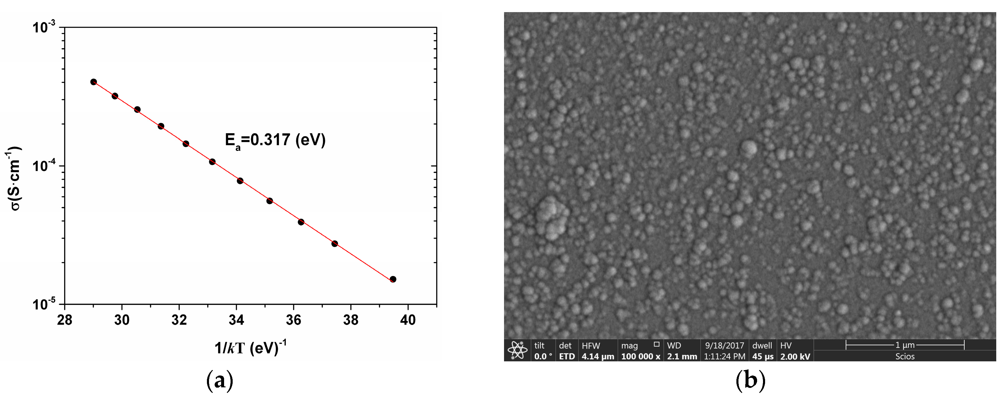
2.2. Temperature Dependence of Conductivity
2.3. Microbolometer Fabrication
2.4. Experimental Setup
3. Results
4. Conclusions
Author Contributions
Funding
Acknowledgments
Conflicts of Interest
References
- Narita, K.; Kuribayashi, R.; Altintas, E.; Someya, H.; Tsuda, K.; Ohashi, K.; Tabuchi, T.; Okubo, S.; Imazato, M.; Komatsubara, S. A plastic-based bolometer array sensor using carbon nanotubes for low-cost infrared imaging devices. Sens. Actuators A Phys. 2013, 195, 142–147. [Google Scholar] [CrossRef]
- Liger, M.; Tai, Y.-C. A 32*32 Parylene-pyrolyzed carbon bolometer imager. In Proceedings of the 19th IEEE International Conference on Micro Electro Mechanical Systems, Istanbul, Turkey, 22–26 January 2006; pp. 106–109. [Google Scholar]
- Håkansson, A.; Shahi, M.; Brill, J.W.; Fabiano, S.; Crispin, X. Conducting-polymer bolometers for low-cost IR-detection systems. Adv. Electron. Mater. 2019, 5, 1–7. [Google Scholar] [CrossRef]
- Sedky, S.; Fiorini, P.; Baert, K.; Hermans, L.; Mertens, R. Characterization and optimization of infrared poly SiGe bolometers. IEEE Trans. Electron Devices 1999, 46, 675–682. [Google Scholar] [CrossRef]
- Gray, J.; Çelik-Butler, Z.; Butler, D. MgO sacrificial layer for micromachining uncooled Y-Ba-Cu-O IR microbolometers on Si/sub 3/N/sub 4/ bridges. J. Microelectromech. Syst. 1999, 8, 192–199. [Google Scholar] [CrossRef]
- Yoneoka, S.; Liger, M.; Yama, G.; Schuster, R.; Purkl, F.; Provine, J.; Prinz, F.B.; Howe, R.T.; Kenny, T.W. ALD-metal uncooled bolometer. In Proceedings of the IEEE 24th International Conference on Micro Electro Mechanical Systems, Cancun, Mexico, 23–27 January 2011; pp. 676–679. [Google Scholar]
- Saxena, R.; Bhan, R.; Rana, P.S.; Vishwakarma, A.; Aggarwal, A.; Khurana, K.; Gupta, S. Study of performance degradation in Titanium microbolometer IR detectors due to elevated heating. Infrared Phys. Technol. 2011, 54, 343–352. [Google Scholar] [CrossRef]
- Tanaka, A.; Matsumoto, S.; Tsukamoto, N.; Itoh, S.; Chiba, K.; Endoh, T.; Nakazato, A.; Okuyama, K.; Kumazawa, Y.; Hijikawa, M.; et al. Influence of bias heating on a titanium bolometer infrared sensor. AeroSense 1997, 3061, 198–209. [Google Scholar] [CrossRef]
- Tanrikulu, M.Y.; Okyay, A.K.; Yildizak, C.; Akin, T.; Akar, O.; Sarac, A. Single layer microbolometer detector pixel using ZnO material. Infrared Technol. Appl. 2018, 10624, 1062417. [Google Scholar] [CrossRef]
- Pope, T.D.; Jerominek, H.; Alain, C.; Cayer, F.; Tremblay, B.; Grenier, C.; Topart, P.A.; LeClair, S.; Picard, F.; Larouche, C.; et al. Commercial and custom 160x120, 256x1, and 512x3 pixel bolometric FPAs. AeroSense 2002, 4721, 64–75. [Google Scholar] [CrossRef]
- Li, C.; Skidmore, G.D.; Han, C.J. Uncooled VOx infrared sensor development and application. SPIE Def. Secur. Sens. 2011, 8012, 80121. [Google Scholar] [CrossRef]
- Wang, B.; Lai, J.; Li, H.; Hu, H.; Chen, S. Nanostructured vanadium oxide thin film with high TCR at room temperature for microbolometer. Infrared Phys. Technol. 2013, 57, 8–13. [Google Scholar] [CrossRef]
- Riou, O.; Logerais, P.-O.; Durastanti, J.F. Quantitative study of the temperature dependence of normal LWIR apparent emissivity. Infrared Phys. Technol. 2013, 60, 244–250. [Google Scholar] [CrossRef]
- Han, M.-S.; Kim, D.H.; Ko, H.-J.; Shin, J.C. A fabrication and characterictics of microbolometer detectors using VOx/ZnO/VOx multilayer thin film processing. SPIE Def. Secur. 2014, 9070, 90701. [Google Scholar] [CrossRef]
- Grayli, S.V.; El-Chami, I.; Bahreyni, B.; Leach, G. Room temperature deposition of highly sensitive vanadium oxide films for infrared light sensing applications. In Proceedings of the IEEE Sensors, Busan, South Korea, 1–4 November 2015; pp. 1–4. [Google Scholar]
- Gu, D.; Zhou, X.; Guo, R.; Wang, Z.; Jiang, Y. The microstructures and electrical properties of Y-doped amorphous vanadium oxide thin films. Infrared Phys. Technol. 2017, 81, 64–68. [Google Scholar] [CrossRef]
- Ahmed, A.H.Z.; Tait, R.N.; Oogarah, T.B.; Liu, H.C.; Denhoff, M.W.; Sproule, G.; Graham, M. A surface micromachined amorphous GexSi1-xOy bolometer for thermal imaging applications. In Proceedings of the Photonic Applications in Astronomy, Biomedicine, Imaging, Materials Processing, and Education, Ottawa, ON, Canada, 26–29 September 2004; Volume 5578, pp. 298–309. [Google Scholar]
- Schimert, T.; Brady, J.; Fagan, T.; Taylor, M.; McCardel, W.; Gooch, R.; Ajmera, S.; Hanson, C.; Syllaios, A.J. Amorphous silicon based large format uncooled FPA microbolometer technology. Infrared Technol. Appl. 2008, 6940, 694023. [Google Scholar] [CrossRef]
- Ajmera, S.; Brady, J.; Hanson, C.; Schimert, T.; Syllaios, A.J.; Taylor, M. Performance improvement in amorphous silicon based uncooled microbolometers through pixel design and materials development. Infrared Technol. Appl. 2011, 8012, 80121. [Google Scholar] [CrossRef]
- Tissot, J.L.; Robert, P.; Crastes, A.; Tinnes, S.; Bercier, E.; Durand, A. Status of uncooled infrared detector technology at ULIS, France. Def. Sci. J. 2013, 63, 545–549. [Google Scholar] [CrossRef] [Green Version]
- Zhou, T.; Zuo, Y.; Qiu, K.; Zheng, J.; Wang, Q. Potential of Ti doped hydrogenated amorphous Si film with suitable resistivity and high TCR for microbolometer applications. Vacuum 2015, 119, 30–33. [Google Scholar] [CrossRef]
- Su, J.-H.; Yeh, W.-K.; Chang, W.-T.; Wu, B.-L.; Lu, J.-M.; Wang, J.-H.; Fang, Y.-K.; Chen, P.-Y. Temperature coefficient of resistance related to amorphous silicon/metal contact design of microbolometers. In Proceedings of the 3rd International Conference on Devices, Circuits and Systems (ICDCS), Coimbatore, India, 3–5 March 2016; pp. 63–67. [Google Scholar]
- Moreno, M.; Torres, A.; Calleja, C.; Lázaro, R.C.A.; Rosales, P.; Kosarev, A.; Jiménez-Zavala, R. Exploring the infrared-sensing properties of polymorphous silicon-germanium (pm-SixGey:H) thin films. Can. J. Phys. 2014, 92, 565–569. [Google Scholar] [CrossRef]
- Bronner, W.; Kleider, J.; Brüggemann, R.; Cabarrocas, P.R.I.; Mencaraglia, D.; Mehring, M. Comparison of transport and defects properties in hydrogenated polymorphous and amorphous silicon. J. Non-Cryst. Solids 2002, 299, 551–555. [Google Scholar] [CrossRef]
- Kim, K.; Johnson, E.; Abramov, A.; Cabarrocas, P.R.I. Light induced electrical and macroscopic changes in hydrogenated polymorphous silicon solar cells. EPJ Photovolt. 2012, 3, 30301. [Google Scholar] [CrossRef] [Green Version]
- Chou, Y.-P.; Lee, S.-C. Structural, optical, and electrical properties of hydrogenated amorphous silicon germanium alloys. J. Appl. Phys. 1998, 83, 4111–4123. [Google Scholar] [CrossRef]
- Jiménez-Zavala, R.; Moreno, M.; Torres, A.; Rosales, P.; Gomez, V.; Carlos, N.; Cabarrocas, P.R.I. Effect of Pressure and Flow Rates on Polymorphous Silicon-Germanium (pm-Six Ge1−x:H) Thin Films for Infrared Detection Applications. Phys. Status Solidi A 2018, 215, 1700735. [Google Scholar] [CrossRef]
- Moreno, M.; Jiménez-Zavala, R.; Torres, A.; Lázaro, R.C.A. Microbolometers based on amorphous silicon–germanium films with embedded nanocrystals. IEEE Trans. Electron Devices 2015, 62, 2120–2127. [Google Scholar] [CrossRef]
- Jiménez-Zavala, R.; Moreno, M.; Torres, A.; Rosales, P.; Sanz-Pascual, M.T.; Lázaro, R.C.A. Performance characterization of infrared detectors based on polymorphous silicon-germanium (pm-Six Ge1−x:H) thin films deposited at low temperature. Phys. Status Solidi A 2018, 215, 1700736. [Google Scholar] [CrossRef]
- Cabarrocas, P.R.I.; Chaâbane, N.; Kharchenko, A.V.; Tchakarov, S. Polymorphous silicon thin films produced in dusty plasmas: Application to solar cells. Plasma Phys. Control. Fusion 2004, 46, B235–B243. [Google Scholar] [CrossRef]
- Tanielian, M. Adsorbate effects on the electrical conductance of a-Si: H. Philos. Mag. B 1982, 45, 435–462. [Google Scholar] [CrossRef]
- Budzier, H.; Gerlach, G. Calibration of uncooled thermal infrared cameras. J. Sens. Sens. Syst. 2015, 4, 187–197. [Google Scholar] [CrossRef] [Green Version]
- Liddiard, K.C. Application of mosaic pixel microbolometer technology to very high-performance, low-cost thermography and pedestrian detection. SPIE Def. Secur. Sens. 2013, 8704, 87043. [Google Scholar] [CrossRef]
- Han, M.-S.; Kim, D.H.; Ko, H.J.; Kim, H. Vanadium oxide microbolometer using ZnO sandwich layer. Appl. Sci. Converg. Technol. 2015, 24, 178–183. [Google Scholar] [CrossRef] [Green Version]
- Ahmed, M.; Butler, D.P.; Celik-Butler, Z. Device-level vacuum packaged uncooled microbolometer on a polyimide substrate. Infrared Phys. Technol. 2016, 79, 50–57. [Google Scholar] [CrossRef] [Green Version]
- Ahmed, M.; Chitteboyina, M.M.; Butler, D.P.; Celik-Butler, Z. Temperature sensor in a flexible substrate. IEEE Sens. J. 2011, 12, 864–869. [Google Scholar] [CrossRef]
- Abdel-Rahman, M.; Al-Khalli, N.; Zia, M.F.; Alduraibi, M.; Ilahi, B.; Debbar, N.; Awad, E. Fabrication and design of vanadium oxide microbolometer. In Proceedings of the 6th International Advances in Applied Physics and Materials Science Congress & Exhibition, Istanbul, Turkey, 1–3 June 2016; Volume 1809, p. 20001. [Google Scholar]


| GeH4 (sccm) | SiH4 (sccm) | H2 (sccm) | Pressure (Torr) | Power (mW/cm2) | Temperature (°C) |
|---|---|---|---|---|---|
| 30 | 20 | 1000 | 1.2 | 90 | 200 |
| Material | pm-SixGe1-x:H This Work | VOx/ZnO [34] | a-Si:H [35,36] | VOx [37] | Poly-SiGe [4] |
|---|---|---|---|---|---|
| Size (µm2) | 50 × 50 | 50 × 50 | 35 × 35 | 25 × 25 | 50 × 50 |
| ℜv (V/W) | 2 × 10⁴ | 2 × 10⁴ | 3.7 × 10³ | 2.44 × 10⁵ | 1.64 × 10⁴ |
| NEP (W/Hz1/2) | 2 × 10⁻¹⁰ | 1 × 10⁻¹⁰ | 7.7 × 10⁻¹⁰ | 1.4 × 10⁻¹⁰ | 6 × 10⁻¹⁰ |
| D* (cm · Hz1/2/W) | 2 × 10⁷ | 4 × 10⁷ | 4.5 × 10⁶ | 1.55 × 10⁷ | 2.26 × 10⁹ |
| TCR (%/K) | 4.08 | 3.12 | 2.27 | 2.6 | 0.68 |
| R (Ω) | 15 × 103 | − | 200 × 109 | 200 × 103 | 10 × 103 |
© 2020 by the authors. Licensee MDPI, Basel, Switzerland. This article is an open access article distributed under the terms and conditions of the Creative Commons Attribution (CC BY) license (http://creativecommons.org/licenses/by/4.0/).
Share and Cite
Jimenez, R.; Moreno, M.; Torres, A.; Morales, A.; Ponce, A.; Ferrusca, D.; Rangel-Magdaleno, J.; Castro-Ramos, J.; Hernandez-Perez, J.; Cano, E. Fabrication of Microbolometer Arrays Based on Polymorphous Silicon–Germanium. Sensors 2020, 20, 2716. https://doi.org/10.3390/s20092716
Jimenez R, Moreno M, Torres A, Morales A, Ponce A, Ferrusca D, Rangel-Magdaleno J, Castro-Ramos J, Hernandez-Perez J, Cano E. Fabrication of Microbolometer Arrays Based on Polymorphous Silicon–Germanium. Sensors. 2020; 20(9):2716. https://doi.org/10.3390/s20092716
Chicago/Turabian StyleJimenez, Ricardo, Mario Moreno, Alfonso Torres, Alfredo Morales, Arturo Ponce, Daniel Ferrusca, Jose Rangel-Magdaleno, Jorge Castro-Ramos, Julio Hernandez-Perez, and Eduardo Cano. 2020. "Fabrication of Microbolometer Arrays Based on Polymorphous Silicon–Germanium" Sensors 20, no. 9: 2716. https://doi.org/10.3390/s20092716
APA StyleJimenez, R., Moreno, M., Torres, A., Morales, A., Ponce, A., Ferrusca, D., Rangel-Magdaleno, J., Castro-Ramos, J., Hernandez-Perez, J., & Cano, E. (2020). Fabrication of Microbolometer Arrays Based on Polymorphous Silicon–Germanium. Sensors, 20(9), 2716. https://doi.org/10.3390/s20092716