
A Novel Analytical Design Technique for a Wideband Wilkinson Power Divider Using Dual-Band Topology

 ,
,  , ,
, , 
Abstract
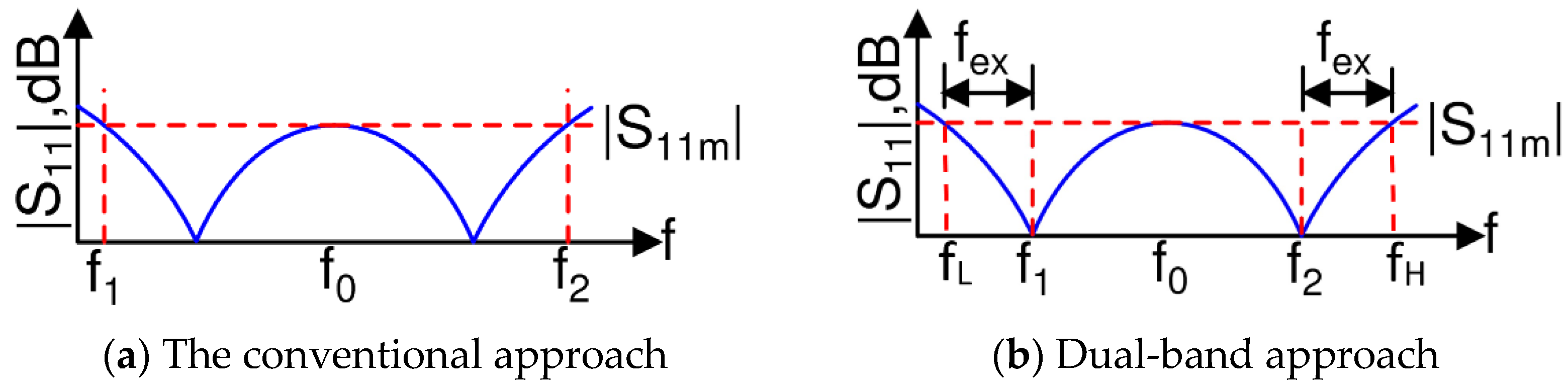
:1. Introduction
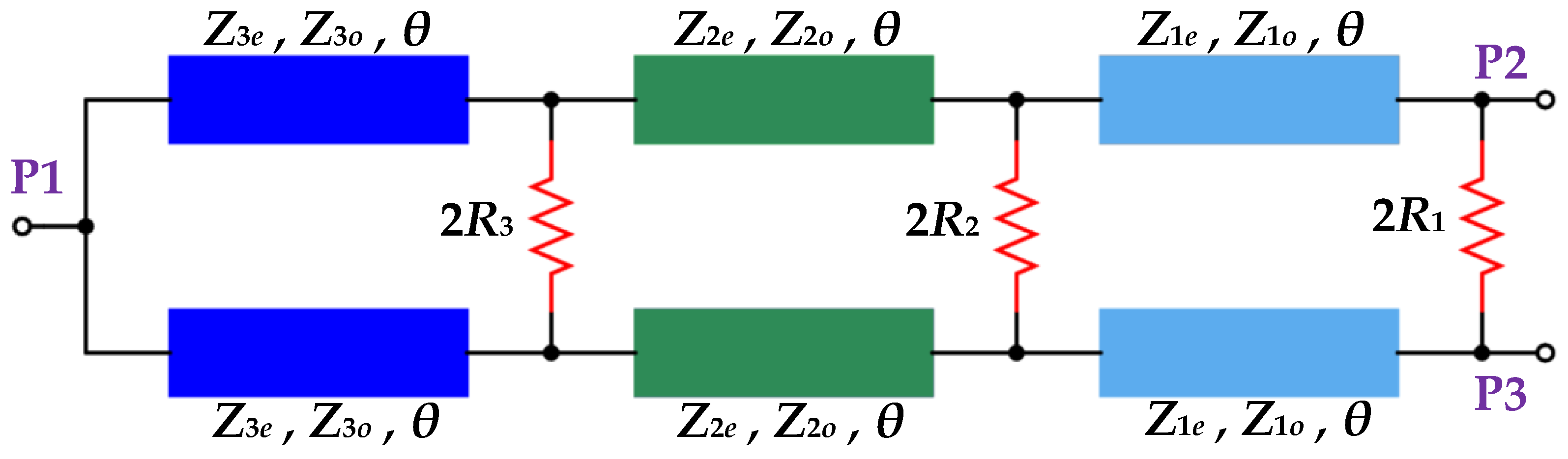
2. The Proposed Analytical Design Equations of the WPD
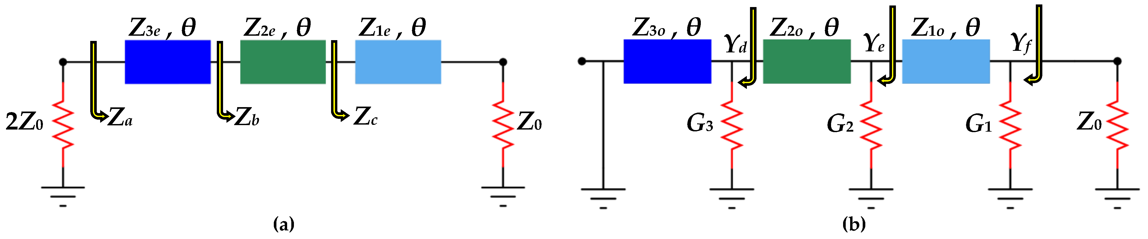
2.1. Even-Mode Analysis
2.2. Odd-Mode Analysis
3. The Scattering Parameters of the WPD and BW Determination
3.1. Expressions of Even-Mode S-Parameters
3.2. Expression of Odd-Mode S-Parameters
3.3. Maximum Input Return loss (RL) between f1 and f2
Some Special Cases for Input RL
- (i)
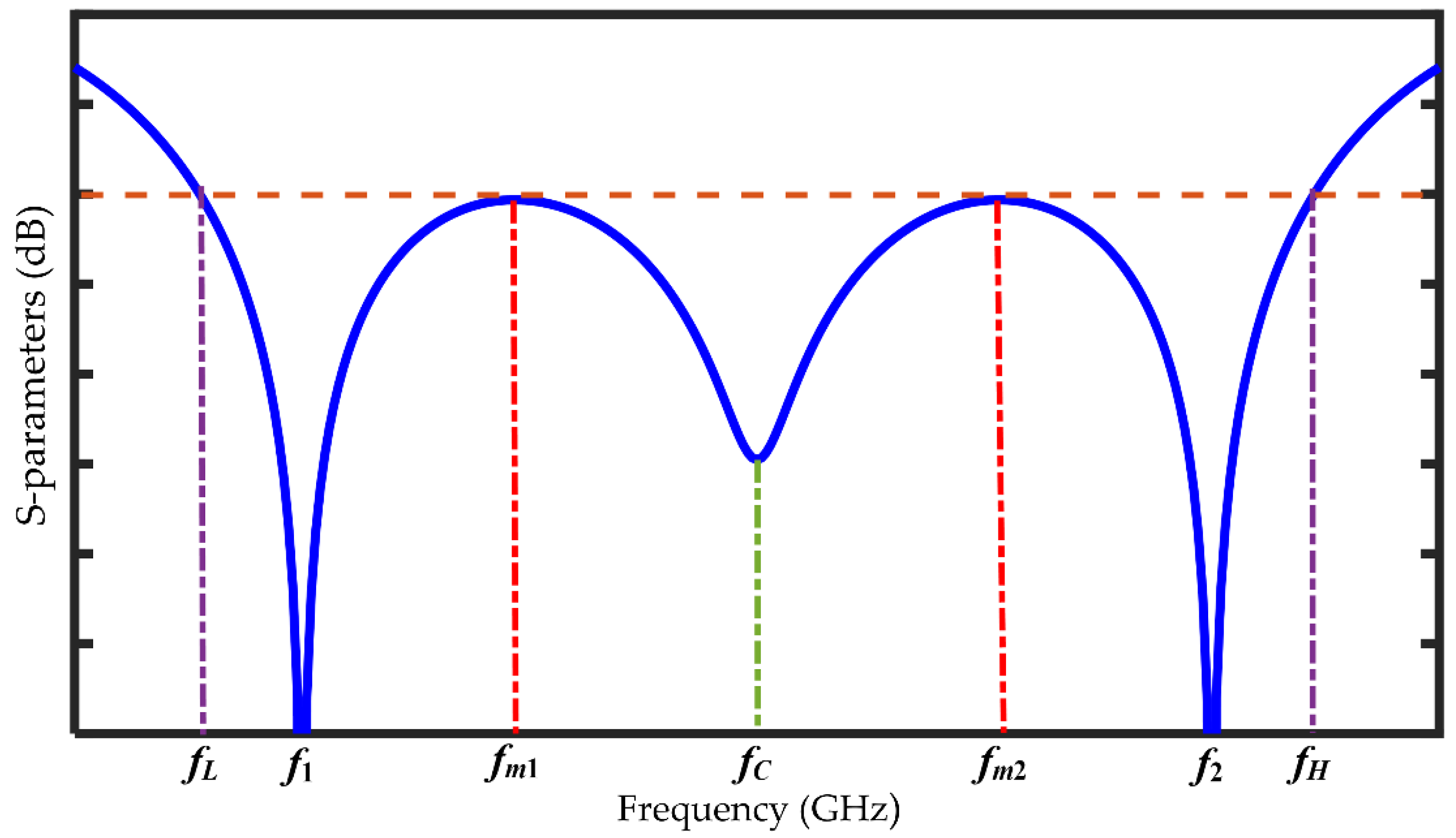
- Using (55) and (63), the common realizable solutions of a, irrespective of the value of r, can be found as:These values of a correspond to the values of |S11|dB at f1 and f2 where we will always get two minima, which is also evident from (6) owing to the dual-band principle. Now applying any suitable numerical analysis tool, we can calculate two other real values of a (am1 and am2). These values of a indicate two maxima of |S11|dB at fm1 and fm2 where f1 < fm1 < fc and fc < fm2 < f2 and the center frequency, fc = 0.5(f1 + f2) = 0.5(fL + fH). These frequency levels are graphically defined in Figure 4.Furthermore, since θ ∝ f, the following equations can be derived with the help of (2) for which |S11|dB becomes the maximum.Some examples are shown in Table 1 where different solutions of a from (63) have been tabulated.
- (ii)
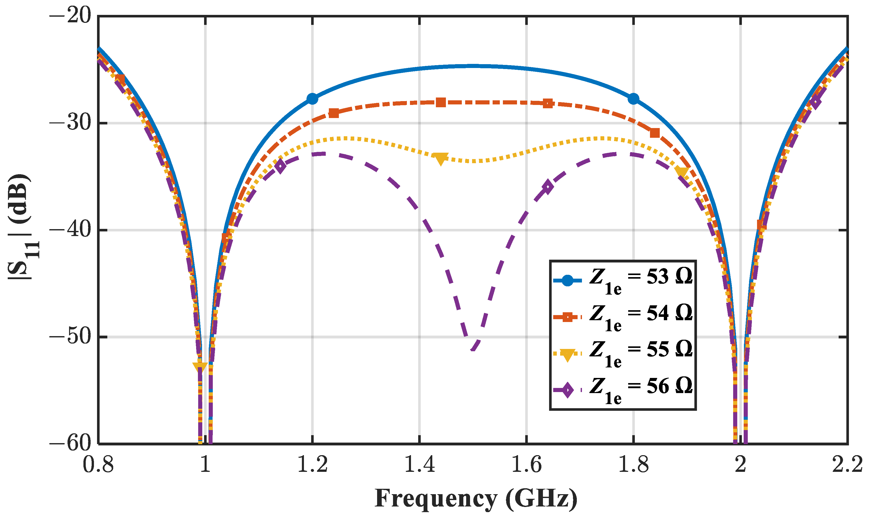
- From (62), it can be further deduced that, for the minimum band-limited region (f1 < f < f2), we have the following cases.For this case, we can obtain two minima at f1, f2, and one maximum at fc. Thus, the achievable BW can be found at the |S11(fc)|dB level which is also visible from Figure 5 (Z1e = 53 Ω and 54 Ω as examples where |S11(fc)| = −25 dB and −28 dB, respectively).For this case, we can obtain two minima at f1, f2, and two equal maxima at fm1, fm2. Thus, the achievable BW can be found at the |S11(fm1)|dB level which is also visible from Figure 5 (Z1e = 55 Ω as an example where |S11(f m1)| = −31.5 dB).For the above case, we will get the minimum possible value at fc, and this can be visualized from Figure 5 (Z1e = 56 Ω as an example). Also in this case, we will get three minima at f1, fc and f2, and two equal maxima at fm1 and fm2. This is also the point beyond which the maxima of S11 cannot be lowered further by choosing any value of Z1e, Z2e, or Z3e. So, it will give the best possible BW with the lowest possible |S11|dB and the achievable BW can be found at the |S11(fm1)|dB level where |S11(f m1)| = −33 dB as seen for Z1e = 56 Ω.Hence, from the value of k3/k6, we can decide which design parameters to choose to arrive at either of the above three cases. In a special case when k3 = 0, it can be inferred from (55) thatConsequently, choosing Z2e = Z0 as a particular solution of (18) and using (75), we conclude the following.Thus, after finding Z1e that ensures S11 = 0, Equation (76) can be used to find Z3e which gives the best possible maxima of S11 between f1 and f2. This equation will not be applicable unless the best possible maxima of S11 is targeted.
- (iii)
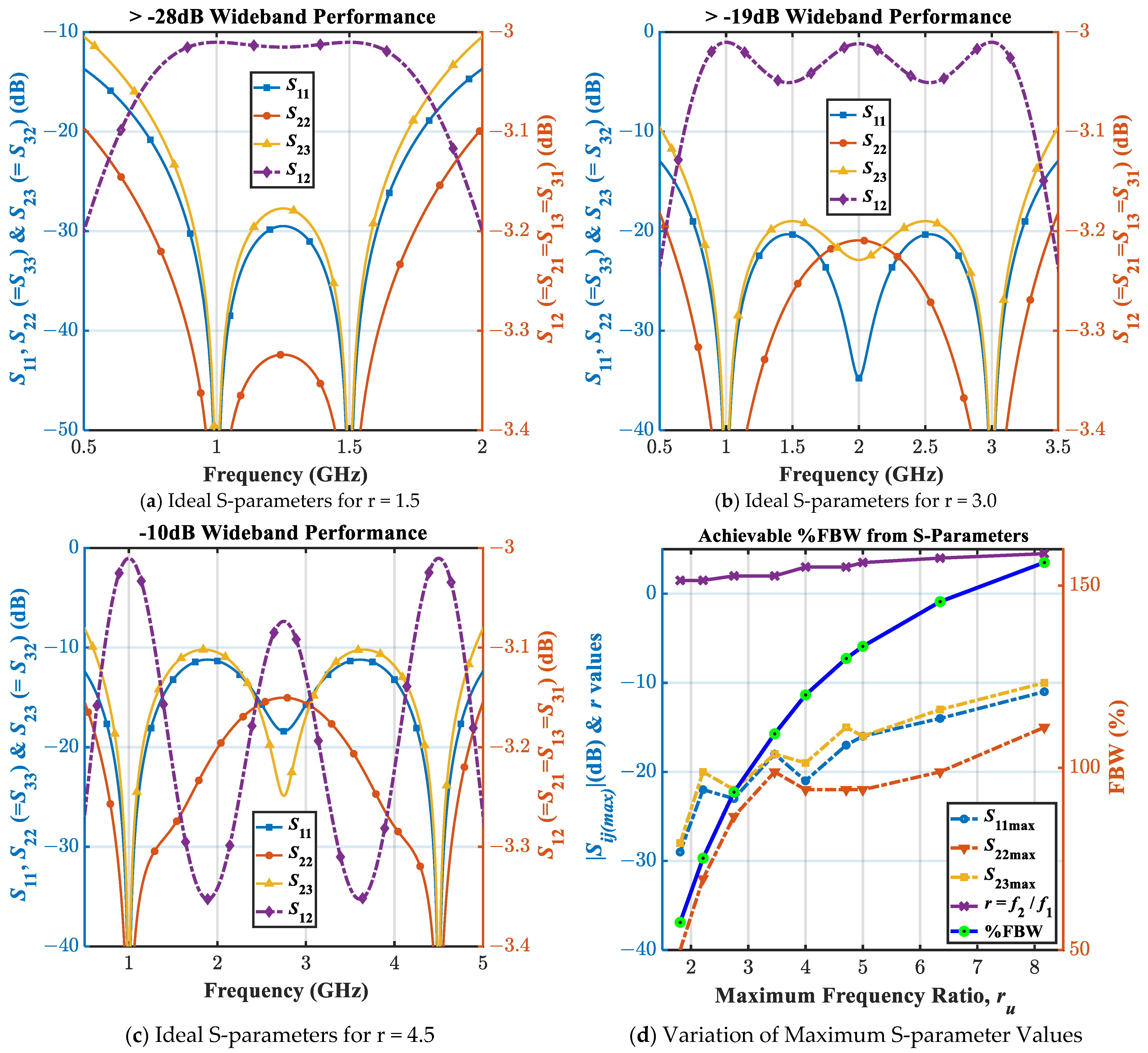
- Based on the variation of maxima of S11 versus Z1e shown in Figure 6, it is apparent that the higher bandwidth level can be achieved from the lower values of r. In fact, for r = 5, it is not possible to achieve 10 dB return loss as depicted in Figure 6. Further, the best possible maxima can be achieved for a certain value of Z1e. From that value of Z1e shown in Figure 6, we can calculate Z2e and Z3e from (18) and (12) respectively. It can be verified that these values of Z1e, Z2e, and Z3e also satisfy (76).
3.4. Maximum Output Return Loss (RL) and Isolation between f1 and f2
4. The Proposed Design Methodology
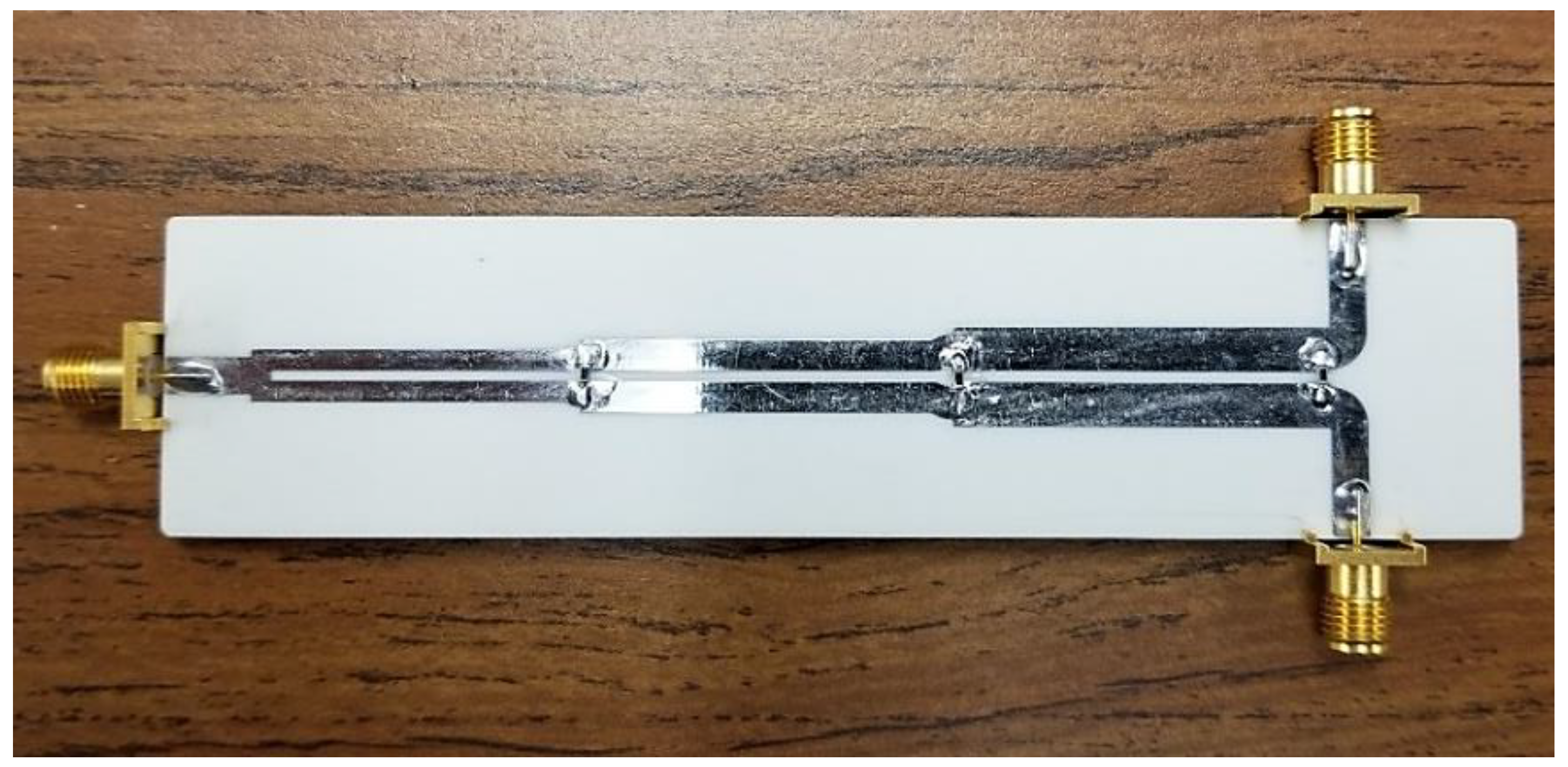
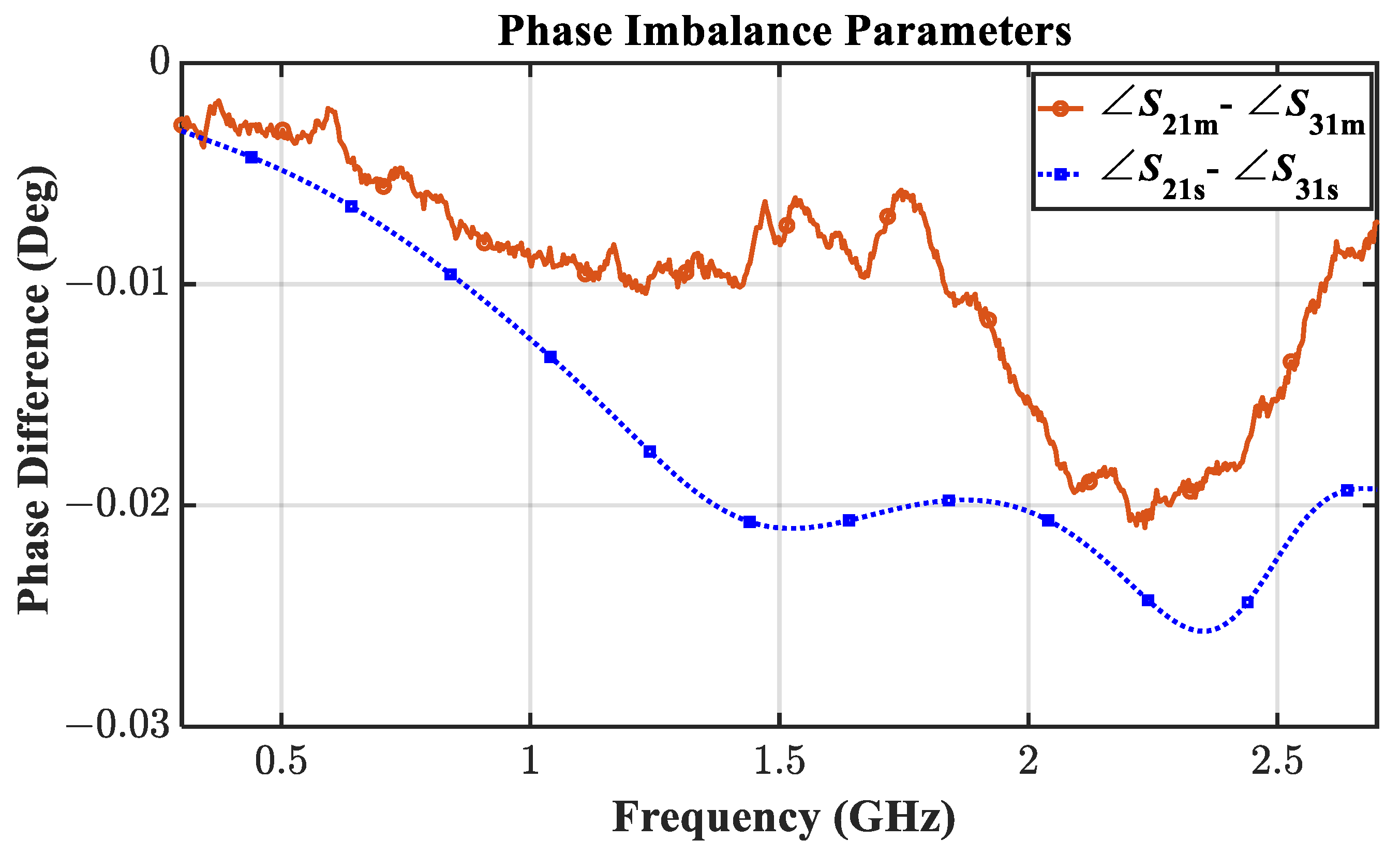
5. The Fabricated Prototype and Measurement Results
6. Conclusions
Author Contributions
Funding
Institutional Review Board Statement
Informed Consent Statement
Data Availability Statement
Acknowledgments
Conflicts of Interest
References
- Pozar, D.M. Microwave Engineering, 4th ed.; John Wiley & Sons, Inc.: Hoboken, NJ, USA, 2012. [Google Scholar]
- Wilkinson, E.J. An N-way hybrid power divider. IEEE Trans. Microw. Theory Tech. 1960, 8, 116–118. [Google Scholar] [CrossRef]
- Cohn, S.B. A class of broadband three-port TEM-mode hybrids. IEEE Trans. Microw. Theory Tech. 1968, 16, 110–116. [Google Scholar] [CrossRef] [Green Version]
- Oraizi, H.; Sharifi, A.-R. Design and optimization of broadband asymmetrical multisection wilkinson power divider. IEEE Trans. Microw. Theory Tech. 2006, 54, 2220–2231. [Google Scholar] [CrossRef]
- Honari, M.; Mirzavand, L.; Mirzavand, R.; Abdipour, A.; Mousavi, P. Theoretical design of broadband multisection Wilkinson power dividers with arbitrary power split ratio. IEEE Trans. Compon. Packag. Manuf. Technol. 2016, 6, 605–612. [Google Scholar] [CrossRef]
- Ehsan, N.; Vanhille, K.; Rondineau, S.; Cullens, E.D.; Popović, Z.B. Broadband micro-coaxial Wilkinson dividers. IEEE Trans. Microw. Theory Tech. 2009, 57, 2783–2789. [Google Scholar] [CrossRef]
- Lim, J.-S.; Park, U.-H.; Oh, S.; Koo, J.-J.; Jeong, Y.-C.; Ahn, D. A 800- to 3200-MHz wideband CPW balun using multistage Wilkinson structure. In Proceedings of the 2006 IEEE MTT-S International Microwave Symposium Digest, San Francisco, CA, USA, 11–16 June 2006; pp. 1141–1144. [Google Scholar]
- Wentzel, A.; Subramanian, V.; Sayed, A.; Boeck, G. Novel broadband Wilkinson power combiner. In Proceedings of the 2006 European Microwave Conference, Manchester, UK, 10–15 September 2006; pp. 212–215. [Google Scholar]
- Chiu, L.; Yum, T.Y.; Xue, X.; Chan, C.H. A wideband compact parallel-strip 180 Wilkinson power divider for push–pull circuitries. IEEE Microw. Wireless Compon. Lett. 2006, 16, 49–51. [Google Scholar] [CrossRef]
- Wong, S.W.; Zhu, L. Ultra-wideband power dividers with good isolation and sharp roll-off skirt. IEEE Microw. Wireless Compon. Lett. 2008, 18, 518–520. [Google Scholar] [CrossRef]
- Lan, X.; Chang-Chien, P.; Fong, F.; Eaves, D.; Zeng, X.; Kintis, M. Ultra-wideband power divider using multi-wafer packaging technology. IEEE Microw. Wireless Compon. Lett. 2011, 21, 46–48. [Google Scholar] [CrossRef]
- Sun, Y.; Freundorfer, A.P. Broadband folded Wilkinson power splitter. IEEE Microw. Wireless Compon. Lett. 2004, 14, 295–297. [Google Scholar] [CrossRef]
- Chen, C.-C.; Cin, J.-J.; Wang, S.-H.; Lin, C.-C.; Tzuang, C.-K.C. A novel miniaturized wideband Wilkinson power divider employing two-dimensional transmission line. In Proceedings of the 2008 IEEE International Symposium on VLSI Design, Automation and Test (VLSI-DAT), Hsinchu, Taiwan, 23–25 April 2008; pp. 212–215. [Google Scholar]
- Chiang, M.-J.; Wu, H.-S.; Tzuang, C.-K.C. A -band CMOS Wilkinson power divider using synthetic quasi-TEM transmission lines. IEEE Microw. Wireless Compon. Lett. 2007, 17, 837–839. [Google Scholar] [CrossRef]
- Park, M.-J. Dual-band Wilkinson divider with coupled output port extensions. IEEE Trans. Microw. Theory Tech. 2009, 57, 2232–2237. [Google Scholar] [CrossRef]
- Wu, Y.; Liu, Y.; Xue, Q. An analytical approach for a novel coupled-line dual-band Wilkinson power divider. IEEE Trans. Microw. Theory Tech. 2011, 59, 286–294. [Google Scholar] [CrossRef]
- Chang, T.-J.; Tsao, Y.-F.; Huang, T.-J.; Hsu, H.-T. Bandwidth Improvement of Conventional Dual-Band Power Divider Using Physical Port Separation Structure. Electronics 2020, 9, 2192. [Google Scholar] [CrossRef]
- Vincenti Gatti, R.; Rossi, R.; Dionigi, M. Wideband Rectangular Waveguide to Substrate Integrated Waveguide (SIW) E-Plane T-Junction. Electronics 2021, 10, 264. [Google Scholar] [CrossRef]
- Kawai, T.; Yamasaki, J.; Kokubo, Y.; Ohta, I. A design method of dual-frequency Wilkinson power divider. In Proceedings of the 2006 Asia-Pacific Microwave Conference, Yokohama, Japan, 12–15 December 2006; pp. 913–916. [Google Scholar]
- Wang, X.; Sakagami, I. Generalized dual-frequency Wilkinson power dividers with a series/parallel RLC circuit. In Proceedings of the 2011 IEEE MTT-S International Microwave Symposium, Baltimore, MD, USA, 5–10 June 2011; pp. 1–4. [Google Scholar]
- Wu, Y.; Liu, Y.; Li, S. Unequal dual-frequency Wilkinson power divider including series resistor-inductor-capacitor isolation structure. IET Microw. Antennas Propag. 2009, 3, 1079–1085. [Google Scholar] [CrossRef]
- Wu, Y.; Liu, Y.; Zhang, Y.; Gao, J.; Zhou, H. A dual band unequal Wilkinson power divider without reactive components. IEEE Trans. Microw. Theory Tech. 2009, 57, 216–222. [Google Scholar]
- Genc, A.; Baktur, R. Dual-and triple-band Wilkinson power dividers based on composite right-and left-handed transmission lines. IEEE Trans. Compon. Packag. Manuf. Tech. 2011, 1, 327–334. [Google Scholar] [CrossRef]
- Kao, J.-C.; Tsai, Z.-M.; Lin, K.-Y.; Wang, H. A modified Wilkinson power divider with isolation bandwidth improvement. IEEE Trans. Microw. Theory Tech. 2012, 60, 2768–2780. [Google Scholar] [CrossRef]
- Wang, Y.; Zhang, Y.X.; Liu, X.F.; Lee, C.J. A compact bandpass Wilkinson power divider with ultra-wide band harmonic suppression. IEEE Microw. Wirel. Compon. Lett. 2017, 27, 888–890. [Google Scholar] [CrossRef]
- Chen, M.T.; Tang, C.W. Design of the filtering power divider with a wide passband and stopband. IEEE Microw. Wirel. Compon. Lett. 2018, 28, 570–572. [Google Scholar] [CrossRef]
- Tas, V.; Atalar, A. An optimized isolation network for the Wilkinson divider. IEEE Trans. Microw. Theory Tech. 2014, 62, 3393–3402. [Google Scholar] [CrossRef] [Green Version]
- Cheng, P.; Wang, Q.; Li, W.; Jia, Y.; Liu, Z.; Feng, C.; Jiang, L.; Xiao, H.; Wang, X. A Broadband Asymmetrical GaN MMIC Doherty Power Amplifier with Compact Size for 5G Communications. Electronics 2021, 10, 311. [Google Scholar] [CrossRef]
- Nouri, M.E.; Roshani, S.; Mozaffari, M.H.; Nosratpour, A. Design of high-efficiency compact Doherty power amplifier with harmonics suppression and wide operation frequency band. AEU Int. J. Electron. C. 2020, 118, 153168. [Google Scholar] [CrossRef]
- Hookari, M.; Roshani, S.; Roshani, S. High-efficiency balanced power amplifier using miniaturized harmonics suppressed coupler. Int. J. RF Microw. Comput. -Aided Eng. 2020, 30, e22252. [Google Scholar] [CrossRef]
- Tseng, C.H.; Chang, C.L. Improvement of return loss bandwidth of balanced amplifier using metamaterial-based quadrature power splitters. IEEE Microw. Wireless Compon. Lett. 2008, 18, 269–271. [Google Scholar] [CrossRef]
- Islam, R.; Maktoomi, M.H.; Gu, Y.; Arigong, B. Concurrent Dual-Band Microstrip Line Hilbert Transformer for Spectrum Aggregation Real-Time Analog Signal Processing. In Proceedings of the 2020 IEEE/MTT-S International Microwave Symposium (IMS), Los Angeles, CA, USA, 4–6 August 2020; pp. 900–903. [Google Scholar]
- Islam, R.; Maktoomi, M.H.; Ren, H.; Arigong, B. Spectrum Aggregation Dual-Band RealTime RF/Microwave Analog Signal Processing from Microstrip Line High-Frequency Hilbert Transformer. IEEE Trans. Microw. Theory Tech. 2021, 1, 1. [Google Scholar] [CrossRef]
- Boutayeb, H.; Watson, P.R.; Lu, W.; Wu, T. Beam switching dual polarized antenna array with reconfigurable radial waveguide power dividers. IEEE Trans. Antenn Propag. 2016, 65, 1807–1814. [Google Scholar] [CrossRef]
- Gao, S.S.; Sun, S.; Xiao, S. A novel wideband bandpass power divider with harmonic-suppressed ring resonator. IEEE Microw. Wireless Compon. Lett. 2013, 23, 119–121. [Google Scholar] [CrossRef] [Green Version]
- Zhang, B.; Yu, C.; Liu, Y. Compact power divider with bandpass response and improved out-of-band rejection. J. Electromagn. Waves Appl. 2016, 30, 1124–1132. [Google Scholar] [CrossRef]
- Maktoomi, M.A.; Akbarpour, M.; Hashmi, M.S.; Ghannouchi, F.M. On the dual frequency impedance/admittance characteristic of multi-section commensurate transmission-line. IEEE Trans. on Circuits Syst. II Exp. Briefs 2017, 64, 665–669. [Google Scholar] [CrossRef]
- Kim, S.-H.; Yoon, J.-H.; Kim, Y.; Yoon, Y.-C. A modified Wilkinson divider using zero-degree phase shifting composite right/left-handed transmission line. In Proceedings of the 2010 IEEE MTT-S International Microwave Symposium, Anaheim, CA, USA, 23–28 May 2010; pp. 1556–1559. [Google Scholar]
- Trantanella, C.J. A novel power divider with enhanced physical and electrical port isolation. In Proceedings of the 2010 IEEE MTT-S International Microwave Symposium, Anaheim, CA, USA, 23–28 May 2010; pp. 129–132. [Google Scholar]
- Song, K.; Xue, Q. Novel ultra-wideband (UWB) multilayer slotline power divider with bandpass response. IEEE Microw. Wireless Compon. Lett. 2010, 20, 13–15. [Google Scholar] [CrossRef]
- Liu, Y.; Sun, S.; Yu, X.; Wu, Y.; Liu, Y. Design of a wideband filtering power divider with good in-band and out-of-band isolations. Int. J. RF Microw. Comput. Aid Eng. 2019, 29, e21728. [Google Scholar] [CrossRef]
- Okada, Y.; Kawai, T.; Enokihara, A. Wideband lumped-element Wilkinson power dividers using LC-ladder circuits. In Proceedings of the 2015 European Microwave Conference (EuMC), Paris, France, 7–10 September 2015; pp. 115–118. [Google Scholar]
- Maktoomi, M.A.; Hashmi, M.S.; Ghannouchi, F.M. Theory and design of a novel wideband DC isolated Wilkinson power divider. IEEE Microw. Wireless Compon. Lett. 2016, 26, 586–588. [Google Scholar] [CrossRef]
- Tang, C.-W.; Chen, J.-T. A design of 3-dB wideband microstrip power divider with an ultra-wide isolated frequency band. IEEE Trans. Microw. Theory Tech. 2016, 64, 1806–1811. [Google Scholar] [CrossRef]
- Jiao, L.; Wu, Y.; Liu, Y.; Xue, Q.; Ghassemlooy, Z. Wideband filtering power divider with embedded transversal signal-interference sections. IEEE Microw. Wireless Compon. Lett. 2017, 27, 1068–1070. [Google Scholar] [CrossRef]
- Wang, X.; Ma, Z.; Xie, T.; Ohira, M.; Chen, C.-P.; Lu, G. Synthesis Theory of Ultra-Wideband Bandpass Transformer and its Wilkinson Power Divider Application with Perfect in-Band Reflection/Isolation. IEEE Trans. Microw. Theory Tech. 2019, 67, 3377–3390. [Google Scholar] [CrossRef]
- Liu, Y.; Zhu, L.; Sun, S. Proposal and Design of a Power Divider with Wideband Power Division and Port-to-Port Isolation: A New Topology. IEEE Trans. Microw. Theory Tech. 2020, 68, 1431–1438. [Google Scholar] [CrossRef]
- Bao, C.; Wang, X.; Ma, Z.; Chen, C.-P.; Lu, G. An Optimization Algorithm in Ultrawideband Bandpass Wilkinson Power Divider for Controllable Equal-Ripple Level. IEEE Microw. Wireless Compon. Lett. 2020, 30, 861–864. [Google Scholar] [CrossRef]


| Band Ratio, r | Zke Values, k ϵ {1, 2, 3} | Solution of a | Remarks on |S11|dB from the Value of a | ||
|---|---|---|---|---|---|
| Z1e (Ω) | Z2e (Ω) | Z3e (Ω) | |||
| 2 | 56.1520 | 70.7107 | 89.0442 | Minima at f1 & f2 | |
| Maxima at fm1 & fm2 | |||||
| 3 | 59.5380 | 70.7107 | 83.9807 | Minima at f1 & f2 | |
| Maxima at fm1 & fm2 | |||||
| 4 | 64.3670 | 70.7106 | 77.6800 | Minima at f1 & f2 | |
| Maxima at fm1 & fm2 | |||||
| r | Z1e (Ω) | Z1o (Ω) | Z2e (Ω) | Z2o (Ω) | Z3e (Ω) | Z3o (Ω) | R1 (Ω) | R2 (Ω) | R3 (Ω) |
|---|---|---|---|---|---|---|---|---|---|
| 1.5 | 60.00 | 37.00 | 81.26 | 42.00 | 99.04 | 50.00 | 929.00 | 31.26 | 5.01 |
| 2 | 58.30 | 34.80 | 73.38 | 40.00 | 92.45 | 48.00 | 500.00 | 34.52 | 5.00 |
| 3 | 59.00 | 36.00 | 70.72 | 37.00 | 83.22 | 41.00 | 910.00 | 84.20 | 23.45 |
| 3.5 | 60.00 | 36.00 | 71.45 | 38.00 | 78.64 | 44.00 | 1000.00 | 81.60 | 31.15 |
| 4 | 63.00 | 35.00 | 71.66 | 42.00 | 76.04 | 43.00 | 355.00 | 76.25 | 37.42 |
| 4.5 | 64.50 | 34.00 | 73.26 | 40.00 | 71.17 | 41.00 | 151.00 | 109.49 | 39.42 |
| Minimum Band Ratio, R | Minimum of Return loss & Isolation (dB) | Maximum Insertion loss (dB) | Operating Band Range, fL to fH (GHz) | Extra BW, fex (GHz) | Attainable Band Ratio, ru |
|---|---|---|---|---|---|
| 1.50 | 28 | 3.01 | 0.89–1.61 | 0.11 | 1.81 |
| 10 | 3.20 | 0.48–2.02 | 0.52 | 4.21 | |
| 2.00 | 20 | 3.02 | 0.80–2.20 | 0.20 | 2.75 |
| 10 | 3.20 | 0.50–2.50 | 0.50 | 5.00 | |
| 3.00 | 19 | 3.05 | 0.80–3.20 | 0.20 | 4.00 |
| 10 | 3.21 | 0.52–3.48 | 0.48 | 6.69 | |
| 3.50 | 16 | 3.11 | 0.75–3.75 | 0.25 | 6.35 |
| 10 | 3.22 | 0.55–3.95 | 0.45 | 7.77 | |
| 4.00 | 13 | 3.20 | 0.68–4.32 | 0.32 | 5.00 |
| 10 | 3.22 | 0.57–4.43 | 0.43 | 7.18 | |
| 4.50 | 10 | 3.35 | 0.60–4.90 | 0.40 | 8.17 |
| 3rd Line (n = 3) | 2nd Line (n = 2) | 1st Line (n = 1) | |
|---|---|---|---|
| Wn (in mm) | 1.918 | 2.823 | 3.987 |
| Sn (in mm) | 0.854 | 0.919 | 0.999 |
| Ln (in mm) | 29.66 | 33.62 | 33.82 |
| Reference | Techniques/Topology | Band Ratio (ru = fH/fL) | Min. Input RL (dB) | Min. Output RL (dB) | Min. Isolation level (dB) | Max. Insertion level (dB) | Max. Phase Imbalance of Outport Ports (Degree) | FBW (%) |
|---|---|---|---|---|---|---|---|---|
| [24] | RLCT Isolation network | 3.55 | 10 | 10 | 20 | 4.00 | - | 112.00 |
| [25] | Frequency-selecting coupling structure | 2.13 | 20 | - | 12 | 3.40 | 4.00 | 62.07 |
| [26] | Parallel coupled filters | 1.66 | 15 | 14 | 22 | 4.00 | - | 49.50 |
| [27] | Single section optimized isolation network | 2.20 | 19 | 20 | 19 | 3.20 | - | 75.00 |
| [35] | Two open-circuited stubs and three coupled lines | 1.90 | 10 | 10 | 10 | - | 2.50 | 62.00 |
| [39] | Isolation stage shifting | 2.08 | - | - | 17 | 3.90 | - | 70.20 |
| [40] | Multilayer slot line structure | 3.22 | 10 | 10 | 10 | 5.00 | 2.00 | 105.30 |
| [41] | Hybrid Wilkinson and Gysel structure | 1.78 | 16 | 17 | 20 | 4.40 | 1.70 | 56.00 |
| [42] | LC ladder | 3.08 | 18 | 17 | 18 | 3.90 | - | 102.00 |
| [43] | Port matching using three coupled-line, one T-line and one isolation resistor | 2.00 | 15 | 17 | 15 | 3.20 | 0.50 | 66.67 |
| [44] | Quasi-coupled line with one open stub and two shorted stubs | 3.19 | 15 | 15 | 15 | 3.66 | 6.80 | 104.50 |
| [45] | Transversal filters with RLC network | 2.57 | 15 | 15 | 17 | - | 1.60 | 87.80 |
| [46] | Four T-lines, two stubs & five resistors | 3.42 | 17.8 | 20 | 19.8 | 4.00 | - | 109.50 |
| [47] | Port-to-Port isolation structure | 2.28 | 10 | 10 | 17.5 | 3.70 | 1.50 | 78.00 |
| [48] | Synthesis theory and optimization algorithm | 1.92 | 21.1 | 19.2 | 18.5 | 3.10 | 1.20 | 63.00 |
| This Work | Three Coupled T-Lines & three isolation resistors | 3.45 | 16.4 | 15 | 22 | 3.30 | 0.017 | 110.11 |
| 5.78 | 15.9 | 12 | 10 | 3.50 | 0.021 | 141.00 |
Publisher’s Note: MDPI stays neutral with regard to jurisdictional claims in published maps and institutional affiliations. |
© 2021 by the authors. Licensee MDPI, Basel, Switzerland. This article is an open access article distributed under the terms and conditions of the Creative Commons Attribution (CC BY) license (https://creativecommons.org/licenses/by/4.0/).
Share and Cite
Omi, A.I.; Islam, R.; Maktoomi, M.A.; Zakzewski, C.; Sekhar, P. A Novel Analytical Design Technique for a Wideband Wilkinson Power Divider Using Dual-Band Topology. Sensors 2021, 21, 6330. https://doi.org/10.3390/s21196330
Omi AI, Islam R, Maktoomi MA, Zakzewski C, Sekhar P. A Novel Analytical Design Technique for a Wideband Wilkinson Power Divider Using Dual-Band Topology. Sensors. 2021; 21(19):6330. https://doi.org/10.3390/s21196330
Chicago/Turabian StyleOmi, Asif I., Rakibul Islam, Mohammad A. Maktoomi, Christine Zakzewski, and Praveen Sekhar. 2021. "A Novel Analytical Design Technique for a Wideband Wilkinson Power Divider Using Dual-Band Topology" Sensors 21, no. 19: 6330. https://doi.org/10.3390/s21196330
APA StyleOmi, A. I., Islam, R., Maktoomi, M. A., Zakzewski, C., & Sekhar, P. (2021). A Novel Analytical Design Technique for a Wideband Wilkinson Power Divider Using Dual-Band Topology. Sensors, 21(19), 6330. https://doi.org/10.3390/s21196330