
A CMOS PSR Enhancer with 87.3 mV PVT-Insensitive Dropout Voltage for Sensor Circuits


Abstract
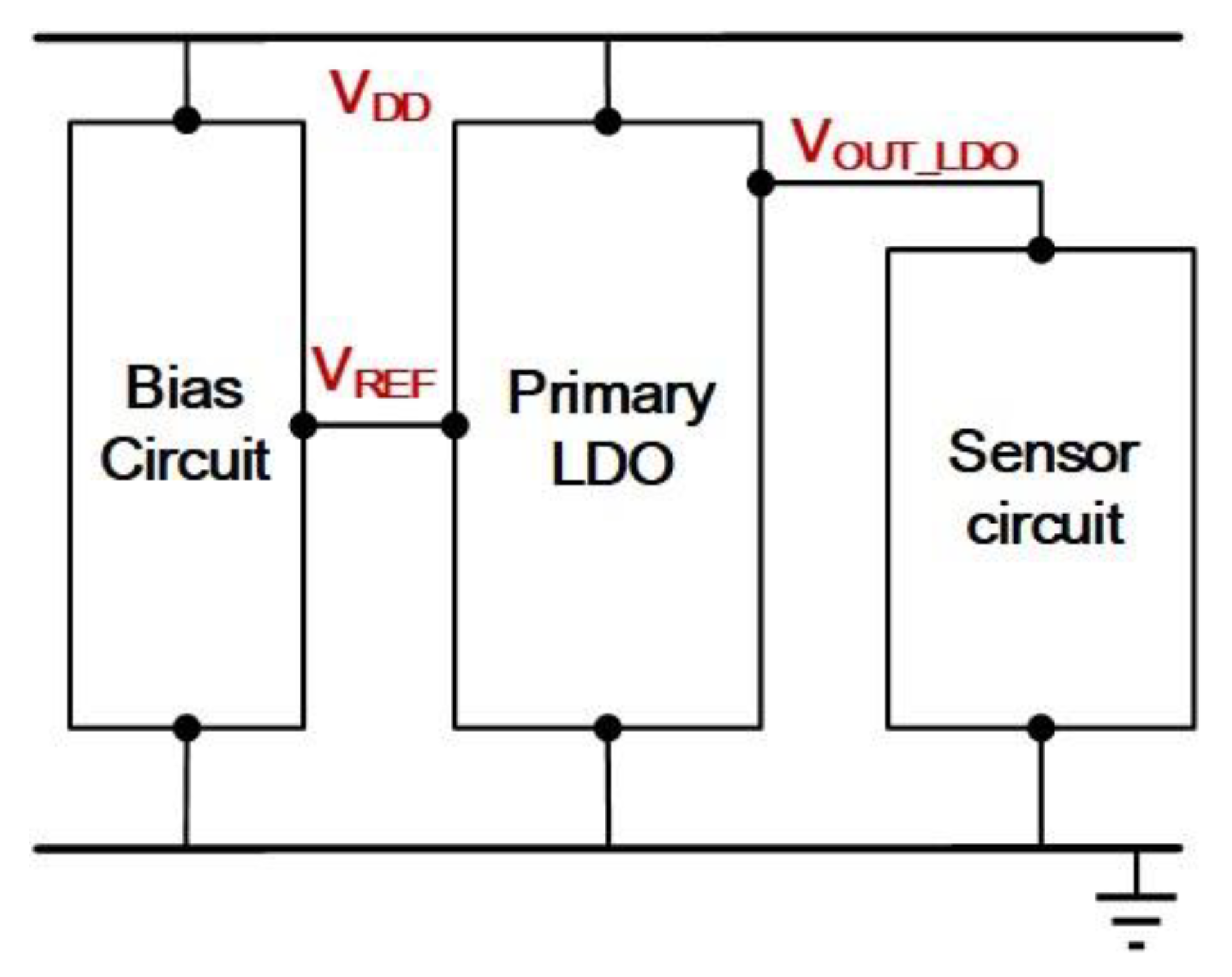
:1. Introduction
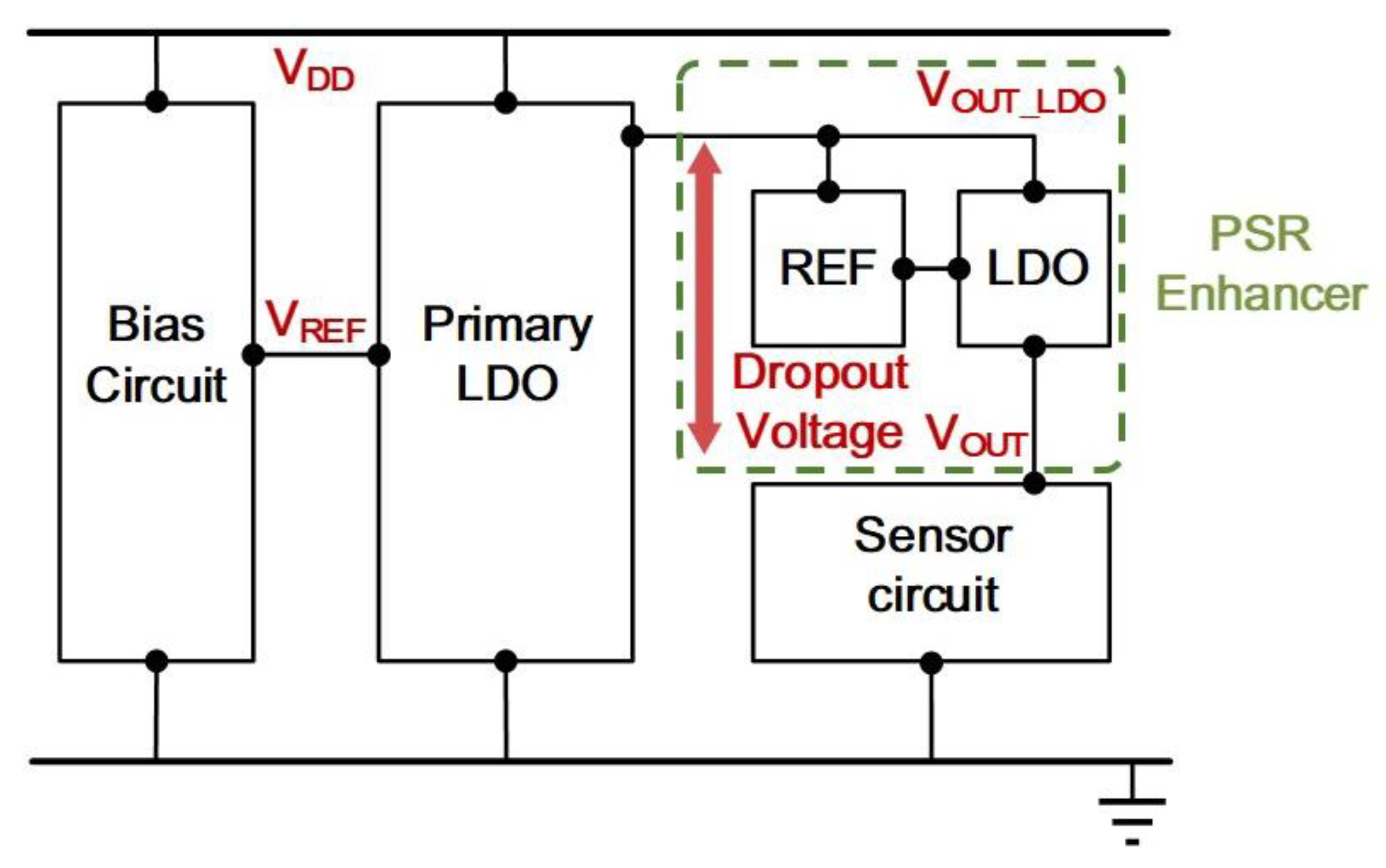
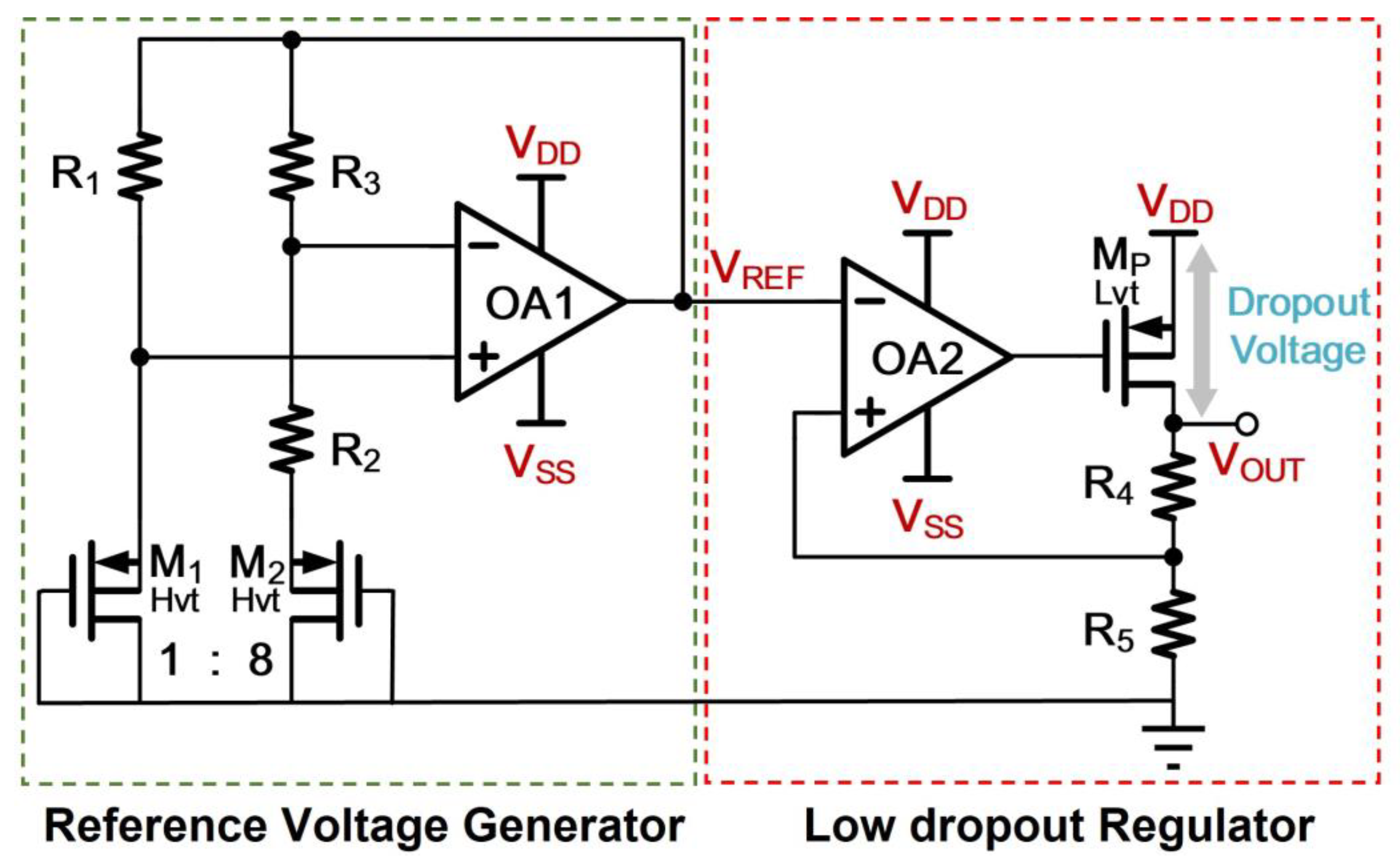
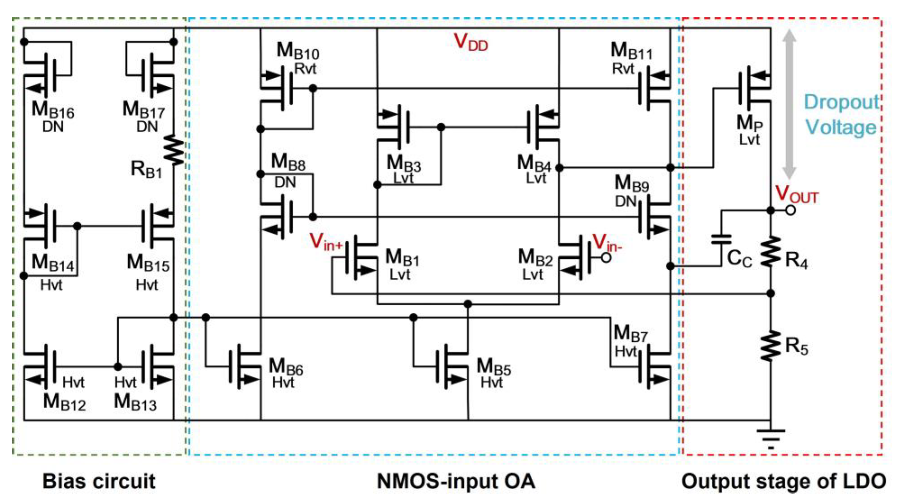
2. Conventional PSR Enhancer Circuit and Its Design Considerations
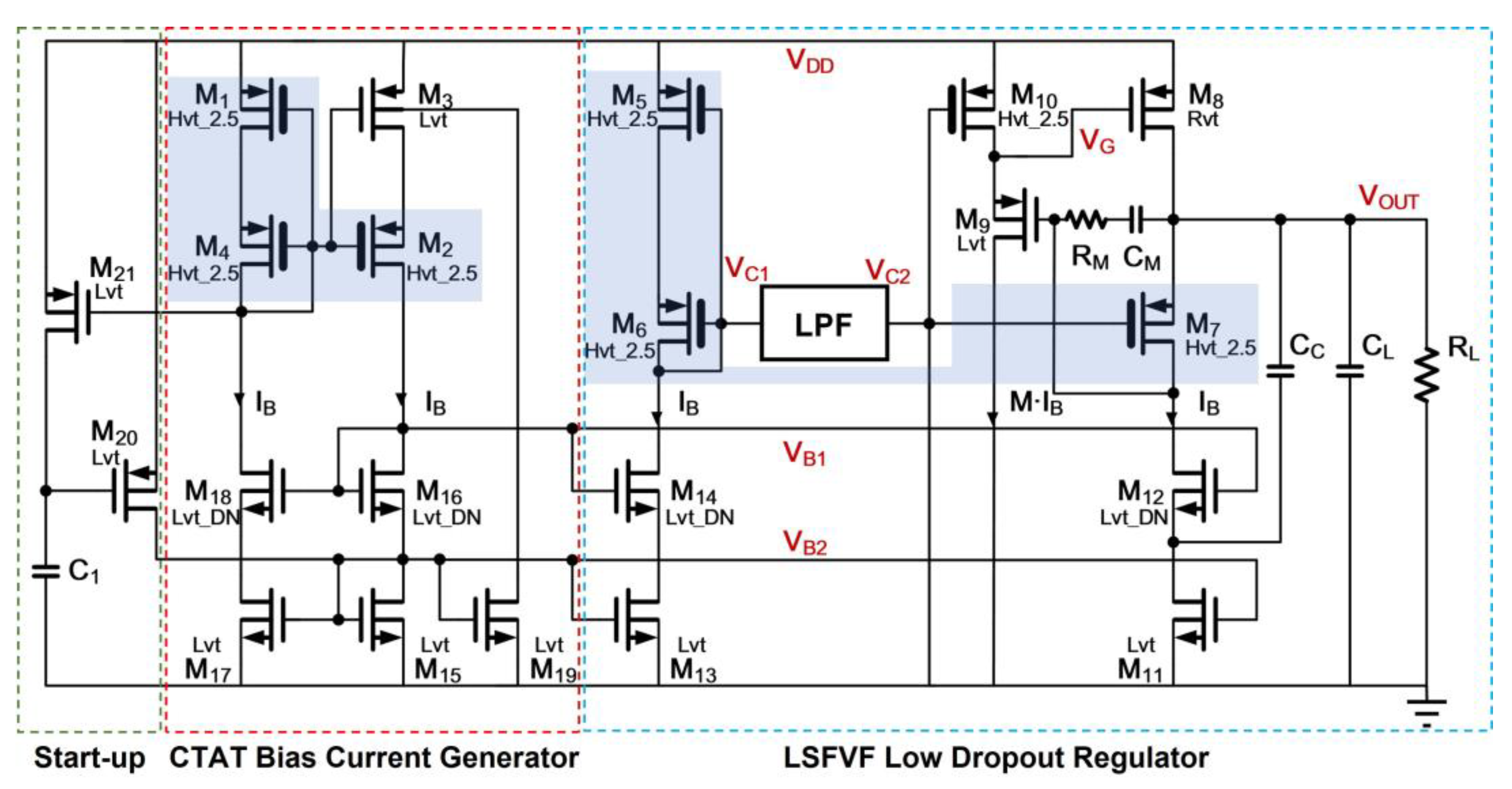
3. Proposed PSR Enhancer with PVT-Insensitive Dropout Voltage
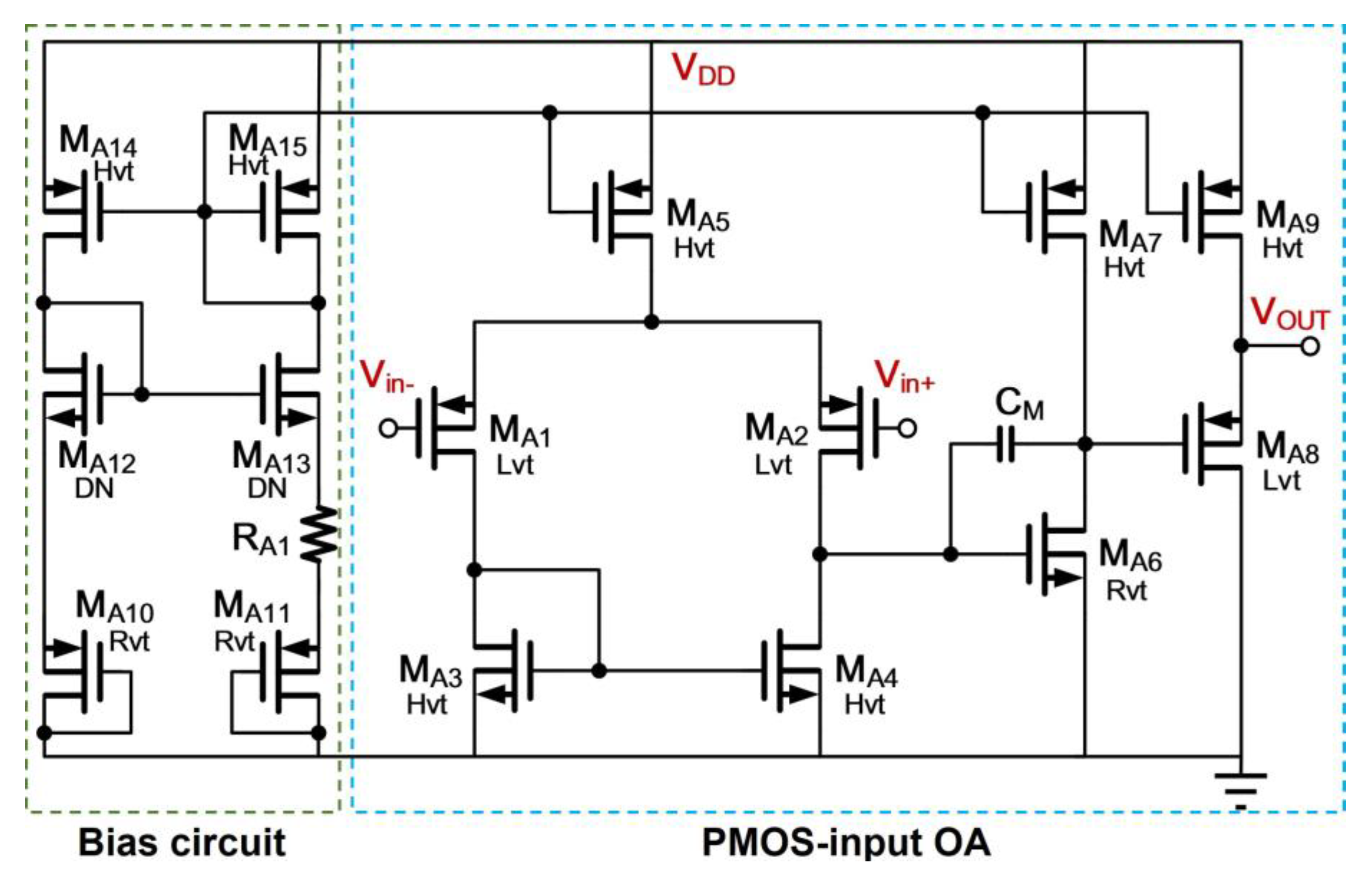
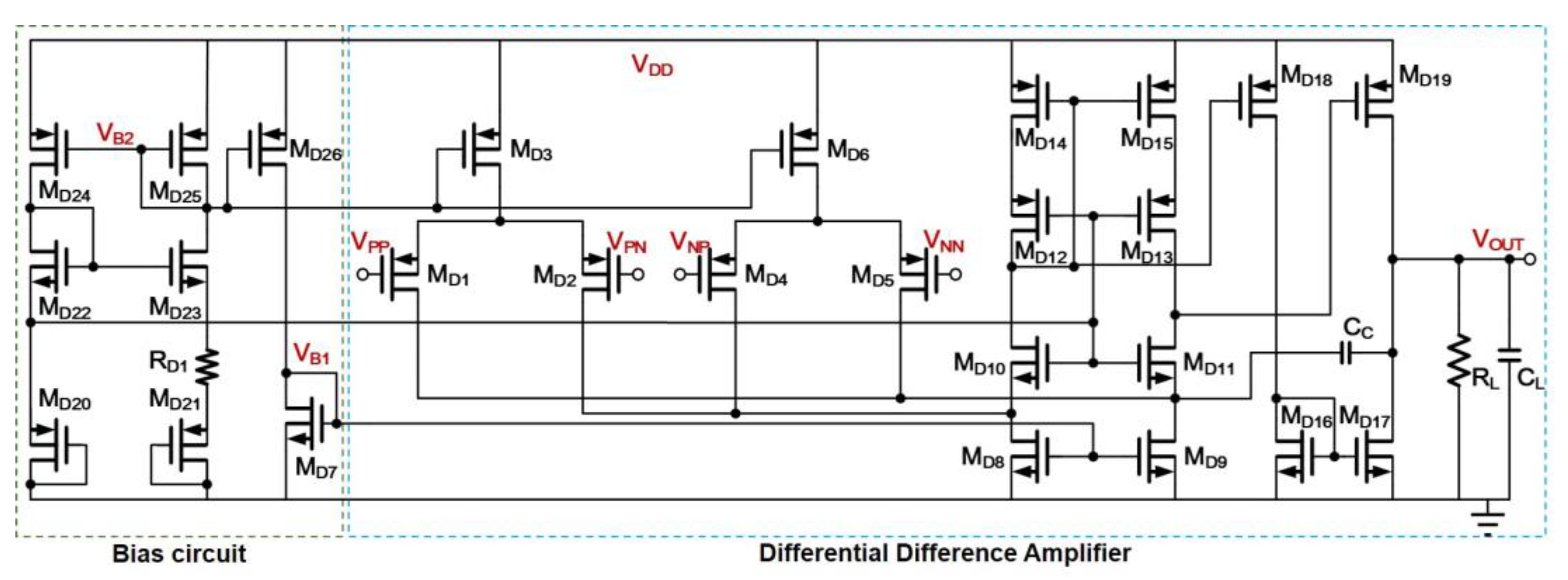
3.1. Proposed Enhancer Design
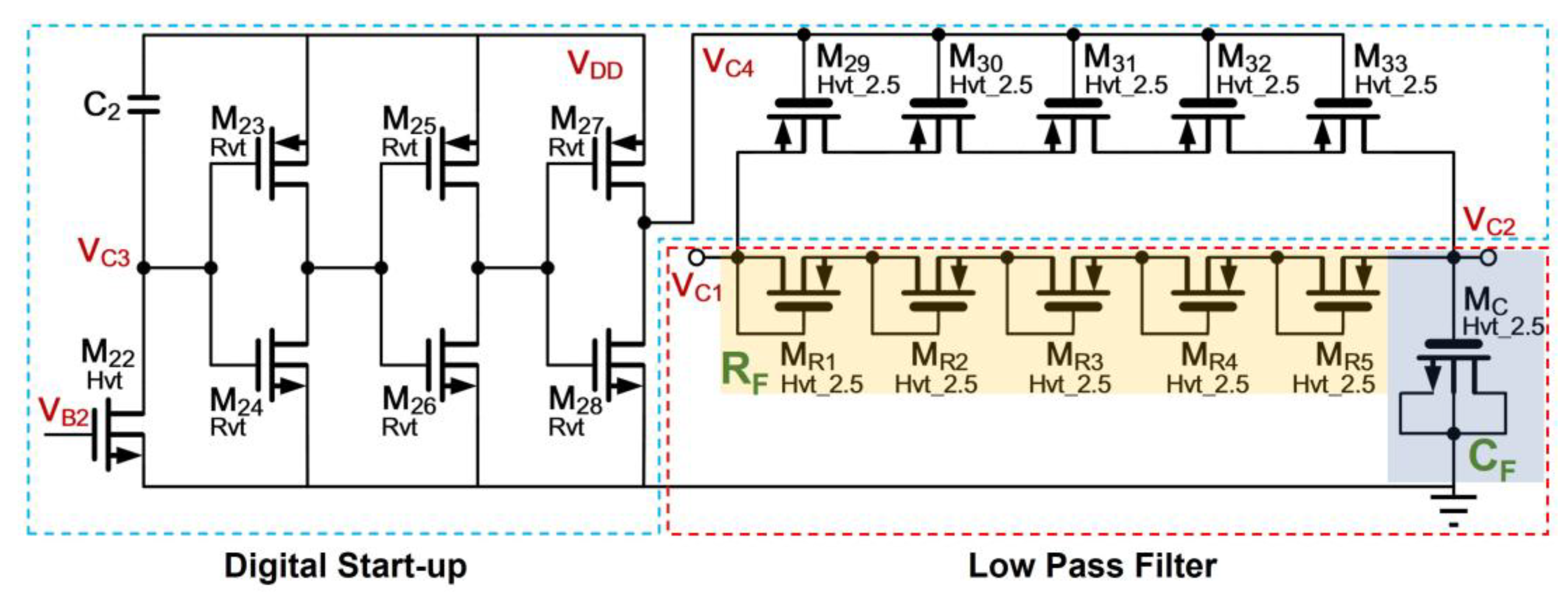
3.2. Low-Pass Filter in PSR Enhancer
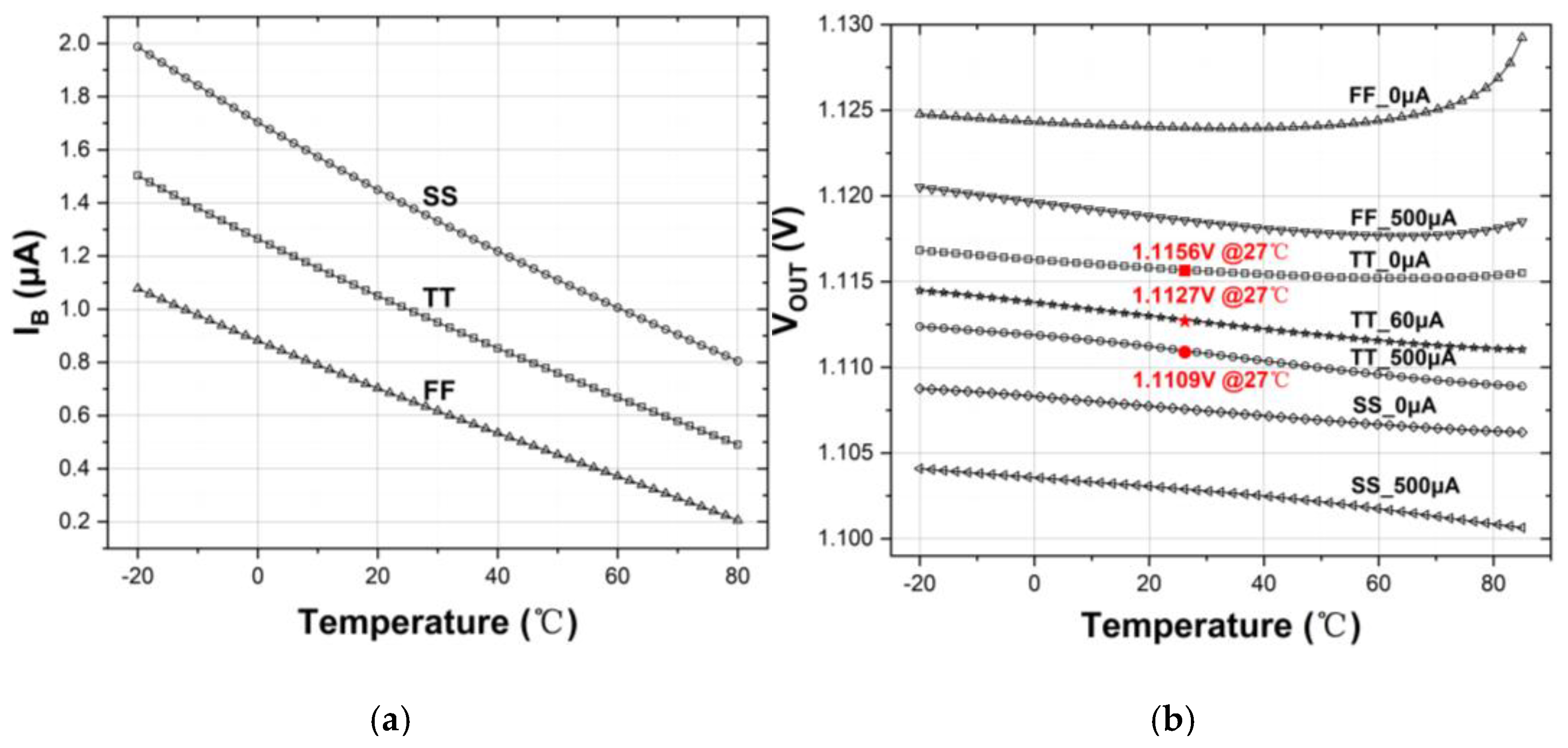
3.3. Temperature Analysis of the Building Blocks in PSR Enhancer
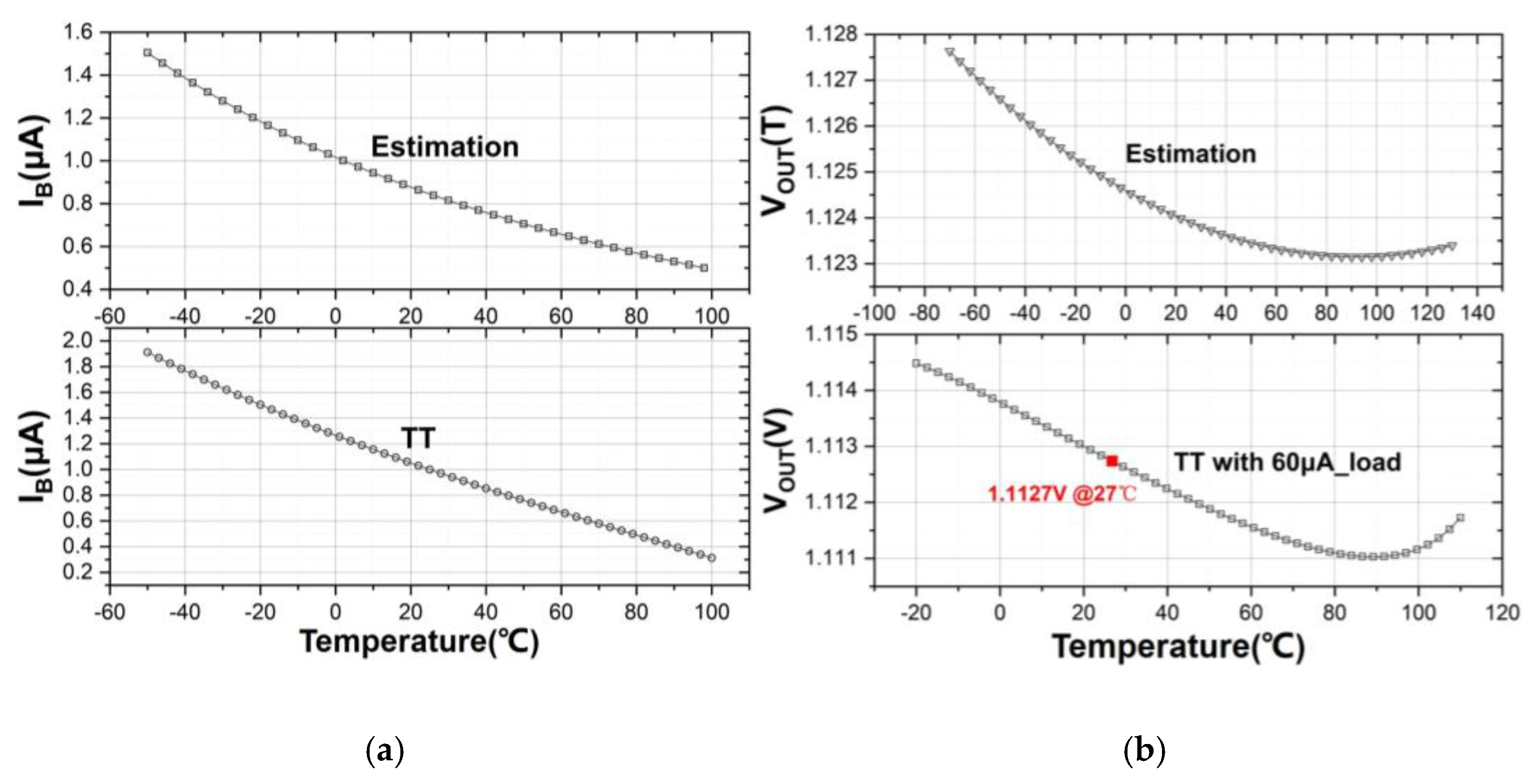
3.3.1. CTAT Biasing Current IB(T)
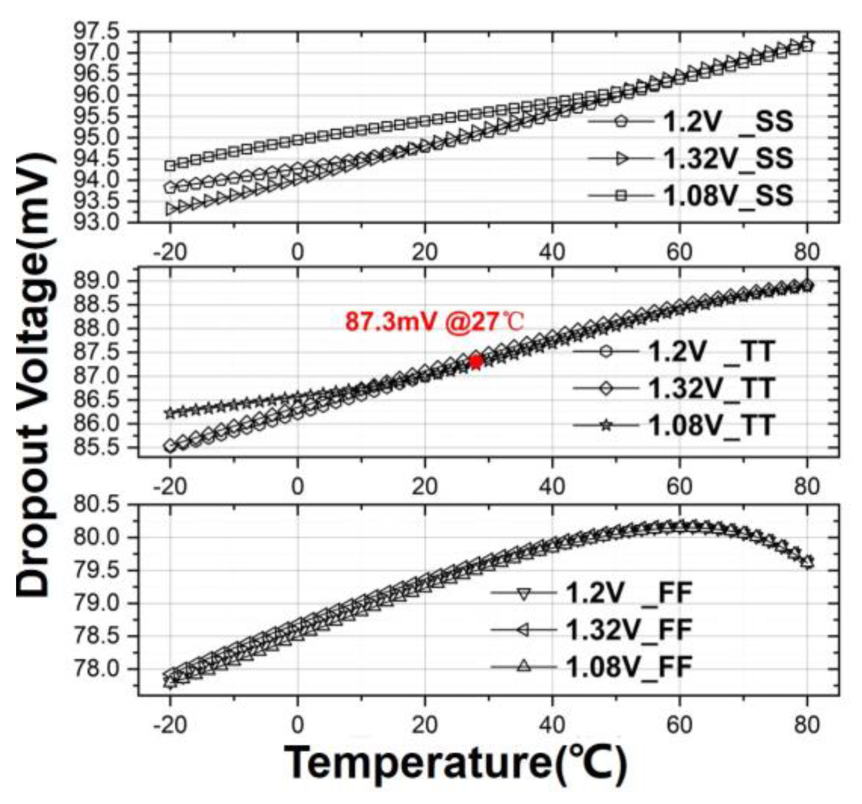
3.3.2. Temperature-Compensated VOUT(T) in LSFVF Topology
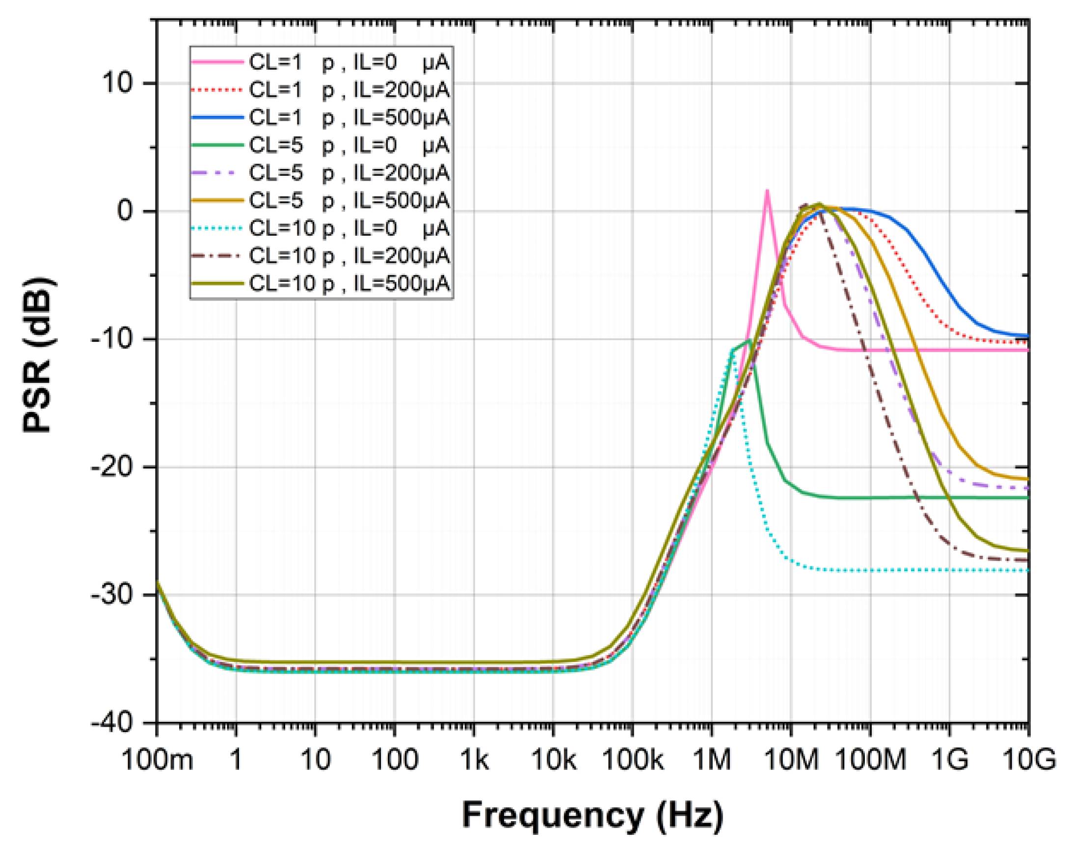
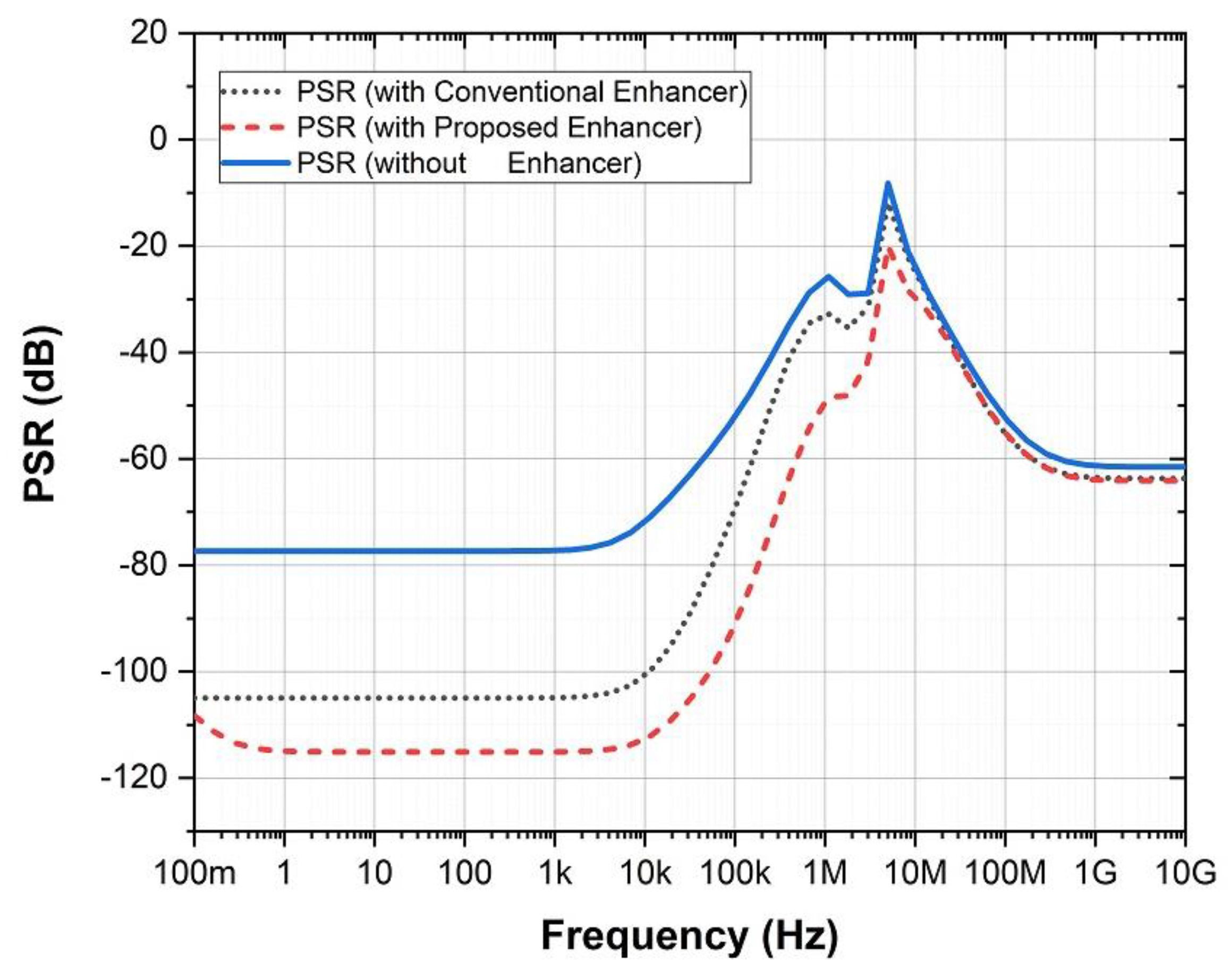
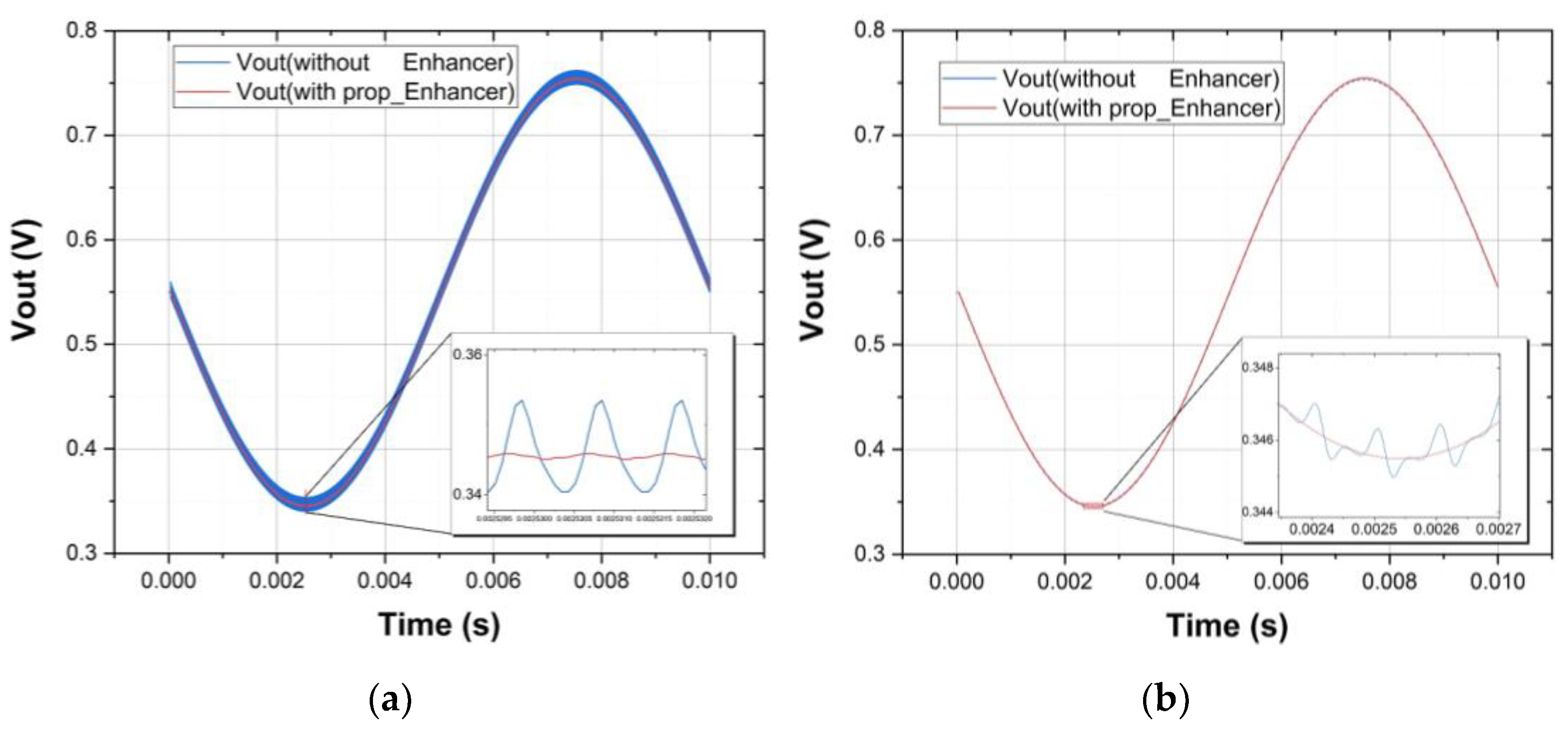
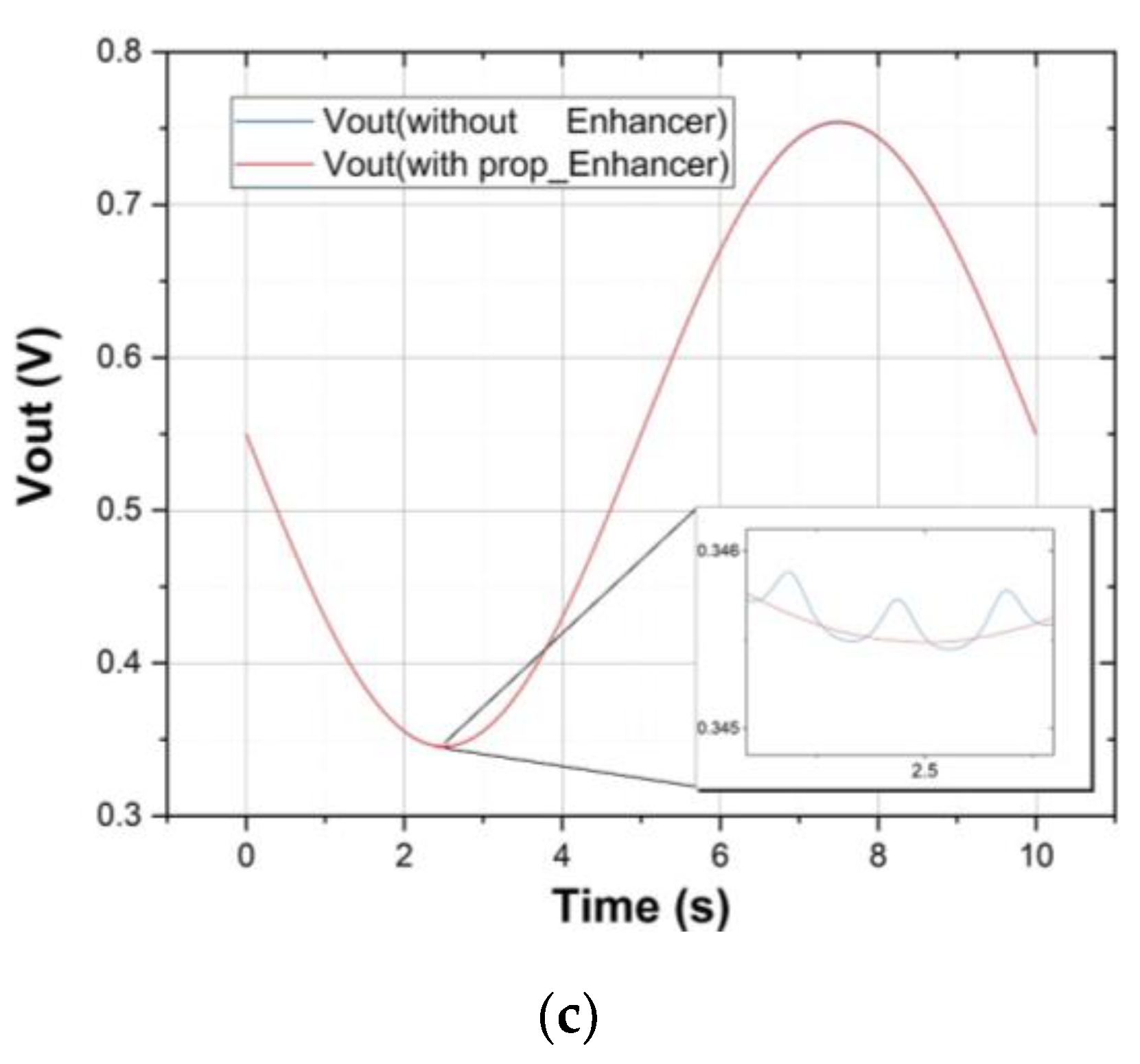
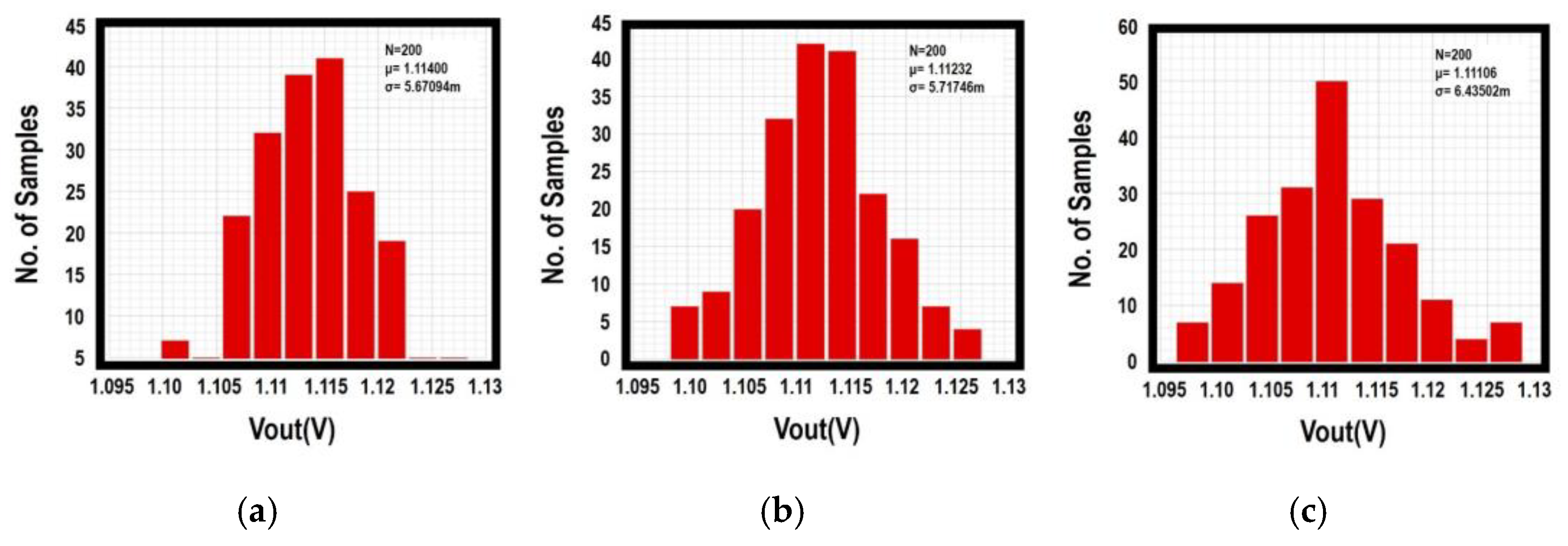
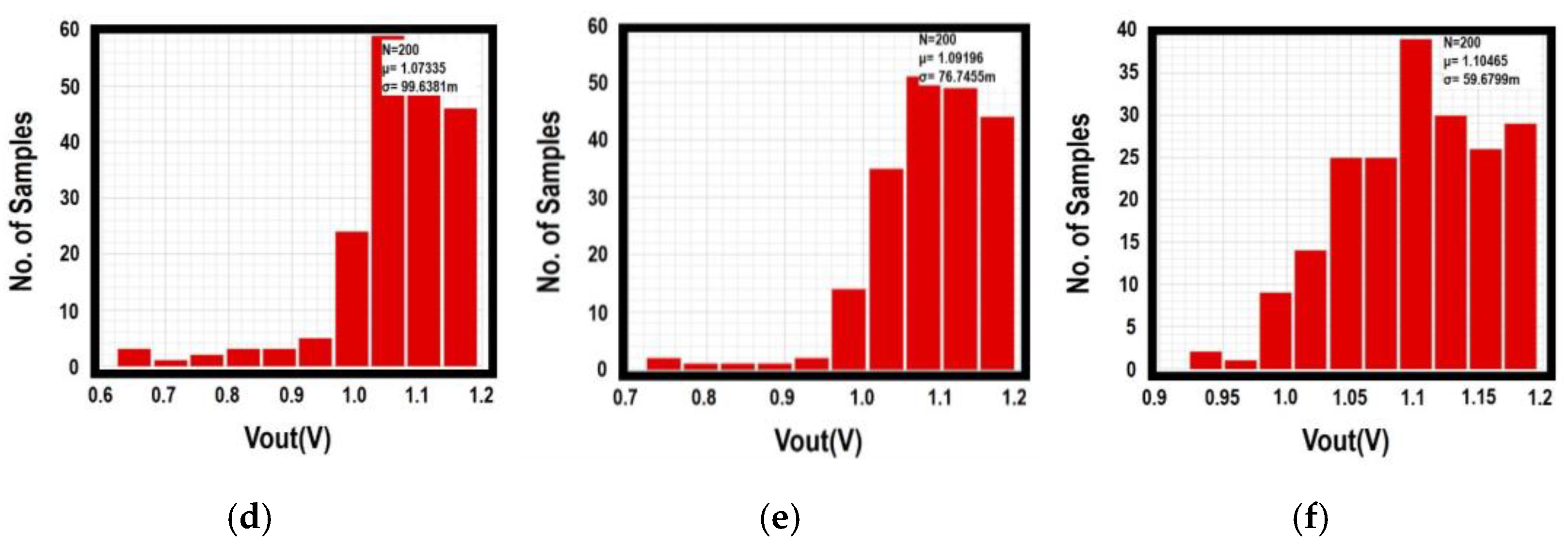
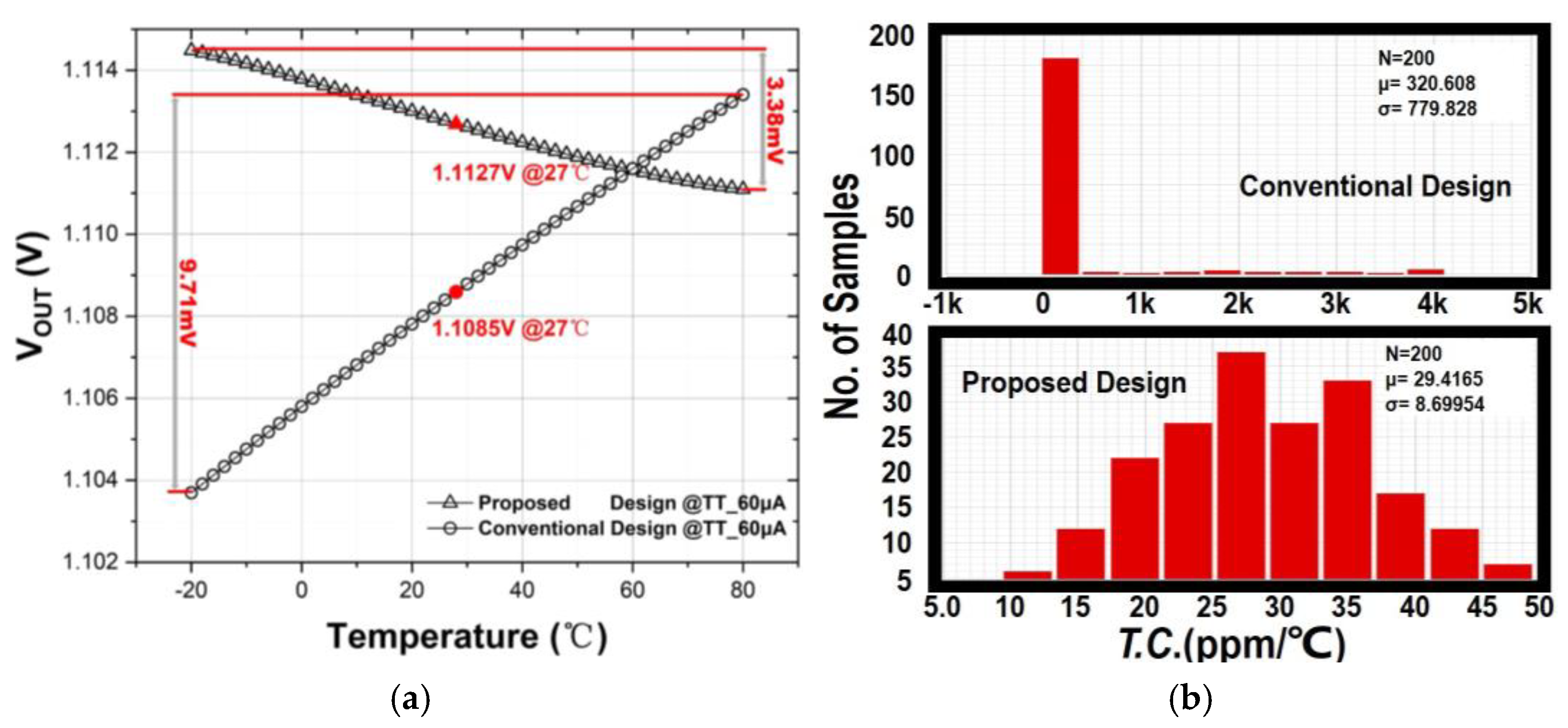
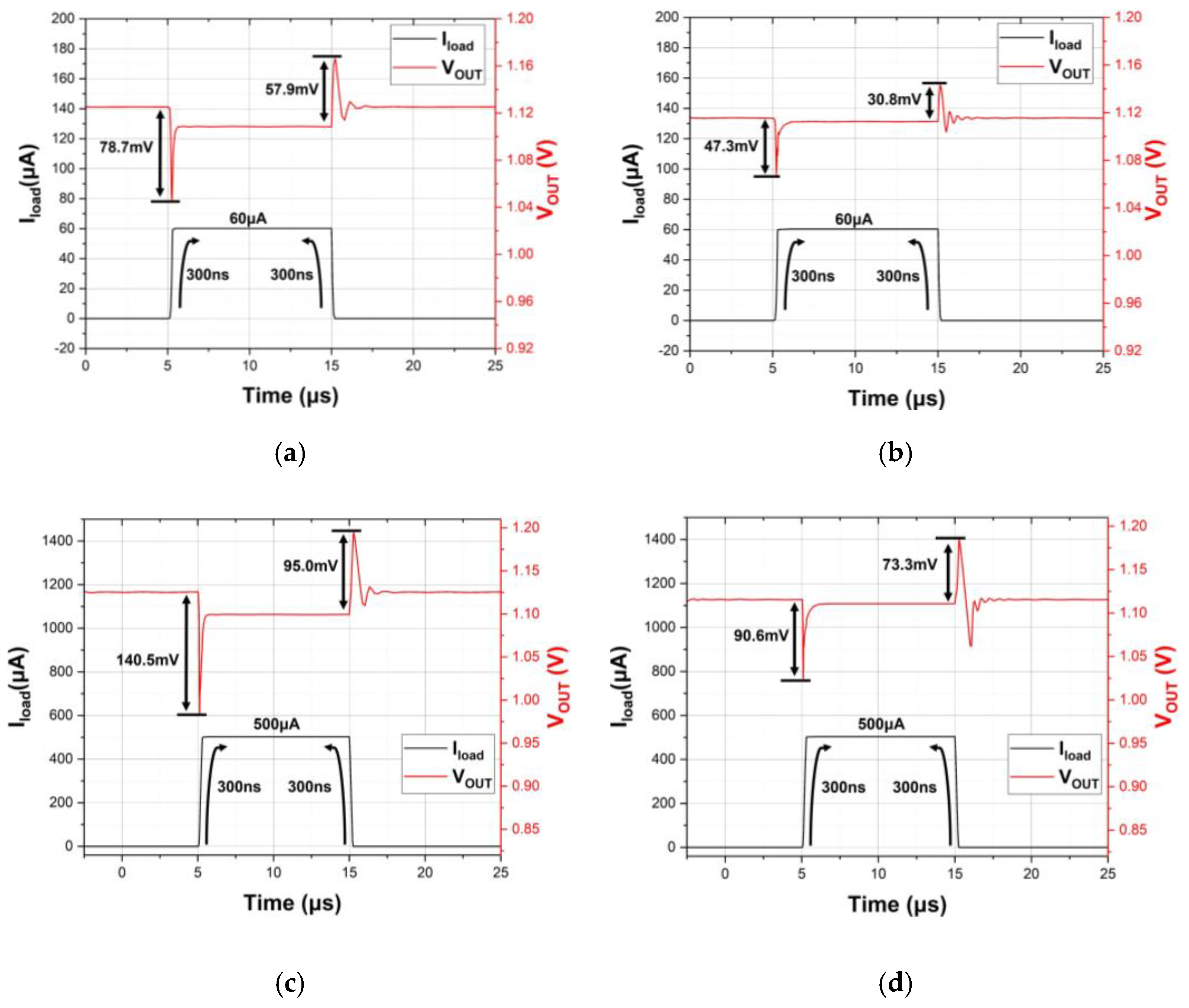
4. Results and Discussions
5. Conclusions
Author Contributions
Funding
Institutional Review Board Statement
Informed Consent Statement
Data Availability Statement
Conflicts of Interest
References
- Anand, T.; Makinwa, K.A.; Hanumolu, P.K. A VCO Based Highly Digital Temperature Sensor with 0.034 °C/mV Supply Sensitivity. IEEE J. Solid-State Circuits 2016, 51, 2651–2663. [Google Scholar] [CrossRef]
- Wei, J.; Li, X.; Sun, L.; Li, D. A 63.2μW 11-Bit Column Parallel Single-Slope ADC with Power Supply Noise Suppression for CMOS Image Sensors. In Proceedings of the 2020 IEEE International Symposium on Circuits and Systems (ISCAS), Seville, Spain, 12–14 October 2020; pp. 1–4. [Google Scholar]
- El Mehdi, B.; Mailly, F.; Latorre, L.; Nouet, P. Improvement of Power Supply Rejection Ratio in Wheatstone-bridge based piezoresistive MEMS. Analog Integr. Circ. Sig. Process. 2012, 71, 1–9. [Google Scholar] [CrossRef]
- Dumas, N.; Latorre, L.; Nouet, P. Analysis of offset and noise in CMOS piezoresistive sensors using a magnetometer as a case study. Sens. Actuators A Phys. 2006, 132, 14–20. [Google Scholar] [CrossRef]
- Li, Y.W.; Lakdawala, H. Smart integrated temperature sensor-mixed-signal circuits and systems in 32-nm and beyond. In Proceedings of the 2011 IEEE Custom Integrated Circuits Conference (CICC), San Jose, CA, USA, 19–21 September 2011; pp. 1–8. [Google Scholar]
- Tan, J.; Gläser, G. Supply sensitivity analysis for low-power time-domain temperature sensor in RFID application. In Proceedings of the 2017 IEEE International Conference on RFID Technology & Application (RFID-TA), Warsaw, Poland, 20–22 September 2017; pp. 196–201. [Google Scholar]
- Li, P.Z.; Lin, Y.T.; Lin, M.L.; Chiu, H.W. A wirelessly powered temperature sensor for cell culture micro system. In Proceedings of the 2017 International Conference on Applied System Innovation (ICASI), Sapporo, Japan, 13–17 May 2017; pp. 713–716. [Google Scholar]
- Arshad, M.M.; Hashim, U.; Choo, C.M. The Characterization of Power Supply Noise for Optical Mouse Sensor. In Proceedings of the 2006 Thirty-First IEEE/CPMT International Electronics Manufacturing Technology Symposium, Petaling Jaya, Malaysia, 8–10 November 2006; pp. 514–517. [Google Scholar]
- Ong, G.T.; Chan, P.K. A Low Quiescent Biased Regulator With High PSR Dedicated to Micropower Sensor Circuits. IEEE Sens. J. 2010, 10, 1266–1275. [Google Scholar] [CrossRef]
- Huab, M.J.D.; Alarcon, L.P.; Densing, C.V.J.; Maestro, R.J.M.; Rosales, M.D.; De Leon, M.T.G. Implementation of a maximum power point tracking system and an LDO regulator for interface circuits of solar energy harvesters for wireless sensor nodes. In Proceedings of the TENCON 2017-2017 IEEE Region 10 Conference, Penang, Malaysia, 5–8 November 2017; pp. 203–206. [Google Scholar]
- Kim, K.; Kim, J.H.; Gweon, S.; Lee, J.; Kim, M.; Lee, Y.; Kim, S.; Yoo, H.J. 22.3 A 0.5V 9.26 μW 15.28 mΩ/√Hz Bio-Impedance Sensor IC With 0.55° Overall Phase Error. In Proceedings of the 2019 IEEE International Solid-State Circuits Conference (ISSCC), San Francisco, CA, USA, 17–21 February 2019; pp. 364–366. [Google Scholar]
- Nasrollahpour, M.; Hamedi-Hagh, S.; Bastan, Y.; Amiri, P. ECP technique based capacitor-less LDO with high PSRR at low frequencies, −89dB PSRR at 1MHz and enhanced transient response. In Proceedings of the 2017 14th International Conference on Synthesis, Modeling, Analysis and Simulation Methods and Applications to Circuit Design (SMACD), Giardini Naxos, Italy, 12–15 June 2017; pp. 1–4. [Google Scholar]
- Ueno, K. CMOS Voltage and Current Reference Circuits consisting of Subthreshold MOSFETs-Micropower Circuit Components for Power-Aware LSI Applications. In Solid State Circuits Technologies; IntechOpen: Rijeka, Croatia, 2010. [Google Scholar]
- Gray, P.R.; Hurst, P.J.; Lewis, S.H.; Meyer, R.G. Analysis and Design of Analog Integrated Circuits, 5th ed.; John Wiley & Sons Inc.: Hoboken, NI, USA, 2010; pp. 315–321. [Google Scholar]
- Michejda, J.; Kim, S.K. A precision CMOS bandgap reference. IEEE J. Solid-State Circuits 1984, 19, 1014–1021. [Google Scholar] [CrossRef]
- Gupta, V.; Rincón-Mora, G.A.; Raha, P. Analysis and design of monolithic, high PSR, linear regulators for SoC applications. In Proceedings of the IEEE International SOC Conference, 2004. Proceedings, Santa Clara, CA, USA, 12–15 September 2004; pp. 311–315. [Google Scholar]
- Ahuja, B.K. An improved frequency compensation technique for CMOS operational amplifiers. IEEE J. Solid-State Circuits 1983, 18, 629–633. [Google Scholar] [CrossRef]
- Chen, H.; Leung, K.N. A fast-transient LDO based on buffered flipped voltage follower. In Proceedings of the 2010 IEEE International Conference of Electron Devices and Solid-State Circuits (EDSSC), Hong Kong, China, 15–17 December 2010; pp. 1–4. [Google Scholar]
- Harrison, R.R.; Charles, C. A low-power low-noise CMOS amplifier for neural recording applications. IEEE J. Solid-State Circuits 2003, 38, 958–965. [Google Scholar] [CrossRef]
- Man, T.Y.; Leung, K.N.A.; Leung, C.Y.; Mok, P.K.T.; Chan, M. Development of Single-Transistor-Control LDO Based on Flipped Voltage Follower for SoC. IEEE Trans. Circuits Syst. I Regul. Pap. 2008, 55, 1392–1401. [Google Scholar] [CrossRef] [Green Version]
- Blakiewicz, G. Output-capacitorless low-dropout regulator using a cascoded flipped voltage follower. IET Circuits Devices Syst. 2011, 5, 418–423. [Google Scholar] [CrossRef] [Green Version]
- Magnelli, L.; Crupi, F.; Corsonello, P.; Pace, C.; Iannaccone, G. A 2.6 nW, 0.45 V Temperature-Compensated Subthreshold CMOS Voltage Reference. IEEE J. Solid-State Circuits 2011, 46, 465–474. [Google Scholar] [CrossRef]
- Adl, A.H.; El-Sankary, K.; El-Masry, E. A high-order curvature compensation technique for bandgap voltage reference using subthreshold MOSFETs. Int. J. Electron. 2010, 97, 783–796. [Google Scholar] [CrossRef]
- Ferreira, L.H.; Pimenta, T.C.; Moreno, R.L. An Ultra Low-Voltage Ultra Low-Power CMOS Threshold Voltage Reference. IEICE Trans. 2007, 90, 2044–2050. [Google Scholar] [CrossRef]
- Zeghbroeck, B.V. Principles of Semiconductor Devices.; Online Textbook; University of Colorado: Denver, CO, USA, 2004; Chapter 2. [Google Scholar]
- Sackinger, E.; Guggenbuhl, W. A versatile building block: The CMOS differential difference amplifier. IEEE J. Solid-State Circuits 1987, 22, 287–294. [Google Scholar] [CrossRef]
- Guo, J.; Leung, K.N. A 6-μ W Chip-Area-Efficient Output-Capacitorless LDO in 90-nm CMOS Technology. IEEE J. Solid-State Circuits 2010, 45, 1896–1905. [Google Scholar] [CrossRef]


| Device | Size | Device | Size |
|---|---|---|---|
| M1 | 40/4 (μm/μm) | MB1,2 | 10/0.5 (μm/μm) |
| M2 | 320/4 (μm/μm) | MB3,4 | 10/2 (μm/μm) |
| MP | 1000/0.16 (μm/μm) | MB5 | 8.7/1 (μm/μm) |
| MA1,2 | 50/1 (μm/μm) | MB6,7 | 5.6/1 (μm/μm) |
| MA3,4 | 3/1 (μm/μm) | MB8,9 | 2/0.5 (μm/μm) |
| MA5 | 2/1 (μm/μm) | MB10,11 | 10/1 (μm/μm) |
| MA6 | 1.7/1 (μm/μm) | MB12,13 | 5/1 (μm/μm) |
| MA7 | 1.4/1 (μm/μm) | MB14,15 | 2/0.16 (μm/μm) |
| MA8 | 20/2 (μm/μm) | MB16,17 | 4/2 (μm/μm) |
| MA9 | 10/1 (μm/μm) | R1 | 283 kΩ |
| MA10,11 | 6/1 (μm/μm) | R2 | 99 kΩ |
| MA12,13 | 5/0.2 (μm/μm) | R3 | 283 kΩ |
| MA14,15 | 1/1 (μm/μm) | R4 | 515 kΩ |
| RA1 | 18.9 kΩ | R5 | 614 kΩ |
| RB1 | 27.8 kΩ | CM for OA1 | 0.8 pF |
| CC for OA2 | 0.4 pF |
| Device | Size | Device | Size |
|---|---|---|---|
| M1 | 1.7/0.3 (μm/μm) | M22 | 0.32/4 (μm/μm) |
| M2,4 | 20/0.3 (μm/μm) | M23,25,27 | 4/0.04 (μm/μm) |
| M3 | 2.1/4.5 (μm/μm) | M24,26,28 | 2/0.04 (μm/μm) |
| M5 | 3/0.3 (μm/μm) | M29–33 | 0.32/1 (μm/μm) |
| M6,7 | 14/0.3 (μm/μm) | MR1-R5 | 0.32/1 (μm/μm) |
| M8 | 1000/0.16 (μm/μm) | MC | 100/100 (μm/μm) |
| M9 | 10/0.1 (μm/μm) | RM | 5 kΩ |
| M10 | 1.9/0.3 (μm/μm) | C1 | 0.1 pF |
| M11,13,15,17 | 4/2 (μm/μm) | C2 | 1 pF |
| M12,14,16,18 | 5/1 (μm/μm) | CM | 1 pF |
| M19 | 0.12/5 (μm/μm) | CC | 2.5 pF |
| M20,21 | 1/0.3 (μm/μm) | CL | 1 pF–10 pF |
| Enhancer | Total Power | Bias Circuit | Power Output Stage | Additional Block |
|---|---|---|---|---|
| Proposed Work | 4.75 μA | 1.96 μA | 0.98 μA | None |
| Conventional Design | 4.75 μA | 1.96 μA | 0.98 μA | VREF Generator 8.67 μA |
| Supply Voltage | Power Consumption | RL | CL |
|---|---|---|---|
| 1.1 V | 60 μA | 100 kΩ | 30 pF |
| Open Loop Gain | PSR | CMRR | Bandwidth |
| 77.8 dB | −77.4 dB@1 Hz | 87.4 dB | 315 Hz |
| Unit Gain Frequency | Phase Margin | Input-Referred Noise | |
| 2.2 MHz | 69° | @1 kHz |
| Frequency | Without Enhancer | Conventional Enhancer | Proposed Enhancer |
|---|---|---|---|
| 1 Hz | −77 dB | −105 dB | −115 dB |
| 1 MHz | −26 dB | −32 dB | −50 dB |
| Conventional Design | This Work | |
|---|---|---|
| Process Technology | 40 nm CMOS | 40 nm CMOS |
| Power Transistor Size | PMOS (1 mm/160 nm) | PMOS (1 mm/160 nm) |
| Current Consumption IQ (μA) | 4.75 | 4.75 |
| Supply Voltage (V) | 1.2 | 1.2 |
| VOUT @60 μA_Load (V) | 1.1085 | 1.1127 |
| Minimum ILOAD, min (μA) | 0 | 0 |
| Maximum ILOAD, max (μA) | 500 | 500 |
| ΔILOAD (μA) | 500 | 500 |
| Voltage Reference Required | Yes | No |
| Op-amp Required | Yes | No |
| ΔVOUT (−20–80 °C) (mV) | 9.71 1 | 3.38 1 |
| PSR Bandwidth (kHz) | 65.5 | 107.2 |
| PSR @ 1 Hz, 1 MHz (dB) Mean of VOUT (V), 200 samples | −31.6, −8.1 1.0920 | −36.0, −20.2 1.1123 |
| SD of VOUT (mV), 200 samples | 76.7 | 5.72 |
| T.C. (1 sample @nominal) (ppm/°C) | 87.60 1 | 30.38 1 |
| Mean T.C. (200 samples) (ppm/°C) SD T.C. (200 samples) (ppm/°C) | 320.6 2 779.8 | 29.4 2 8.7 |
| Process Sensitivity for VOUT | 7.028% | 0.514% |
| Edge Time (μs) ΔVOUT (mV) @500 μA | 0.3 140.5 | 0.3 90.6 |
| Edge Time Ratio K | 1 | 1 |
| FOM3 [27] (mV) | 1.33475 | 0.86070 |
Publisher’s Note: MDPI stays neutral with regard to jurisdictional claims in published maps and institutional affiliations. |
© 2021 by the authors. Licensee MDPI, Basel, Switzerland. This article is an open access article distributed under the terms and conditions of the Creative Commons Attribution (CC BY) license (https://creativecommons.org/licenses/by/4.0/).
Share and Cite
Zhang, J.; Chan, P.K. A CMOS PSR Enhancer with 87.3 mV PVT-Insensitive Dropout Voltage for Sensor Circuits. Sensors 2021, 21, 7856. https://doi.org/10.3390/s21237856
Zhang J, Chan PK. A CMOS PSR Enhancer with 87.3 mV PVT-Insensitive Dropout Voltage for Sensor Circuits. Sensors. 2021; 21(23):7856. https://doi.org/10.3390/s21237856
Chicago/Turabian StyleZhang, Jianyu, and Pak Kwong Chan. 2021. "A CMOS PSR Enhancer with 87.3 mV PVT-Insensitive Dropout Voltage for Sensor Circuits" Sensors 21, no. 23: 7856. https://doi.org/10.3390/s21237856