
BPF-Based Thermal Sensor Circuit for On-Chip Testing of RF Circuits

 , , ,
, , , 
Abstract
:1. Introduction
2. Sensor Description and Design
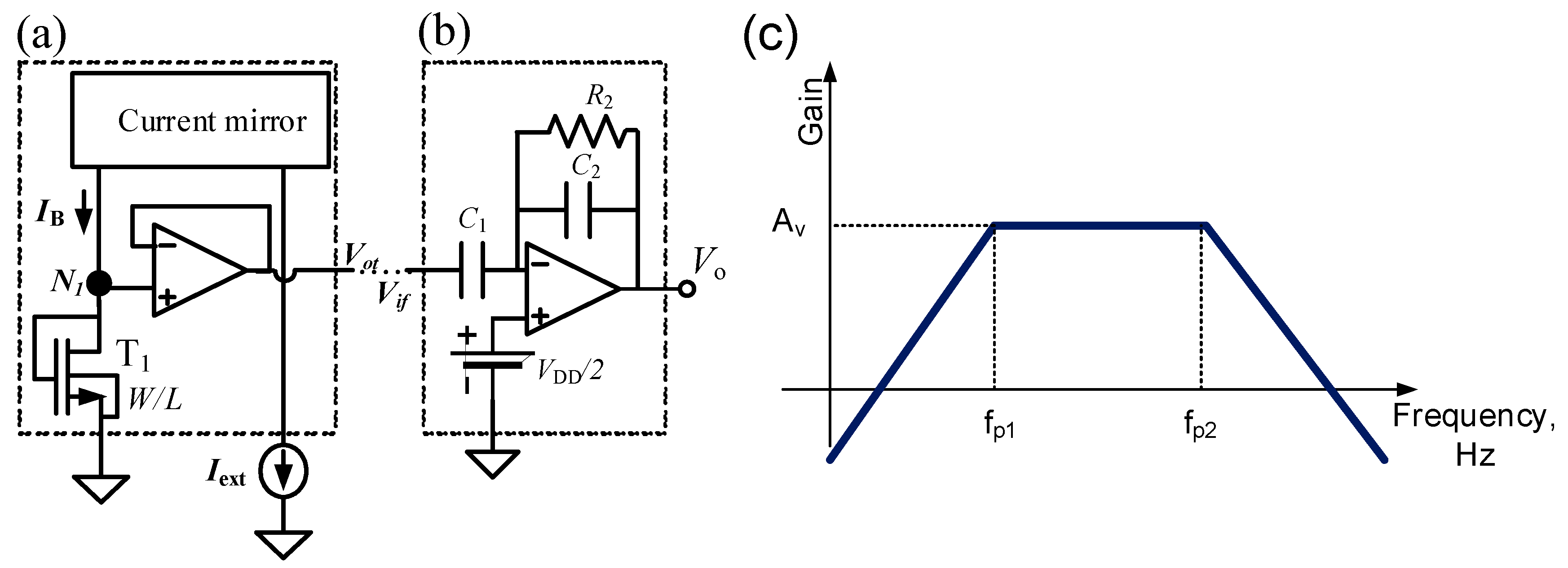
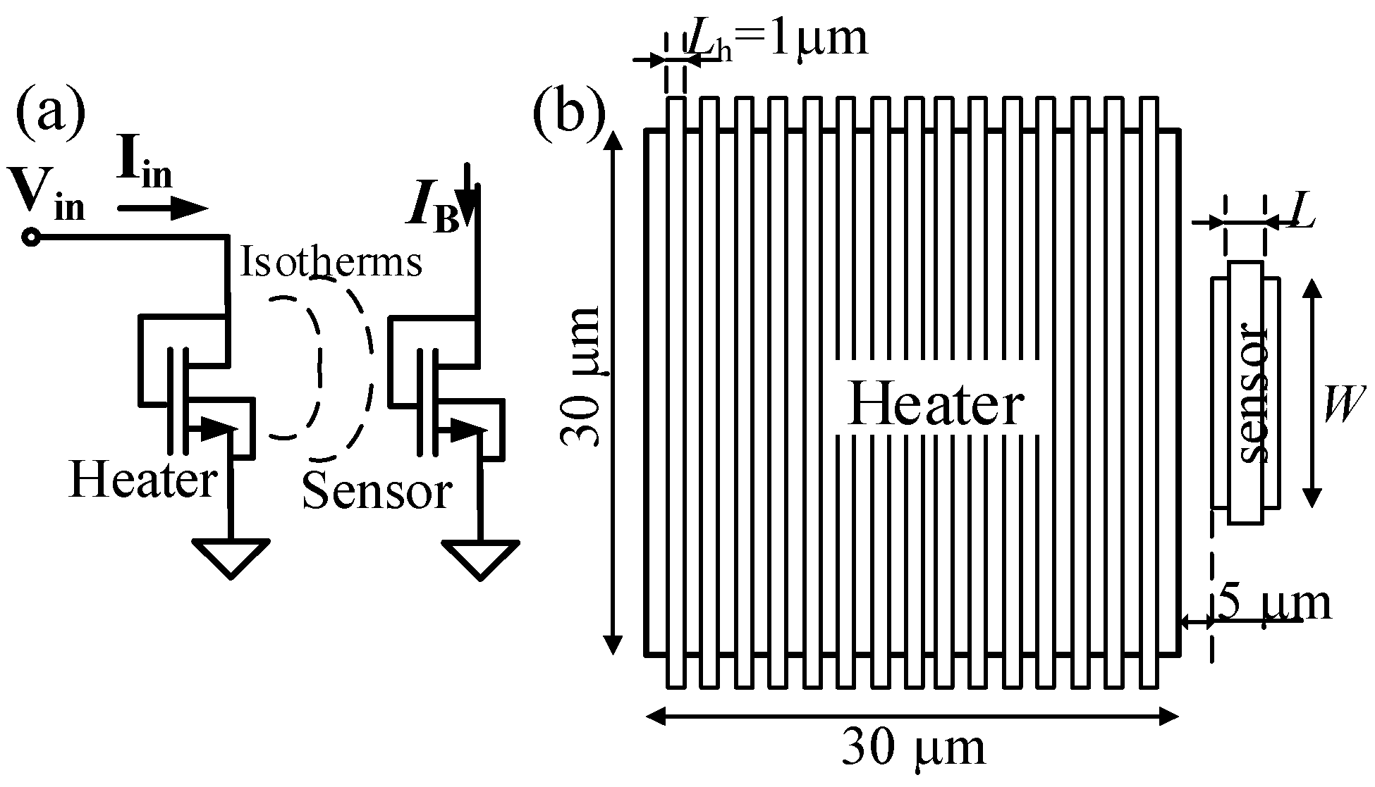
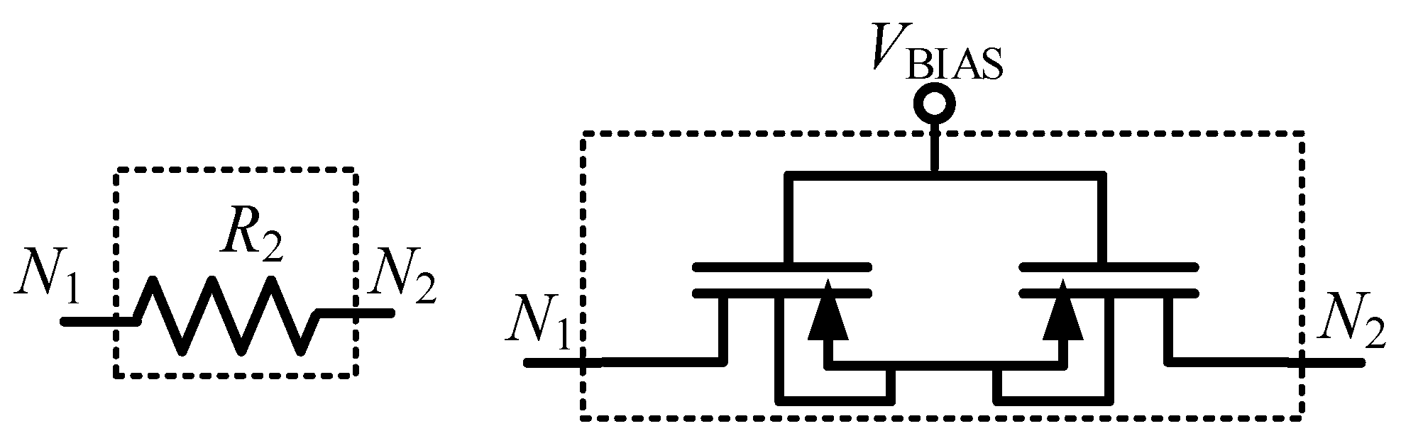
2.1. Temperature Transducer Description
2.2. Band Pass Filter Amplifier: Noise and Linearity Analysis
3. Sensor Implementation and Validation
3.1. Temperature Transducer
3.2. Band Pass Filter Amplifier
3.3. Overall Sensor Characterization
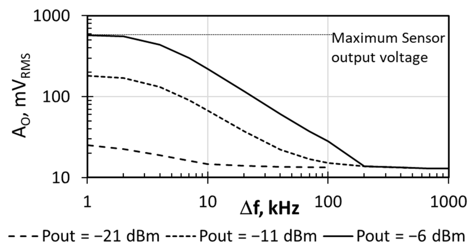
4. Use Case: RF Tuned Class-A Power Amplifier Monitoring
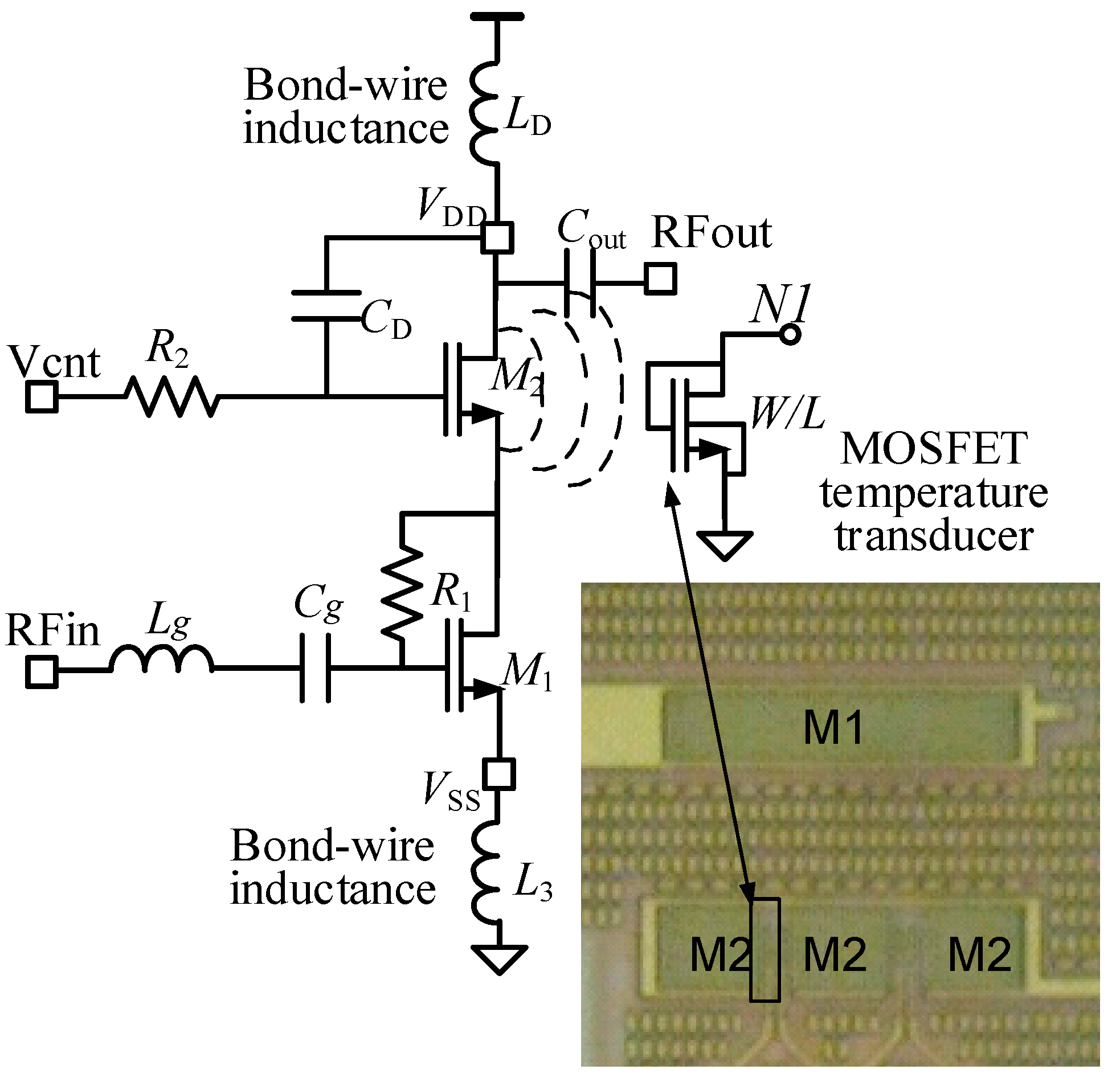
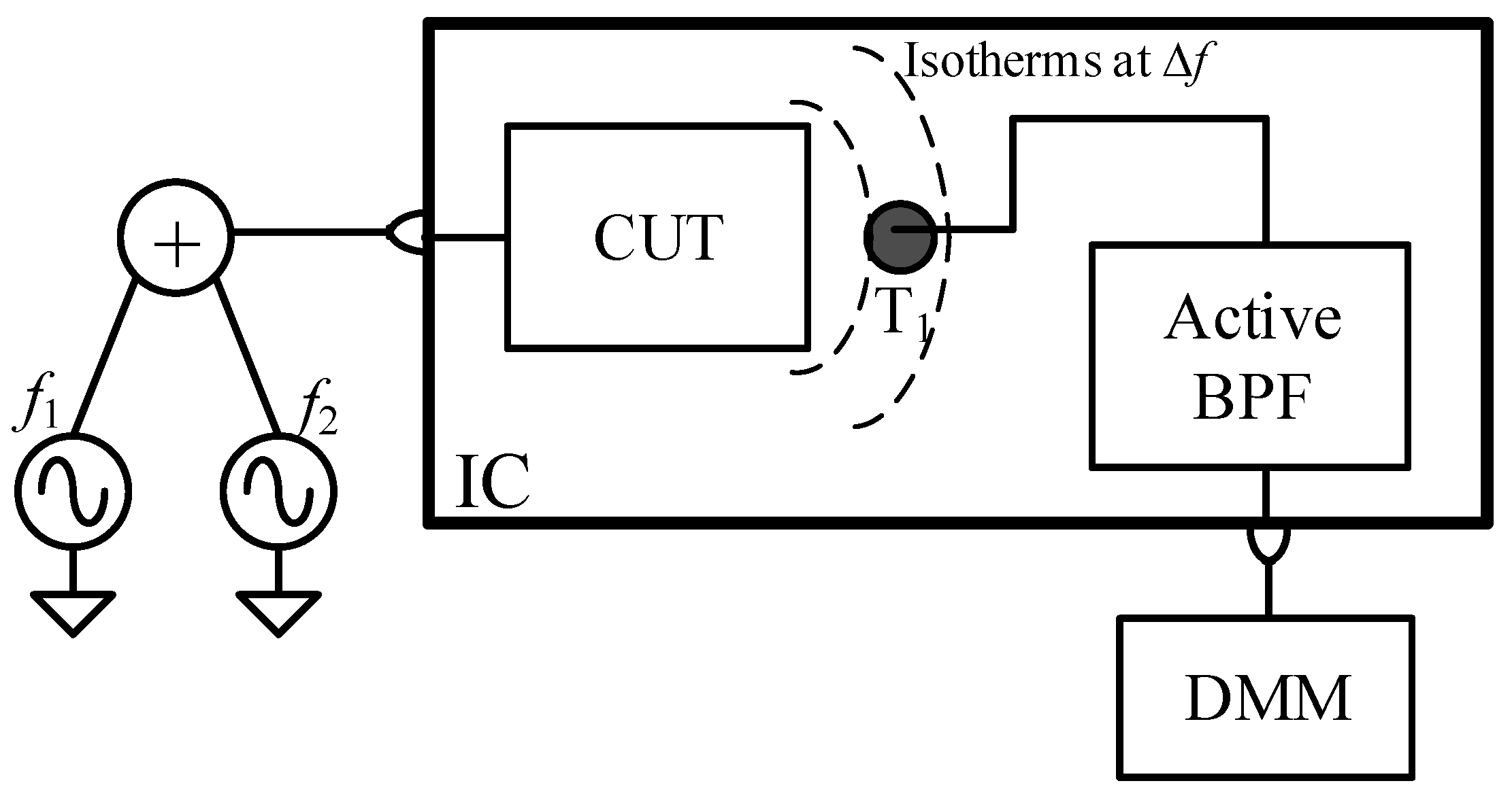
4.1. Circuit and Experimental Set Up Description
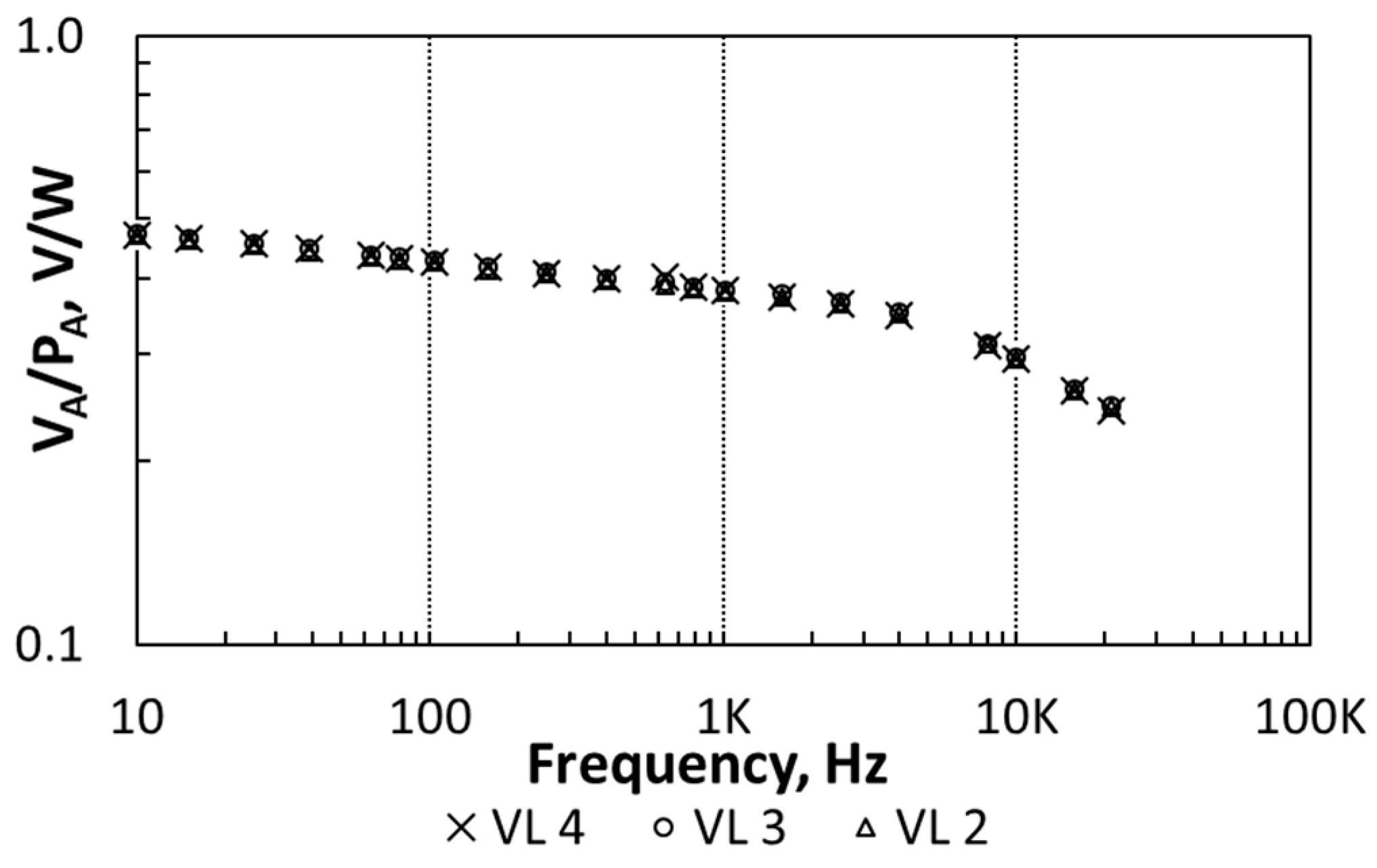
4.2. Output Power Monitoring
4.3. Central Frequency Monitoring
5. Conclusions
6. Patents
Author Contributions
Funding
Data Availability Statement
Acknowledgments
Conflicts of Interest
References
- Altet, J.; Claeys, W.; Dilhaire, S.; Rubio, A. Dynamic surface temperature measurements in ICs. Proc. IEEE 2006, 94, 1519–1533. [Google Scholar] [CrossRef]
- Soden, J.J.; Anderson, R.E. IC failure analysis: Techniques and tools for quality reliability improvement. Proc. IEEE 1993, 81, 703–715. [Google Scholar] [CrossRef]
- Perpiñà, X.; Vellvehi, M.; Jordà, X. Chapter 13: Thermal issues in microelectronics. In Thermometry at the Nanoscale: Techniques and Selected Applications, 1st ed.; Nanoscience & Nanotechnology Series; Carlos, L., Palacio, F., Eds.; The Royal Society of Chemistry: Cambridge, UK, 2016. [Google Scholar]
- Hamann, H.F.; Weger, A.; Lacey, J.A.; Hu, Z.; Bose, P.; Cohen, E.; Wakil, J. Hotspot-limited microprocessors: Direct temperature and power distribution measurements. J. Solid State-Circuits 2007, 42, 56–65. [Google Scholar] [CrossRef]
- Perpiñà, X.; Jordà, X.; Vellvehi, M.; Altet, J. Study of heat sources interacting in integrated circuits by laser mirage effect. Appl. Phys. Lett. 2014, 105, 084101. [Google Scholar] [CrossRef]
- Arumi, D.; Rodriguez-Montanes, R.; Figueras, J.; Eichenberger, S.; Hora, C.; Kruseman, B.; Lousberg, M.; Majhi, A.K. Diagnosis of bridging defects based on current signatures at low power supply voltages. In Proceedings of the 25th IEEE VLSI Test Symposium (VTS’07), Berkeley, CA, USA, 6–10 May 2007; pp. 145–150. [Google Scholar] [CrossRef]
- Segura, J.; Rubio, A. A detailed analysis of CMOS SRAMs with gate oxide short defects. J. Solid State-Circuits 1997, 21, 1543–1550. [Google Scholar] [CrossRef]
- Lai, J.; Chandrachood, M.; Majumda, A.; Carrejo, J.P. Thermal detection of device failure by atomic force microscopy. IEEE Electron. Device Lett. 1995, 16, 312–315. [Google Scholar] [CrossRef]
- Bianic, S.; Allemand, S.; Kerrosa, G.; Scafidi, P.; Renard, D. Advanced backside failure analysis in 65 nm CMOS technology. Microelectron. Reliab. 2007, 47, 1550–1554. [Google Scholar] [CrossRef]
- Mahajan, R.; Chiu, C.; Chrysler, G. Cooling a microprocessor chip. Proc. IEEE 2006, 94, 1476–1486. [Google Scholar] [CrossRef]
- Chouhan, S.S.; Halonen, K. A low power temperature to frequency converter for the on-chip temperature measurement. IEEE Sens. J. 2015, 15, 4234–4240. [Google Scholar] [CrossRef] [Green Version]
- Lo, Y.L.; Chiu, Y.-T. A high-accuracy, high-resolution, and low-cost all-digital temperature sensor using a voltage compensation ring oscillator. IEEE Sens. J. 2016, 16, 43–52. [Google Scholar] [CrossRef]
- Chen, P.-Y.; Huang, G.-Y.; Shyu, Y.-T.; Chang, S.-J. A primary-auxiliary temperature sensing scheme for multiple hotspots in system-on-a-chips. IEEE Sens. J. 2014, 14, 2633–2642. [Google Scholar] [CrossRef]
- Yang, T.; Kim, S.; Kinget, P.R.; Seok, M. Compact and supply-voltage-scalable temperature sensors for dense on-chip thermal monitoring. J. Solid State-Circuits 2015, 50, 2773–2785. [Google Scholar] [CrossRef]
- An, Y.J.; Ryu, K.; Jung, D.-H.; Woo, S.-H.; Jung, S.-O. An energy efficient time-domain temperature sensor for low-power on-chip thermal management. IEEE Sens. J. 2014, 14, 104–110. [Google Scholar] [CrossRef]
- Shor, J. Compact thermal sensors for dense cpu thermal monitoring and regulation: A review. IEEE Sens. J. 2020. [Google Scholar] [CrossRef]
- Eberlein, M.; Pretl, H. A No-Trim, Scaling-Friendly Thermal Sensor in 16 nm FinFET using bulk diodes as sensing elements. IEEE Solid-State Circuits Lett. 2019, 2, 63–66. [Google Scholar] [CrossRef]
- Bass, O.; Shor, J. A miniaturized 0.003 mm2 PNP-based thermal sensor for dense CPU thermal monitoring. IEEE Trans. Circuits Syst. I Reg. Pap. 2020, 67, 2984–2992. [Google Scholar] [CrossRef]
- Perpiñà, X.; Werkhoven, R.J.; Vellvehi, M.; Jakovenko, J.; Jordà, X.; Kunen, J.M.G.; Bancken, P.; Bolt, P.J. Thermal analysis of LED lamps for optimal driver integration. IEEE Trans. Power Electron. 2015, 30, 3876–3891. [Google Scholar] [CrossRef]
- Vellvehi, M.; Perpinya, X.; Leon, J.; Avino-Salvado, O.; Ferrer, C.; Jordà, X. Local thermal resistance extraction in monolithic microwave integrated circuits. IEEE Trans. Ind. Electron 2020. [Google Scholar] [CrossRef]
- Rodriguez, R.; Crespo-Yepes, A.; Martin-Martinez, J.; Nafria, M.; Aragones, X.; Mateo, D.; Barajas, E. Experimental monitoring of aging in CMOS RF linear power amplifiers: Correlation between device and circuit degradation. In Proceedings of the 2020 IEEE International Reliability Physics Symposium (IRPS), Dallas, TX, USA, 28 April–30 May 2020; pp. 1–7. [Google Scholar] [CrossRef]
- Crespo-Yepes, A.; Barajas, E.; Martin-Martinez, J.; Mateo, D.; Aragones, X.; Rodriguez, R.; Nafria, M. MOSFET degradation dependence on input signal power in a RF power amplifier. Microelectron. Eng. 2017, 178, 289–292. [Google Scholar] [CrossRef] [Green Version]
- Yuan, J.S.; Xu, Y.; Yen, S.D.; Bi, Y.; Hwang, G.W. Hot carrier injection stress effect on a 65 nm LNA at 70 GHz. IEEE Trans. Device Mater. Rel. 2014, 14, 931–934. [Google Scholar] [CrossRef]
- Simicic, M.; Weckx, P.; Parvais, B.; Roussel, P.; Kaczer, B.; Gielen, G. Understanding the impact of time-dependent random variability on analog ICs: From single transistor measurements to circuit simulations. IEEE Trans. Very Large Scale Integr. (VLSI) Syst. 2019, 27, 601–610. [Google Scholar] [CrossRef]
- Yen, H.D.; Yuan, J.S.; Huang, G.W.; Yeh, W.K.; Huang, F.S. Reliability performance of a 70-GHz mixer in 65-nm technology. IEEE Trans. Device Mater. Rel. 2016, 16, 101–104. [Google Scholar] [CrossRef]
- Vinaya, M.M.; Paily, R.; Mahanta, A. A new PVT compensation technique based on current comparison for low-voltage, near sub-threshold LNA. IEEE Trans. Circuits Syst. I Reg. Pap. 2015, 62, 2908–2919. [Google Scholar] [CrossRef]
- Barabino, N.; Silveira, F. Digitally assisted CMOS RF detectors with self-calibration for variability compensation. IEEE Trans. Microw. Theory Techn. 2015, 63, 1676–1682. [Google Scholar] [CrossRef]
- Wursthorn, J.; Knapp, H.; Al-Eryani, J.; Aufinger, K.; Maurer, L. Absolute mm-wave power sensor using a switching quad output stage. In Proceedings of the 2017 IEEE 17th Topical Meeting on Silicon Monolithic Integrated Circuits in RF Systems (SiRF), Phoenix, AZ, USA, 15–18 January 2017; pp. 40–42. [Google Scholar] [CrossRef]
- Onabajo, M.; Silva-Martinez, J. Analog Circuit Design for Process. Variation-Resilient System-on-a-Chip, 1st ed.; Springer: New York, NY, USA, 2012. [Google Scholar] [CrossRef]
- Bowers, S.M.; Sengupta, K.; Dasgupta, K.; Parker, B.D.; Hajimiri, A. Integrated self-healing for mm-wave power amplifiers. IEEE Trans. Microw. Theory Tech. 2013, 61, 1301–1315. [Google Scholar] [CrossRef]
- Perpiñà, X.; León, J.; Altet, J.; Vellvehi, M.; Reverter, F.; Barajas, E.; Jordà, X. Thermal phase lag heterodyne infrared imaging for current tracking in radio frequency integrated circuits. Appl. Phys. Lett. 2017, 110, 094101. [Google Scholar] [CrossRef] [Green Version]
- Perpiñà, X.; Reverter, F.; León, J.; Barajas, E.; Vellvehi, M.; Jordà, X.; Altet, J. Output power and gain monitoring in RF CMOS class A power amplifiers by thermal imaging. IEEE Trans. Instrum. Meas. 2019, 68, 2861–2870. [Google Scholar] [CrossRef] [Green Version]
- Aldrete, E.; Mateo, D.; Altet, J.; Salhi, M.A.; Grauby, S.; Dilhaire, S.; Onabajo, M.; Silva-Martinez, J. Strategies for built-in characterization testing and performance monitoring of analog RF circuits with temperature measurements. Meas. Sci. Technol. 2010, 21, 075104. [Google Scholar] [CrossRef]
- Altet, J.; Gómez, D.; Perpiñà, X.; Mateo, D.; González, J.L.; Vellvehi, M.; Jordà, X. Efficiency determination of RF linear power amplifiers by steady-state temperature monitoring using built-in sensors. Sens. Act. A Phys. 2013, 192, 49–57. [Google Scholar] [CrossRef]
- Altet, J.; Mateo, D.; Gómez, D.; González, J.L.; Martineau, B.; Siligaris, A.; Aragones, X. Temperature sensors to measure the central frequency and 3 dB bandwidth in mmW power amplifiers. IEEE Microw. Wirel. Compon. Lett. 2014, 24, 272–274. [Google Scholar] [CrossRef]
- Onabajo, M.; Gómez, D.; Aldrete, E.; Altet, J.; Mateo, D.; Silva-Martinez, J. Survey of robustness enhancement techniques for wireless systems-on-a-chip and study of temperature as observable for process variations. J. Electron. Test. 2011, 27, 225–240. [Google Scholar] [CrossRef] [Green Version]
- Onabajo, M.; Altet, J.; Aldrete, E.; Mateo, D.; Silva-Martinez, J. Electrothermal design procedure to observe RF circuit power and linearity characteristics with homodyne differential temperature sensor. IEEE Trans. TCAS I 2011, 58, 458–469. [Google Scholar] [CrossRef]
- Abdallah, L.; Stratigopoulos, H.; Mir, S.; Altet, J. Defect-oriented non-intrusive RF test using on-chip temperature sensors. In Proceedings of the 31st IEEE VTS, Berkeley, CA, USA, 29 April–2 May 2013. [Google Scholar] [CrossRef]
- Altet, J.; Rubio, A.; Rossello, J.L.; Segura, J. Structural RFIC device testing through built-in thermal monitoring. IEEE Commun. Mag. 2003, 41, 98–104. [Google Scholar] [CrossRef]
- Altet, J.; Rubio, A.; Schaub, E.; Dilhaire, S.; Claeys, W. Thermal coupling in integrated circuits: Application to thermal testing. J. Solid State-Circuits 2001, 36, 81–91. [Google Scholar] [CrossRef]
- Barajas, E.; Aragones, X.; Mateo, D.; Altet, J. Differential temperature sensors: Review of applications in the test and characterization of circuits, usage and design methodology. Sensors 2019, 19, 4815. [Google Scholar] [CrossRef] [Green Version]
- Reverter, F.; Gómez, D.; Altet, J. On-chip MOSFET temperature sensor for electrical characterization of RF circuits. IEEE Sensors J. 2013, 13, 3343–3344. [Google Scholar] [CrossRef]
- Altet, J.; Aldrete, E.; Mateo, D.; Perpiñà, X. A heterodyne method for the thermal observation of the electrical behavior of high-frequency integrated circuits. Meas. Sci. Technol. 2008, 19, 115704. [Google Scholar] [CrossRef]
- Reverter, F.; Altet, J. On-chip thermal testing using MOSFETS in weak inversion. IEEE Trans. Instrum. Meas. 2015, 64, 524–532. [Google Scholar] [CrossRef] [Green Version]
- Reverter, F.; Altet, J. MOSFET temperature sensors of on-chip thermal testing. Sens. Act. A Phys. 2013, 203, 234–240. [Google Scholar] [CrossRef]
- Olsson, R.H.; Buhl, D.L.; Sirota, A.M.; Buzsaki, G.; Wise, K.D. Band-tunable and multiplexed integrated circuits for simultaneous recording and stimulation with microelectrode arrays. IEEE Trans. Biomed. Eng. 2005, 52, 1303–1311. [Google Scholar] [CrossRef]
- Olsson, R.H.; Gulari, A.N.; Wise, K.D. A fully integrated bandpass amplifier for extracellular neural recording. In Proceedings of the 1st International IEEE EMBS Conference on Neural Engineering, Capri, Italy, 20–22 March 2003; pp. 165–168. [Google Scholar]
- Rezaee-Dehsorkh, H.; Ravanshad, N.; Lotfi, R.; Mafinezhad, K.; Sodagar, A.M. Analysis and design of tunable amplifiers for implantable neural recording applications. IEEE J. Emerg. Sel. Top. Circuits Syst. 2011, 1, 546–556. [Google Scholar] [CrossRef]
- Perlin, G.E.; Wise, K.D. An ultra compact integrated front end for wireless neural recording microsystems. J. Microelectromech. Syst. 2010, 19, 1409–1421. [Google Scholar] [CrossRef] [Green Version]
- Altet, J.; González, J.L.; Gómez, D.; Perpiñà, X.; Claeys, W.; Grauby, S.; Dufis, C.; Vellvehi, M.; Mateo, D.; Reverter, F.; et al. Electro-thermal characterization of a differential temperature sensor in a 65 nm CMOS IC: Applications to gain monitoring in RF amplifiers. Microelectron. J. 2012, 45, 484–490. [Google Scholar] [CrossRef] [Green Version]
- Nenadovic, N.; Mijalkovic, S.; Nanver, L.K.; Vandamme, L.K.J.; d’Alessandro, V.; Schellevis, H.; Slotboom, J.W. Extraction and modeling of self-heating and mutual thermal coupling impedance of bipolar transistors. J. Solid State-Circuits 2004, 39, 1764–1772. [Google Scholar] [CrossRef]
- Reverter, F.; Perpiñà, X.; Barajas, E.; León, J.; Vellvehi, M.; Jordà, X.; Altet, J. MOSFET dynamic thermal sensor for IC testing applications. Sens. Act. A Phys. 2016, 242, 195–202. [Google Scholar] [CrossRef] [Green Version]


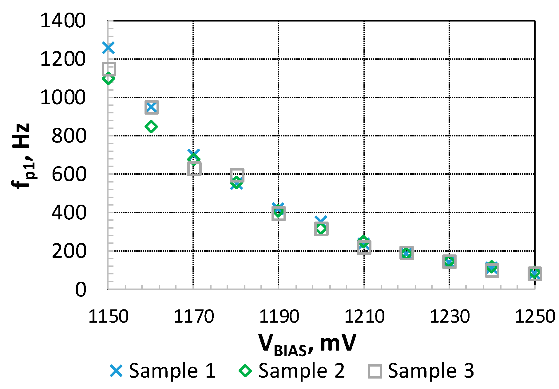
| VBIAS (V) | R2 (GΩ) | fp1 (Hz) | fp2 (kHz) | Av_max (dB) | Noise (μV2RMS) | THDmax (dB) |
|---|---|---|---|---|---|---|
| 1.15 | 1.47 | 973 | 5.5 | 54.8 | 2.04 | −15.7 |
| 1.2 | 6.42 | 248 | 4.6 | 54.7 | 2.22 | −29.9 |
| 1.25 | 28.5 | 55 | 4.6 | 54.5 | 2.46 | −52.7 |
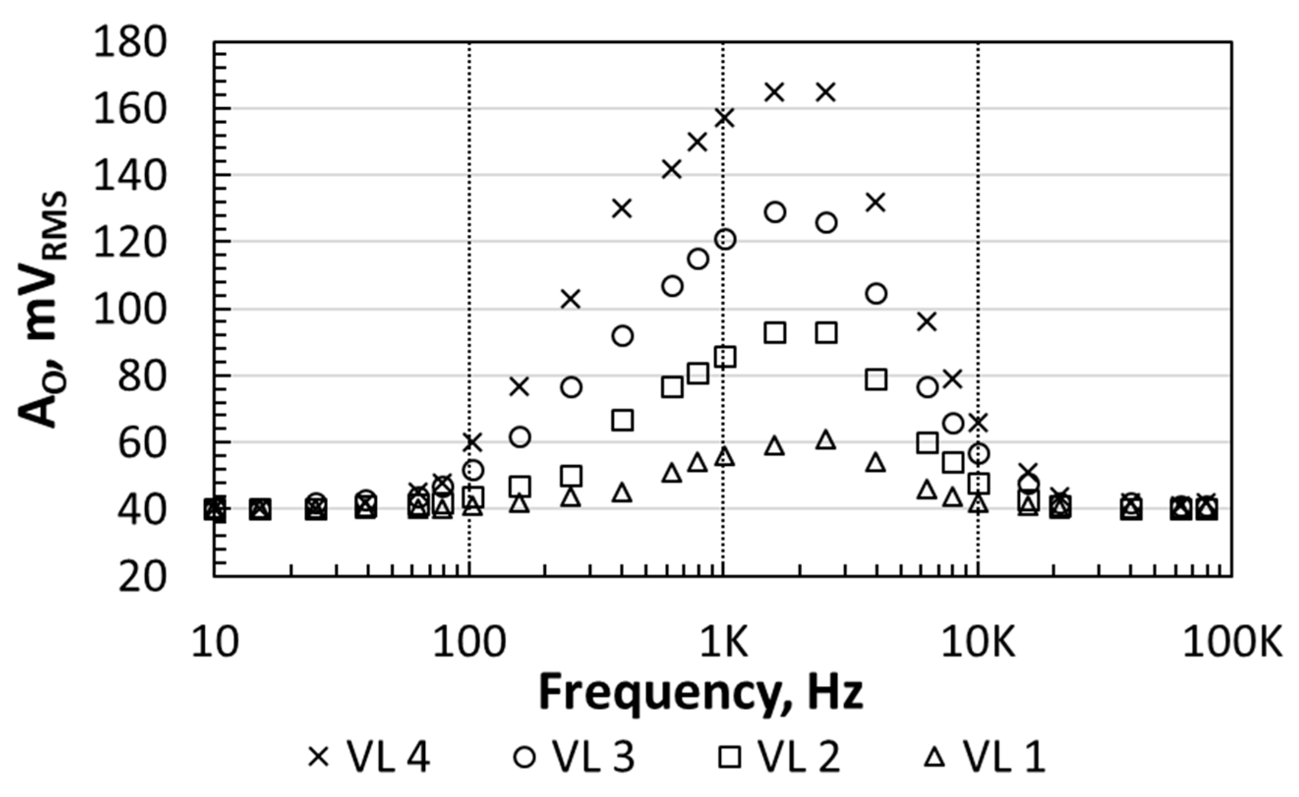
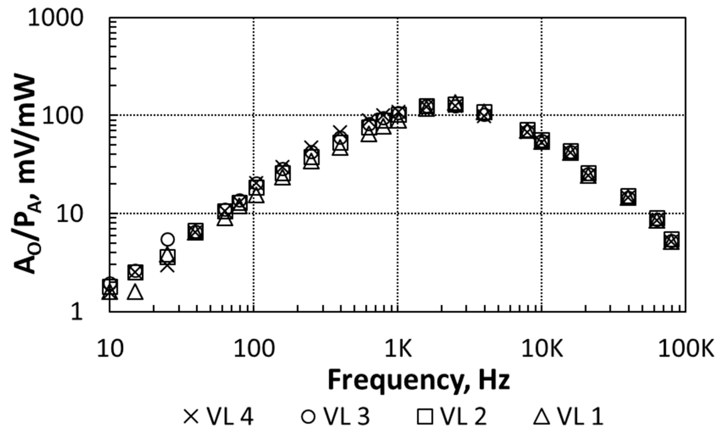
| VL | VDCh (V) | A (mVRMS) | PA (mW) |
|---|---|---|---|
| 1 | 1.67 | 7.8 | 0.44 |
| 2 | 1.67 | 15 | 0.84 |
| 3 | 1.67 | 23 | 1.29 |
| 4 | 1.67 | 31 | 1.75 |
| VBIAS (V) | fp1 (Hz) | fp2 (kHz) | Av_max (dB) |
|---|---|---|---|
| 1.15 | 1258 | 5.1 | 54.1 |
| 1.2 | 350 | 3.9 | 54.9 |
| 1.25 | 79 | 3.9 | 54.6 |
Publisher’s Note: MDPI stays neutral with regard to jurisdictional claims in published maps and institutional affiliations. |
© 2021 by the authors. Licensee MDPI, Basel, Switzerland. This article is an open access article distributed under the terms and conditions of the Creative Commons Attribution (CC BY) license (http://creativecommons.org/licenses/by/4.0/).
Share and Cite
Altet, J.; Barajas, E.; Mateo, D.; Billong, A.; Aragones, X.; Perpiñà, X.; Reverter, F. BPF-Based Thermal Sensor Circuit for On-Chip Testing of RF Circuits. Sensors 2021, 21, 805. https://doi.org/10.3390/s21030805
Altet J, Barajas E, Mateo D, Billong A, Aragones X, Perpiñà X, Reverter F. BPF-Based Thermal Sensor Circuit for On-Chip Testing of RF Circuits. Sensors. 2021; 21(3):805. https://doi.org/10.3390/s21030805
Chicago/Turabian StyleAltet, Josep, Enrique Barajas, Diego Mateo, Alexandre Billong, Xavier Aragones, Xavier Perpiñà, and Ferran Reverter. 2021. "BPF-Based Thermal Sensor Circuit for On-Chip Testing of RF Circuits" Sensors 21, no. 3: 805. https://doi.org/10.3390/s21030805