
MoS2 Based Photodetectors: A Review


Abstract
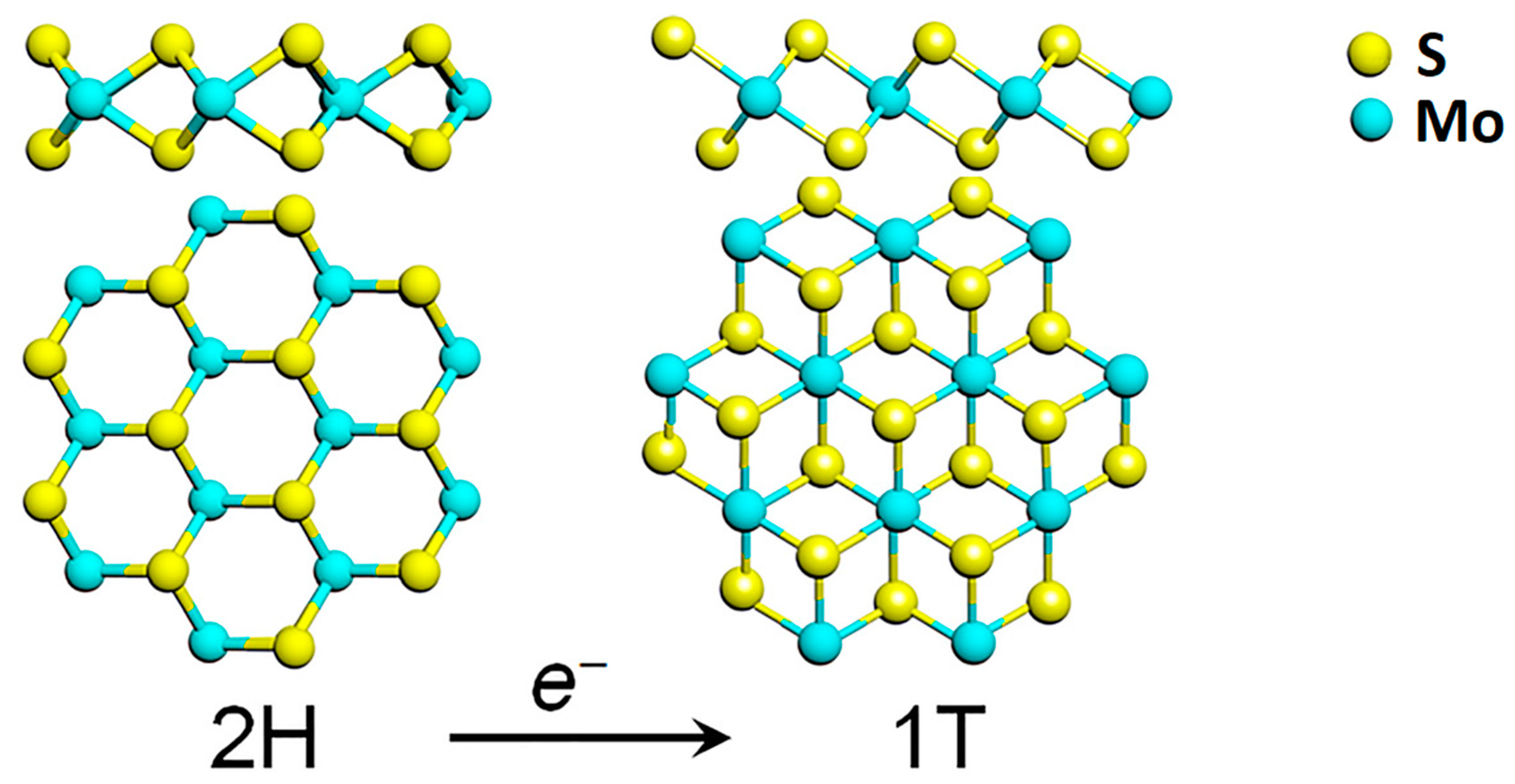
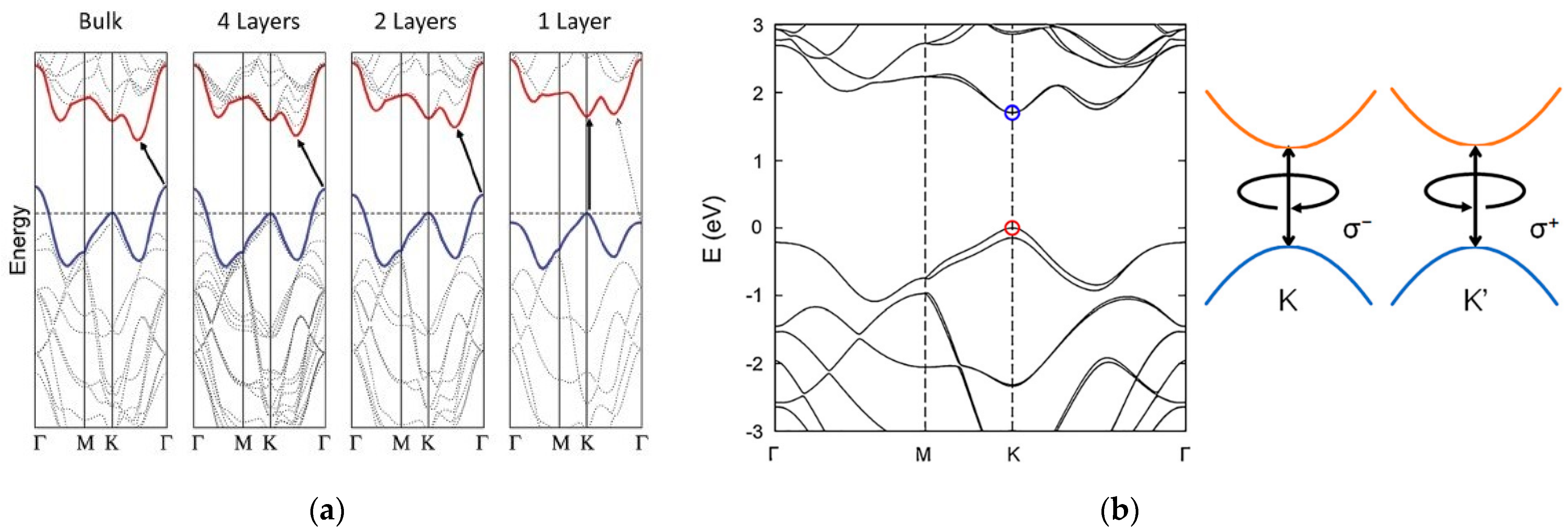
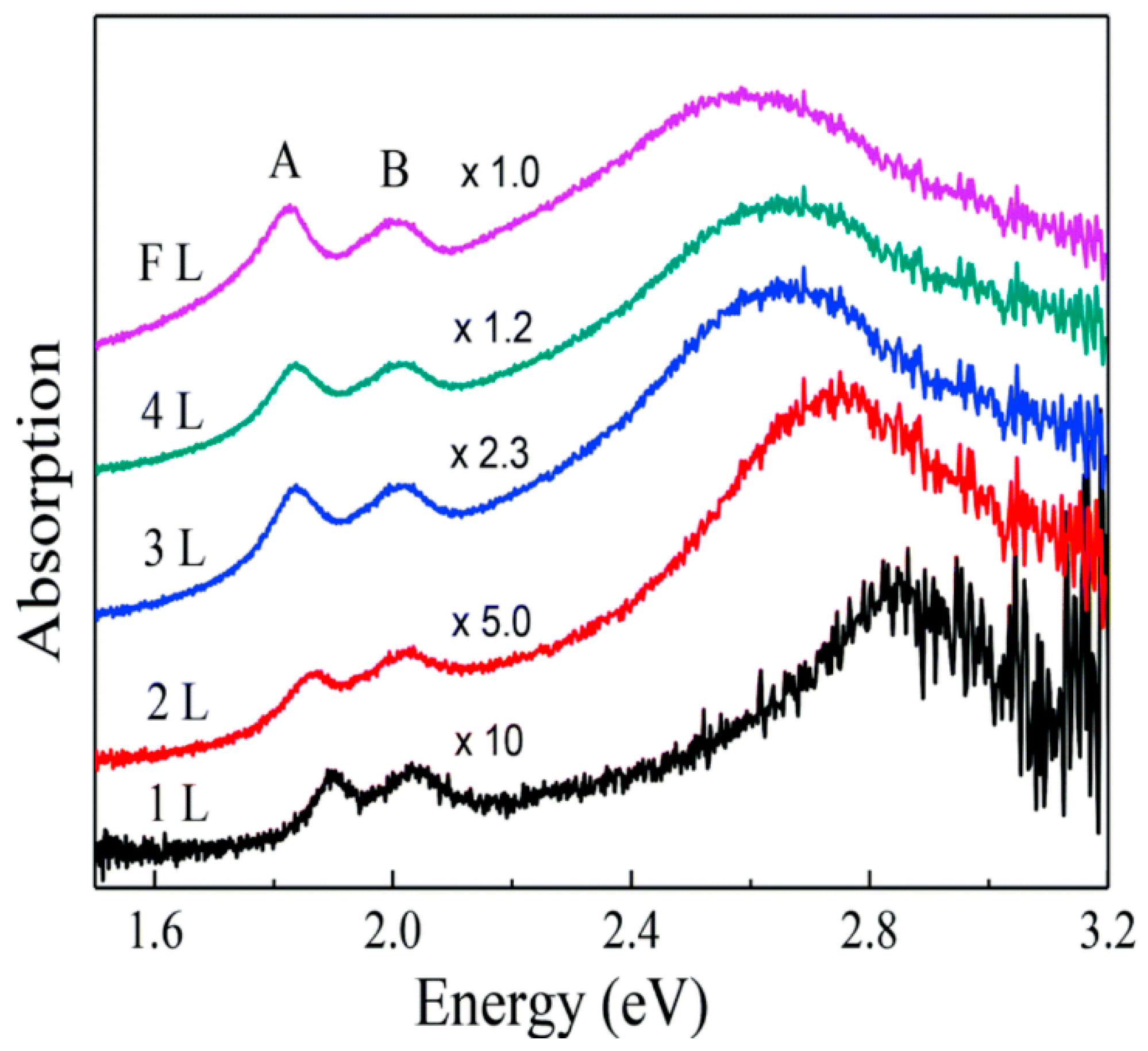
:1. Introduction
2. MoS2 Photodetectors
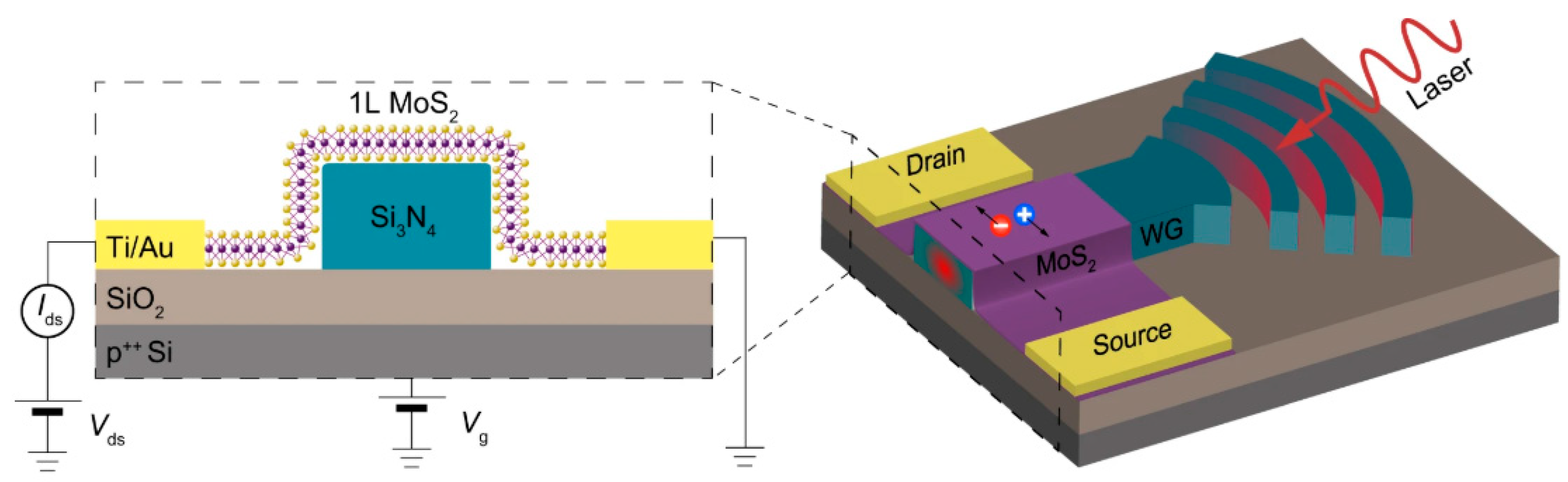
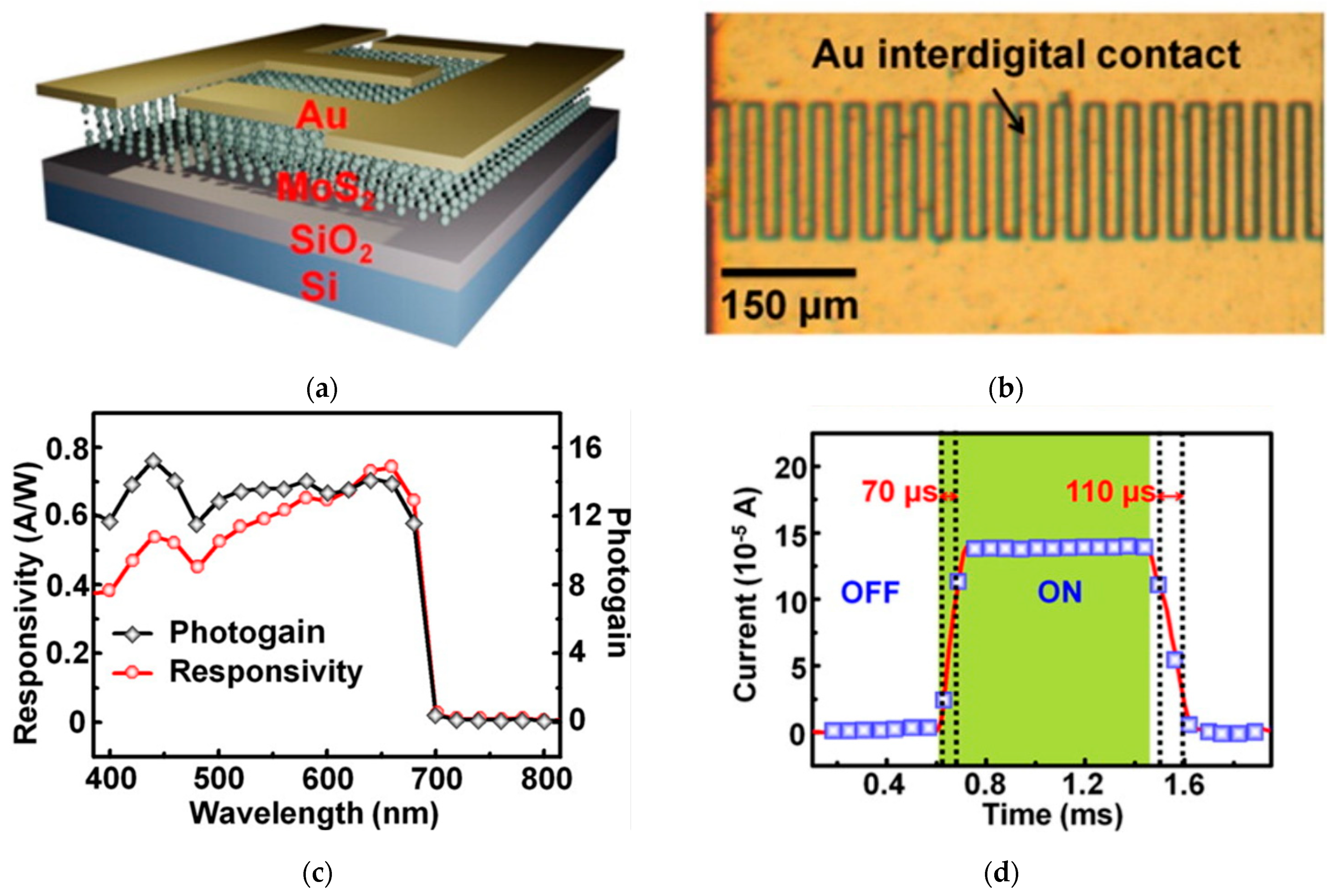
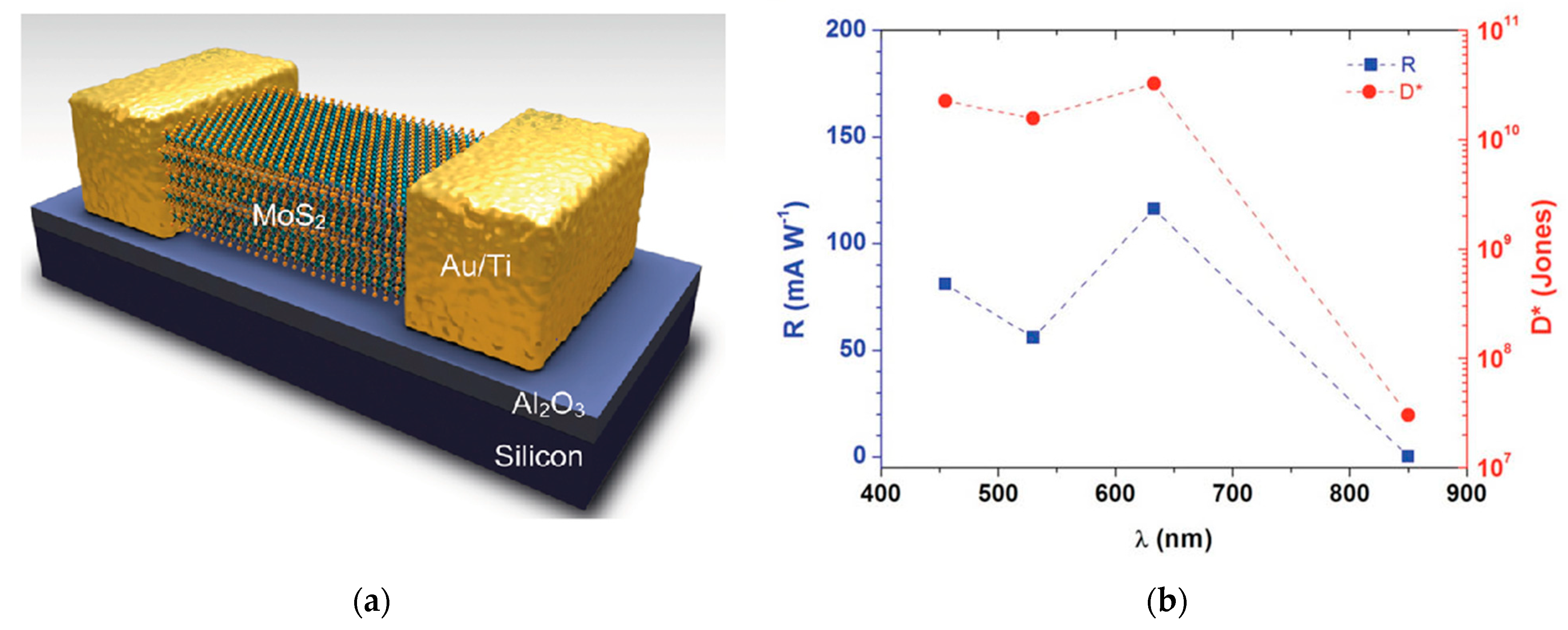
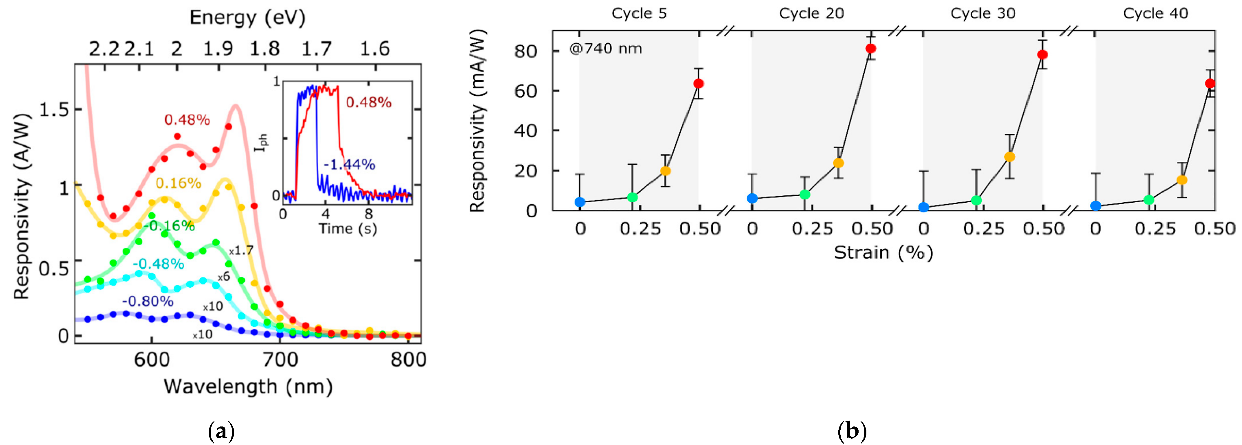
2.1. Neat MoS2 Photodetectors
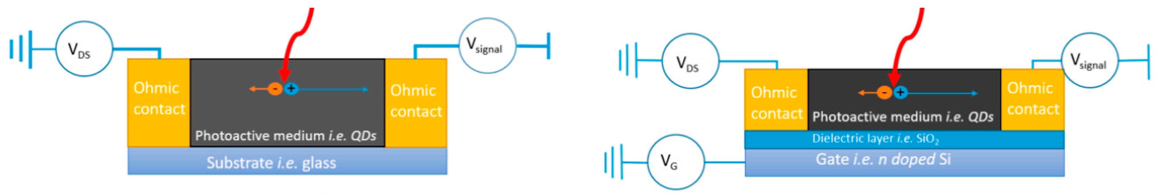
2.2. MoS2 + QDs Based Photodetectors
2.3. MoS2 + Graphene Based Photodetectors
2.4. MoS2 + TMDs Based Photodetectors
2.5. MoS2 + Perovskites Based Photodetectors
3. Conclusions
Author Contributions
Funding
Institutional Review Board Statement
Informed Consent Statement
Data Availability Statement
Conflicts of Interest
References
- Huo, N.; Konstantatos, G. Recent progress and future prospects of 2D-based photodetectors. Adv. Mater. 2018, 30, 1801164. [Google Scholar] [CrossRef]
- Mueller, T.; Xia, F.; Avouris, P. Graphene photodetectors for high-speed optical communications. Nat. Photonics 2010, 4, 297–301. [Google Scholar] [CrossRef] [Green Version]
- Radisavljevic, B.; Radenovic, A.; Brivio, J.; Giacometti, V.; Kis, A. Single-layer MoS2 transistors. Nat. Nanotechnol. 2011, 6, 147–150. [Google Scholar] [CrossRef] [PubMed]
- Mak, K.F.; Lee, C.; Hone, J.; Shan, J.; Heinz, T.F. Atomically thin MoS2: A new direct-gap semiconductor. Phys. Rev. Lett. 2010, 105, 136805. [Google Scholar] [CrossRef] [PubMed] [Green Version]
- Bernardi, M.; Palummo, M.; Grossman, J.C. Extraordinary sunlight absorption and one nanometer thick photovoltaics using two-dimensional monolayer materials. Nano Lett. 2013, 13, 3664–3670. [Google Scholar] [CrossRef]
- Li, X.; Tao, L.; Chen, Z.; Fang, H.; Li, X.; Wang, X.; Xu, J.B.; Zhu, H. Graphene and related two-dimensional materials: Structure-property relationships for electronics and optoelectronics. Appl. Phys. Rev. 2017, 4, 021306. [Google Scholar] [CrossRef]
- Sandoval, S.J.; Yang, D.; Frindt, R.F.; Irwin, J.C. Raman study and lattice dynamics of single molecular layers of MoS2. Phys. Rev. B 1991, 44, 3955–3962. [Google Scholar] [CrossRef] [PubMed]
- Voiry, D.; Goswami, A.; Kappera, R.; Silva, C.; Kaplan, D.; Fujita, T.; Chen, M.; Asefa, T.; Chhowalla, M. Covalent functionalization of monolayered transition metal dichalcogenides by phase engineering. Nat. Chem. 2015, 7, 45–49. [Google Scholar] [CrossRef]
- Kang, Y.; Najmaei, S.; Liu, Z.; Bao, Y.; Wang, Y.; Zhu, X.; Halas, N.J.; Nordlander, P.; Ajayan, P.M.; Lou, J.; et al. Plasmonic Hot Electron Induced Structural Phase Transition in a MoS2 Monolayer. Adv. Mater. 2014, 26, 6467–6471. [Google Scholar] [CrossRef] [PubMed]
- Katagiri, Y.; Nakamura, T.; Ishii, A.; Ohata, C.; Hasegawa, M.; Katsumoto, S.; Cusati, T.; Fortunelli, A.; Iannaccone, G.; Fiori, G.; et al. Gate-tunable atomically thin lateral MoS2 Schottky junction patterned by electron beam. Nano Lett. 2016, 16, 3788–3794. [Google Scholar] [CrossRef]
- Li, T.; Galli, G. Electronic Properties of MoS2 Nanoparticles. J. Phys. Chem. C 2007, 111, 16192–16196. [Google Scholar] [CrossRef]
- Lebègue, S.; Eriksson, O. Electronic structure of two-dimensional crystals from ab initio theory. Phys. Rev. B Condens. Matter Mater. Phys. 2009, 79. [Google Scholar] [CrossRef] [Green Version]
- Cheiwchanchamnangij, T.; Lambrecht, W.R.L. Quasiparticle band structure calculation of monolayer, bilayer, and bulk MoS2. Phys. Rev. B Condens. Matter Mater. Phys. 2012, 85. [Google Scholar] [CrossRef] [Green Version]
- Kam, K.K.; Parkinson, B.A. Detailed photocurrent spectroscopy of the semiconducting group VIB transition metal dichalcogenides. J. Phys. Chem. 1982, 86, 463–467. [Google Scholar] [CrossRef]
- Splendiani, A.; Sun, L.; Zhang, Y.; Li, T.; Kim, J.; Chim, C.Y.; Galli, G.; Wang, F. Emerging photoluminescence in monolayer MoS2. Nano Lett. 2010, 10, 1271–1275. [Google Scholar] [CrossRef] [PubMed]
- Xiao, D.; Liu, G.B.; Feng, W.; Xu, X.; Yao, W. Coupled spin and valley physics in monolayers of MoS2 and other group-VI dichalcogenides. Phys. Rev. Lett. 2012, 108. [Google Scholar] [CrossRef] [Green Version]
- Zeng, H.; Dai, J.; Yao, W.; Xiao, D.; Cui, X. Valley polarization in MoS2 monolayers by optical pumping. Nat. Nanotechnol. 2012, 7. [Google Scholar] [CrossRef]
- Schaibley, J.R.; Yu, H.; Clark, G.; Rivera, P.; Ross, J.S.; Seyler, K.L.; Yao, W.; Xu, X. Valleytronics in 2D materials. Nat. Rev. Mater. 2016, 1, 16055. [Google Scholar] [CrossRef]
- Liu, Y.; Gao, Y.; Zhang, S.; He, J.; Yu, J.; Liu, Z. Valleytronics in transition metal dichalcogenides materials. Nano Res. 2019, 12. [Google Scholar] [CrossRef]
- Dhakal, K.P.; Duong, D.L.; Lee, J.; Nam, H.; Kim, M.; Kan, M.; Lee, Y.H.; Kim, J. Confocal absorption spectral imaging of MoS2: Optical transitions depending on the atomic thickness of intrinsic and chemically doped MoS2. Nanoscale 2014, 6. [Google Scholar] [CrossRef] [Green Version]
- Kwak, J.Y. Absorption coefficient estimation of thin MoS2 film using attenuation of silicon substrate Raman signal. Results Phys. 2019, 13, 102202. [Google Scholar] [CrossRef]
- Novoselov, K.S.; Jiang, D.; Schedin, F.; Booth, T.J.; Khotkevich, V.V.; Morozov, S.V.; Geim, A.K. Two-dimensional atomic crystals. Proc. Natl. Acad. Sci. USA 2005, 102. [Google Scholar] [CrossRef] [Green Version]
- Choi, W.; Cho, M.Y.; Konar, A.; Lee, J.H.; Cha, G.B.; Hong, S.C.; Kim, S.; Kim, J.; Jena, D.; Joo, J.; et al. High-detectivity multilayer MoS2 phototransistors with spectral response from ultraviolet to infrared. Adv. Mater. 2012, 24, 5832–5836. [Google Scholar] [CrossRef]
- Lopez-Sanchez, O.; Lembke, D.; Kayci, M.; Radenovic, A.; Kis, A. Ultrasensitive photodetectors based on monolayer MoS2. Nat. Nanotechnol. 2013, 8, 497–501. [Google Scholar] [CrossRef] [PubMed]
- He, J.; Yang, Y.; He, Y.; Ge, C.; Zhao, Y.; Gao, L.; Tang, J. Low Noise and Fast Photoresponse of Few-Layered MoS2 Passivated by MA3Bi2Br9. ACS Photonics 2018, 5, 1877–1884. [Google Scholar] [CrossRef]
- Gant, P.; Huang, P.; de Lara, D.P.; Guo, D.; Frisenda, R.; Castellanos-Gomez, A. A strain tunable single-layer MoS2 photodetector. Mater. Today 2019, 27, 8–13. [Google Scholar] [CrossRef]
- Gonzalez Marin, J.F.; Unuchek, D.; Watanabe, K.; Taniguchi, T.; Kis, A. MoS2 photodetectors integrated with photonic circuits. NPJ 2D Mater. Appl. 2019, 3. [Google Scholar] [CrossRef] [Green Version]
- Wang, H.; Wang, X.; Chen, Y.; Zhang, S.; Jiang, W.; Zhang, X.; Qin, J.; Wang, J.; Li, X.; Pan, Y.; et al. Extremely Low Dark Current MoS2 Photodetector via 2D Halide Perovskite as the Electron Reservoir. Adv. Opt. Mater. 2020, 8, 1901402. [Google Scholar] [CrossRef]
- Klots, A.R.; Newaz, A.K.M.; Wang, B.; Prasai, D.; Krzyzanowska, H.; Lin, J.; Caudel, D.; Ghimire, N.J.; Yan, J.; Ivanov, B.L.; et al. Probing excitonic states in suspended two-dimensional semiconductors by photocurrent spectroscopy. Sci. Rep. 2014, 4, 6608. [Google Scholar] [CrossRef] [PubMed]
- Wi, S.; Chen, M.; Nam, H.; Liu, A.C.; Meyhofer, E.; Liang, X. High blue-near ultraviolet photodiode response of vertically stacked graphene-MoS2-metal heterostructures. Appl. Phys. Lett. 2014, 104, 232103. [Google Scholar] [CrossRef]
- Li, X.; Wu, J.; Mao, N.; Zhang, J.; Lei, Z.; Liu, Z.; Xu, H. A self-powered graphene-MoS2 hybrid phototransistor with fast response rate and high on-off ratio. Carbon N. Y. 2015, 92, 126–132. [Google Scholar] [CrossRef]
- Kufer, D.; Nikitskiy, I.; Lasanta, T.; Navickaite, G.; Koppens, F.H.L.; Konstantatos, G. Hybrid 2D-0D MoS2-PbS quantum dot photodetectors. Adv. Mater. 2015, 27, 176–180. [Google Scholar] [CrossRef]
- Long, M.; Liu, E.; Wang, P.; Gao, A.; Xia, H.; Luo, W.; Wang, B.; Zeng, J.; Fu, Y.; Xu, K.; et al. Broadband Photovoltaic Detectors Based on an Atomically Thin Heterostructure. Nano Lett. 2016, 16, 2254–2259. [Google Scholar] [CrossRef] [PubMed]
- Ra, H.S.; Kwak, D.H.; Lee, J.S. A hybrid MoS2 nanosheet-CdSe nanocrystal phototransistor with a fast photoresponse. Nanoscale 2016, 8, 17223–17230. [Google Scholar] [CrossRef]
- Huo, N.; Gupta, S.; Konstantatos, G. MoS2–HgTe Quantum Dot Hybrid Photodetectors beyond 2 µm. Adv. Mater. 2017, 29, 1606576. [Google Scholar] [CrossRef] [PubMed]
- Chen, Y.; Wang, X.; Wu, G.; Wang, Z.; Fang, H.; Lin, T.; Sun, S.; Shen, H.; Hu, W.; Wang, J.; et al. High-Performance Photovoltaic Detector Based on MoTe2/MoS2 Van der Waals Heterostructure. Small 2018, 14, 1703293. [Google Scholar] [CrossRef] [PubMed]
- Magda, G.Z.; Petõ, J.; Dobrik, G.; Hwang, C.; Biró, L.P.; Tapasztó, L. Exfoliation of large-area transition metal chalcogenide single layers. Sci. Rep. 2015, 5, 14714. [Google Scholar] [CrossRef] [Green Version]
- Sun, J.; Li, X.; Guo, W.; Zhao, M.; Fan, X.; Dong, Y.; Xu, C.; Deng, J.; Fu, Y. Synthesis methods of two-dimensional MoS2: A brief review. Crystals 2017, 7, 198. [Google Scholar] [CrossRef]
- Ahn, C.; Lee, J.; Kim, H.U.; Bark, H.; Jeon, M.; Ryu, G.H.; Lee, Z.; Yeom, G.Y.; Kim, K.; Jung, J.; et al. Low-Temperature Synthesis of Large-Scale Molybdenum Disulfide Thin Films Directly on a Plastic Substrate Using Plasma-Enhanced Chemical Vapor Deposition. Adv. Mater. 2015, 27, 5223–5229. [Google Scholar] [CrossRef]
- Zhou, X.; Xu, B.; Lin, Z.; Shu, D.; Ma, L. Hydrothermal synthesis of flower-like MoS2nanospheres for electrochemical supercapacitors. J. Nanosci. Nanotechnol. 2014, 14, 7250–7254. [Google Scholar] [CrossRef] [PubMed]
- Feng, X.; Tang, Q.; Zhou, J.; Fang, J.; Ding, P.; Sun, L.; Shi, L. Novel mixed-solvothermal synthesis of MoS2 nanosheets with controllable morphologies. Cryst. Res. Technol. 2013, 48, 363–368. [Google Scholar] [CrossRef]
- Nardi, M.V.; Timpel, M.; Ligorio, G.; Zorn Morales, N.; Chiappini, A.; Toccoli, T.; Verucchi, R.; Ceccato, R.; Pasquali, L.; List-Kratochvil, E.J.W.; et al. Versatile and Scalable Strategy to Grow Sol-Gel Derived 2H-MoS2 Thin Films with Superior Electronic Properties: A Memristive Case. ACS Appl. Mater. Interfaces 2018, 10, 34392–34400. [Google Scholar] [CrossRef] [PubMed]
- Suh, J.; Park, T.E.; Lin, D.Y.; Fu, D.; Park, J.; Jung, H.J.; Chen, Y.; Ko, C.; Jang, C.; Sun, Y.; et al. Doping against the native propensity of MoS2: Degenerate hole doping by cation substitution. Nano Lett. 2014, 14. [Google Scholar] [CrossRef]
- Li, M.; Yao, J.; Wu, X.; Zhang, S.; Xing, B.; Niu, X.; Yan, X.; Yu, Y.; Liu, Y.; Wang, Y. P-type Doping in Large-Area Monolayer MoS2 by Chemical Vapor Deposition. ACS Appl. Mater. Interfaces 2020, 12, 6276–6282. [Google Scholar] [CrossRef] [PubMed]
- Kim, E.; Ko, C.; Kim, K.; Chen, Y.; Suh, J.; Ryu, S.G.; Wu, K.; Meng, X.; Suslu, A.; Tongay, S.; et al. Site Selective Doping of Ultrathin Metal Dichalcogenides by Laser-Assisted Reaction. Adv. Mater. 2016, 28, 341–346. [Google Scholar] [CrossRef]
- Zhang, K.; Feng, S.; Wang, J.; Azcatl, A.; Lu, N.; Addou, R.; Wang, N.; Zhou, C.; Lerach, J.; Bojan, V.; et al. Erratum: Manganese Doping of Monolayer MoS2: The Substrate Is Critical (Nano Letters 2015, 15:10 (6586-6591) 10.1021/acs.nanolett.5b02315). Nano Lett. 2016, 16, 2125. [Google Scholar] [CrossRef]
- Chen, M.; Nam, H.; Wi, S.; Ji, L.; Ren, X.; Bian, L.; Lu, S.; Liang, X. Stable few-layer MoS2 rectifying diodes formed by plasma-assisted doping. Appl. Phys. Lett. 2013, 103, 142110. [Google Scholar] [CrossRef]
- Mouri, S.; Miyauchi, Y.; Matsuda, K. Tunable photoluminescence of monolayer MoS2 via chemical doping. Nano Lett. 2013, 13, 5944–5948. [Google Scholar] [CrossRef] [PubMed] [Green Version]
- Nakotte, T.; Luo, H.; Pietryga, J. PbE (E = S, Se) colloidal quantum dot-layered 2D material hybrid photodetectors. Nanomaterials 2020, 10, 172. [Google Scholar] [CrossRef] [Green Version]
- Tsai, D.S.; Liu, K.K.; Lien, D.H.; Tsai, M.L.; Kang, C.F.; Lin, C.A.; Li, L.J.; He, J.H. Few-layer MoS2 with high broadband photogain and fast optical switching for use in harsh environments. ACS Nano 2013, 7, 3905–3911. [Google Scholar] [CrossRef] [PubMed]
- AYore, E.; Smithe, K.K.H.; Jha, S.; Ray, K.; Pop, E.; Newaz, A.K.M. Large array fabrication of high performance monolayer MoS2 photodetectors. Appl. Phys. Lett. 2017, 111, 043110. [Google Scholar] [CrossRef] [Green Version]
- Sahatiya, P.; Jones, S.S.; Badhulika, S. 2D MoS2–carbon quantum dot hybrid based large area, flexible UV–vis–NIR photodetector on paper substrate. Appl. Mater. Today 2018, 10, 106–114. [Google Scholar] [CrossRef]
- Gomathi, P.T.; Sahatiya, P.; Badhulika, S. Large-Area, Flexible Broadband Photodetector Based on ZnS–MoS2 Hybrid on Paper Substrate. Adv. Funct. Mater. 2017, 27, 1701611. [Google Scholar] [CrossRef]
- Kang, M.A.; Kim, S.; Jeon, I.S.; Lim, Y.R.; Park, C.Y.; Song, W.; Lee, S.S.; Lim, J.; An, K.S.; Myung, S. Highly efficient and flexible photodetector based on MoS2-ZnO heterostructures. RSC Adv. 2019, 9, 19707–19711. [Google Scholar] [CrossRef] [Green Version]
- Bolotin, K.I.; Sikes, K.J.; Jiang, Z.; Klima, M.; Fudenberg, G.; Hone, J.; Kim, P.; Stormer, H.L. Ultrahigh electron mobility in suspended graphene. Solid State Commun. 2008, 146, 351–355. [Google Scholar] [CrossRef] [Green Version]
- Mak, K.F.; Shan, J. Photonics and optoelectronics of 2D semiconductor transition metal dichalcogenides. Nat. Photonics 2016, 10, 216–226. [Google Scholar] [CrossRef]
- Tan, H.; Xu, W.; Sheng, Y.; Lau, C.S.; Fan, Y.; Chen, Q.; Tweedie, M.; Wang, X.; Zhou, Y.; Warner, J.H. Lateral Graphene-Contacted Vertically Stacked WS2/MoS2 Hybrid Photodetectors with Large Gain. Adv. Mater. 2017, 29, 1702917. [Google Scholar] [CrossRef]
- Zheng, K.; Luo, L.B.; Zhang, T.F.; Liu, Y.H.; Yu, Y.Q.; Lu, R.; Qiu, H.L.; Li, Z.J.; Huang, J.C.A. Optoelectronic characteristics of a near infrared light photodetector based on a topological insulator Sb2Te3 film. J. Mater. Chem. C 2015, 3, 9154–9160. [Google Scholar] [CrossRef]
- Furchi, M.M.; Polyushkin, D.K.; Pospischil, A.; Mueller, T. Mechanisms of photoconductivity in atomically thin MoS2. Nano Lett. 2014, 14, 6165–6170. [Google Scholar] [CrossRef] [Green Version]
- Pak, J.; Min, M.; Cho, K.; Lien, D.H.; Ahn, G.H.; Jang, J.; Yoo, D.; Chung, S.; Javey, A.; Lee, T. Improved photoswitching response times of MoS2 field-effect transistors by stacking p -type copper phthalocyanine layer. Appl. Phys. Lett. 2016, 109, 183502. [Google Scholar] [CrossRef] [Green Version]
- Tang, J.; Kemp, K.W.; Hoogland, S.; Jeong, K.S.; Liu, H.; Levina, L.; Furukawa, M.; Wang, X.; Debnath, R.; Cha, D.; et al. Colloidal-quantum-dot photovoltaics using atomic-ligand passivation. Nat. Mater. 2011, 10, 765–771. [Google Scholar] [CrossRef]
- Zhang, X.M.; Tseng, S.H.; Lu, M.Y. Large-area ultraviolet photodetectors based on p-type multilayer MoS2 enabled by plasma doping. Appl. Sci. 2019, 9, 1110. [Google Scholar] [CrossRef] [Green Version]
- Kumar, R.; Goel, N.; Raliya, R.; Biswas, P.; Kumar, M. High-performance photodetector based on hybrid of MoS2 and reduced graphene oxide. Nanotechnology 2018, 29, 404001. [Google Scholar] [CrossRef]
- Solanke, S.; Rathakanthiwar, S.; Kalra, A.; Rangarajan, M.; Raghavan, S.; Nath, D.N. Multi-layer MoS2/GaN UV-Visible photodetector with observation of MoS2band edge in spectral responsivity. arXiv 2018, arXiv:1803.11012. [Google Scholar]
- Kumar, R.; Sharma, A.; Kaur, M.; Husale, S. Pt-Nanostrip-Enabled Plasmonically Enhanced Broad Spectral Photodetection in Bilayer MoS2. Adv. Opt. Mater. 2017, 5, 1700009. [Google Scholar] [CrossRef]
- Zhou, X.; Zhou, N.; Li, C.; Song, H.; Zhang, Q.; Hu, X.; Gan, L.; Li, H.; Lü, J.; Luo, J.; et al. Vertical heterostructures based on SnSe2/MoS2 for high performance photodetectors. 2D Mater. 2017, 4, 025048. [Google Scholar] [CrossRef]
- Yu, W.J.; Liu, Y.; Zhou, H.; Yin, A.; Li, Z.; Huang, Y.; Duan, X. Highly efficient gate-tunable photocurrent generation in vertical heterostructures of layered materials. Nat. Nanotechnol. 2013, 8, 952–958. [Google Scholar] [CrossRef] [Green Version]
- Tsai, D.S.; Lien, D.H.; Tsai, M.L.; Su, S.H.; Chen, K.M.; Ke, J.J.; Yu, Y.C.; Li, L.J.; He, J.H. Trilayered MoS2 metal-Semiconductor-metal photodetectors: Photogain and radiation resistance. IEEE J. Sel. Top. Quantum Electron. 2014, 20, 3800206. [Google Scholar] [CrossRef]
- Zhang, W.; Chuu, C.P.; Huang, J.K.; Chen, C.H.; Tsai, M.L.; Chang, Y.H.; Liang, C.T.; Chen, Y.Z.; Chueh, Y.L.; He, J.H.; et al. Ultrahigh-Gain Photodetectors Based on Atomically Thin Graphene-MoS2 Heterostructures. Sci. Rep. 2015, 4, 3826. [Google Scholar] [CrossRef] [Green Version]
- Vabbina, P.; Choudhary, N.; Chowdhury, A.A.; Sinha, R.; Karabiyik, M.; Das, S.; Choi, W.; Pala, N. Highly Sensitive Wide Bandwidth Photodetector Based on Internal Photoemission in CVD Grown p-Type MoS2/Graphene Schottky Junction. ACS Appl. Mater. Interfaces 2015, 7, 15206–15213. [Google Scholar] [CrossRef]
- Ye, K.; Liu, L.; Liu, Y.; Nie, A.; Zhai, K.; Xiang, J.; Wang, B.; Wen, F.; Mu, C.; Zhao, Z.; et al. Lateral Bilayer MoS2–WS2 Heterostructure Photodetectors with High Responsivity and Detectivity. Adv. Opt. Mater. 2019, 7, 1900815. [Google Scholar] [CrossRef]
- Shin, G.H.; Park, J.; Lee, K.J.; Lee, G.B.; Jeon, H.B.; Choi, Y.K.; Yu, K.; Choi, S.Y. Si-MoS2 vertical heterojunction for a photodetector with high responsivity and low noise equivalent power. ACS Appl. Mater. Interfaces 2019, 11, 7626–7634. [Google Scholar] [CrossRef]
- Wang, L.; Jie, J.; Shao, Z.; Zhang, Q.; Zhang, X.; Wang, Y.; Sun, Z.; Lee, S.T. MoS2/Si heterojunction with vertically standing layered structure for ultrafast, high-detectivity, self-driven visible-near infrared photodetectors. Adv. Funct. Mater. 2015, 25, 2910–2919. [Google Scholar] [CrossRef]
- Zhang, Y.; Yu, Y.; Mi, L.; Wang, H.; Zhu, Z.; Wu, Q.; Zhang, Y.; Jiang, Y. In Situ Fabrication of Vertical Multilayered MoS2/Si Homotype Heterojunction for High-Speed Visible-Near-Infrared Photodetectors. Small 2016, 12, 1062–1071. [Google Scholar] [CrossRef] [PubMed]
- Ye, L.; Li, H.; Chen, Z.; Xu, J. Near-Infrared Photodetector Based on MoS2/Black Phosphorus Heterojunction. ACS Photonics 2016, 3, 692–699. [Google Scholar] [CrossRef]


| Photoactive Material | Technology | MoS2 Layers | Wavelength (nm) | Responsivity (A/W) | Response Time (s) | Detectivity (Jones) | Dark Current (A) | Ref. | |
| MoS2 | MoS2 | phototransistor | 1L | 647 | 1000 | 13 | [27] | ||
| MoS2 | MSM photodiode | FL | 532 | 0.57 | tr 7 × 10⁻⁵ td 11 × 10−5 | 1010 | [50] | ||
| MoS2 | MSM photodiode | 1L | ≈400 | 10−3 | 0.5 × 10⁻³ | <10−14 | [51] | ||
| MoS2 | phototransistor | 1L | 561 | 880 | 9 | 2 × 10⁻¹² | [24] | ||
| MoS2 | phototransistor | 1L | 640 | 50 | 10−3 | [29] | |||
| MoS2 | phototransistor | ML | 633 | 0.12 | 1010–1011 | 10−11 | [23] | ||
| MoS2 | photodiode | FL | 365 | 9.3 | tr 3.7 × 10⁻² td 3.9 × 10⁻² | [62] | |||
| MoS2 | MSM photodiode | 3L | 532 | 1.04 | tr 4 × 10⁻⁵ td 5 × 10⁻⁵ | [68] | |||
| MoS2 + QDs/NPs | MoS2 + CQD | photoconductor | FL | 365 | 8.4 × 10⁻³ | 0.57 | ≈10−6 | [52] | |
| MoS2 + ZnS | photoconductor | 3L | 554 | 1.79 × 10⁻⁵ | 11 | [53] | |||
| 365 | 9.50 × 10⁻⁶ | 22 | [53] | ||||||
| 780 | 4.52 × 10⁻⁶ | 31 | [53] | ||||||
| MoS2 + CdSe | phototransistor | 2L | 405 | 2.50 × 10⁵ | 0.06 | 1.24 × 10¹⁴ | [34] | ||
| MoS2 + PbS | phototransistor | FL | 980 | 105 | 0.35 | 7 × 10¹⁴ | 2.6 × 10⁻⁷ | [32] | |
| MoS2 + HgTe | phototransistor | FL | 635 | 106 | 10−11 | [35] | |||
| 2000 | 105 | 1012 | [35] | ||||||
| MoS2 + ZnO | phototransistor | TF | 254 | 2.7 | 55 | [54] | |||
| MoS2 Heterostructures | MoS2 + Gr | phototransistor | FL | 632.8 | 3 | <1.3 × 10⁻⁴ | 9 × 10⁻¹⁰ | [31] | |
| MoS2 + MoTe2 | photodiode | FL | 637 | 4.60 × 10⁻² | 6 × 10⁻⁵ | 1.06 × 10⁸ | 3 × 10⁻¹² | [36] | |
| MoS2 + WS2 | phototransistor | 1L | 532 | 2340 | 4.1 × 10¹¹ | 10−6 | [57] | ||
| MoS2 + Gr + WSe2 | phototransistor | 1L/FL | 532 | 4250 | 5.4 × 10⁻⁵ | 1015 | [33] | ||
| 940 | 0.3 | 1011 | [33] | ||||||
| MoS2 + MA | photoconductor | 15L | 530 | 112 | 3 × 10⁻⁴ | 3.8 × 10¹² | 4 × 10⁻⁹ | [25] | |
| MoS2 + (PEA)2PbI4 | photoconductor | ML | 637 | 1.68 | tr 6 × 10⁻³ tr 4 × 10⁻³ | 1.06 × 10¹³ | 10−11 | [28] |
Publisher’s Note: MDPI stays neutral with regard to jurisdictional claims in published maps and institutional affiliations. |
© 2021 by the authors. Licensee MDPI, Basel, Switzerland. This article is an open access article distributed under the terms and conditions of the Creative Commons Attribution (CC BY) license (https://creativecommons.org/licenses/by/4.0/).
Share and Cite
Taffelli, A.; Dirè, S.; Quaranta, A.; Pancheri, L. MoS2 Based Photodetectors: A Review. Sensors 2021, 21, 2758. https://doi.org/10.3390/s21082758
Taffelli A, Dirè S, Quaranta A, Pancheri L. MoS2 Based Photodetectors: A Review. Sensors. 2021; 21(8):2758. https://doi.org/10.3390/s21082758
Chicago/Turabian StyleTaffelli, Alberto, Sandra Dirè, Alberto Quaranta, and Lucio Pancheri. 2021. "MoS2 Based Photodetectors: A Review" Sensors 21, no. 8: 2758. https://doi.org/10.3390/s21082758
APA StyleTaffelli, A., Dirè, S., Quaranta, A., & Pancheri, L. (2021). MoS2 Based Photodetectors: A Review. Sensors, 21(8), 2758. https://doi.org/10.3390/s21082758