
A Compact Measurement Setup for Material Characterization in W-Band Based on Dielectric Waveguides


Abstract
:1. Introduction
2. Fundamentals
2.1. Dielectric Waveguide
- Low weight;
- Flexibility due to their bendability;
- Easy fabrication, as well as length adaptation;
- Mechanically stable;
- Low material and manufacturing costs.
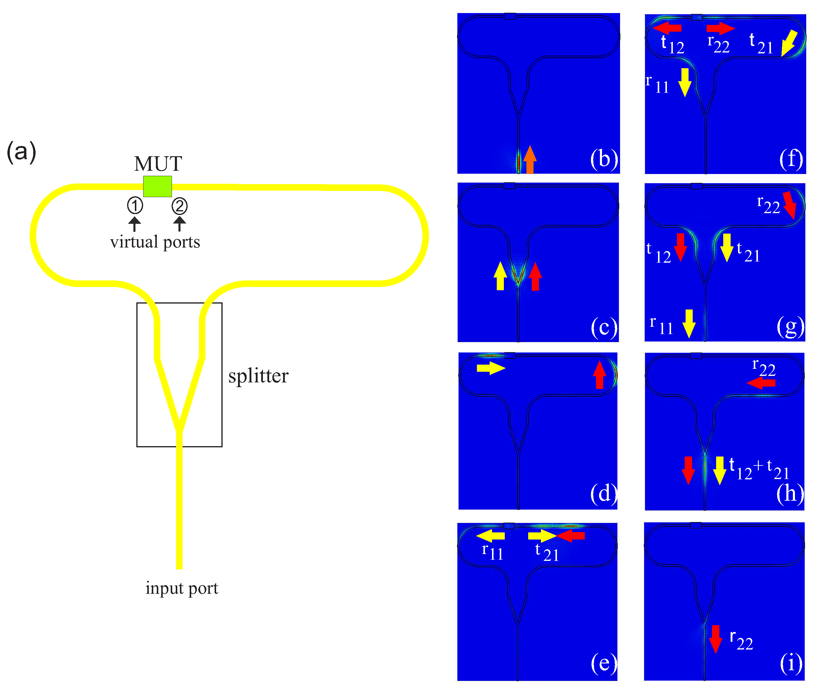
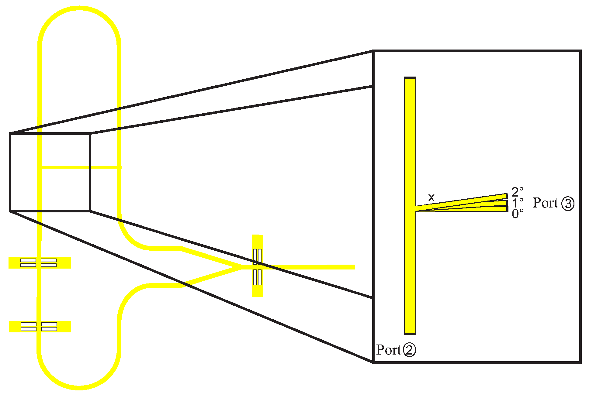
2.2. Concept
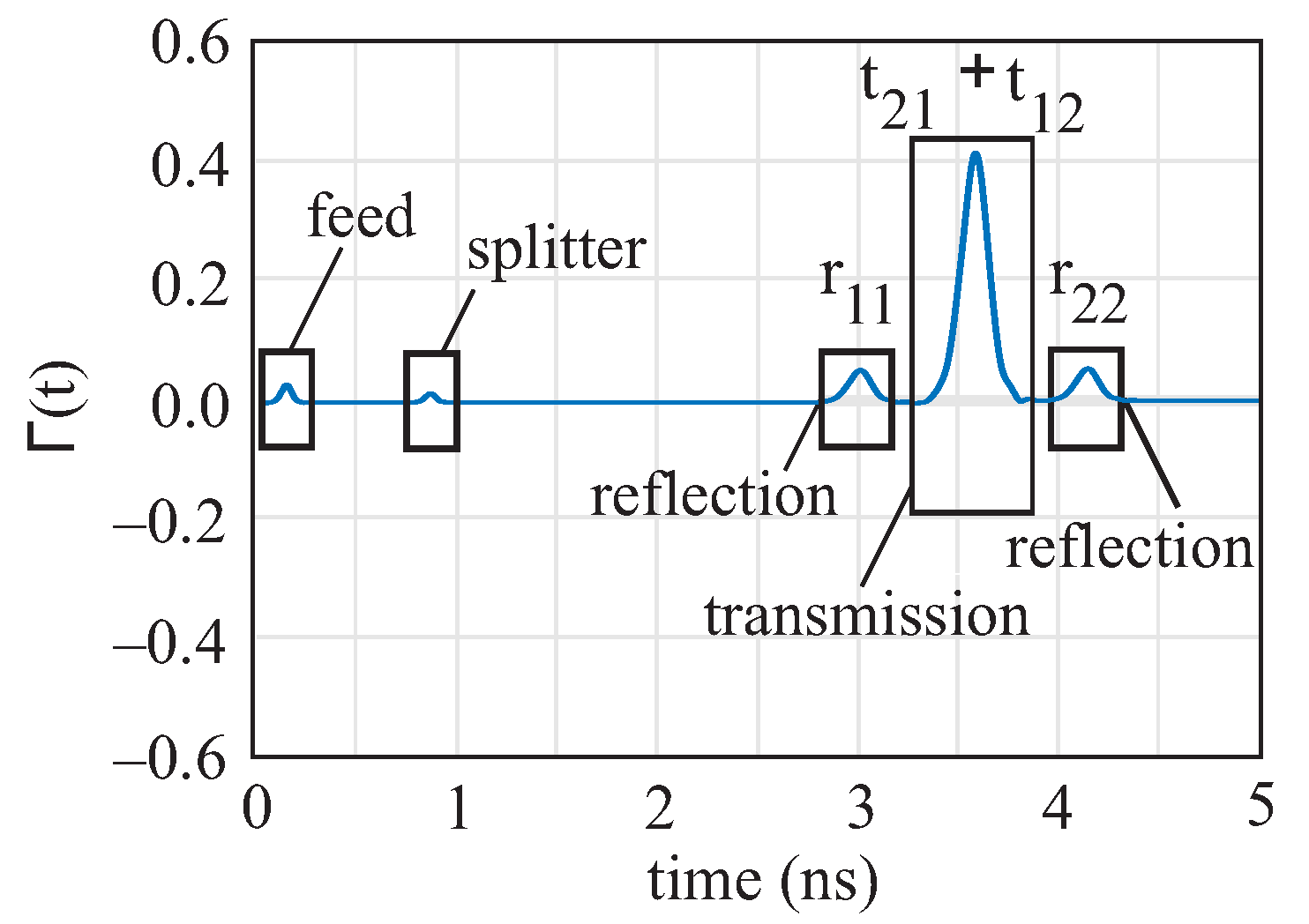
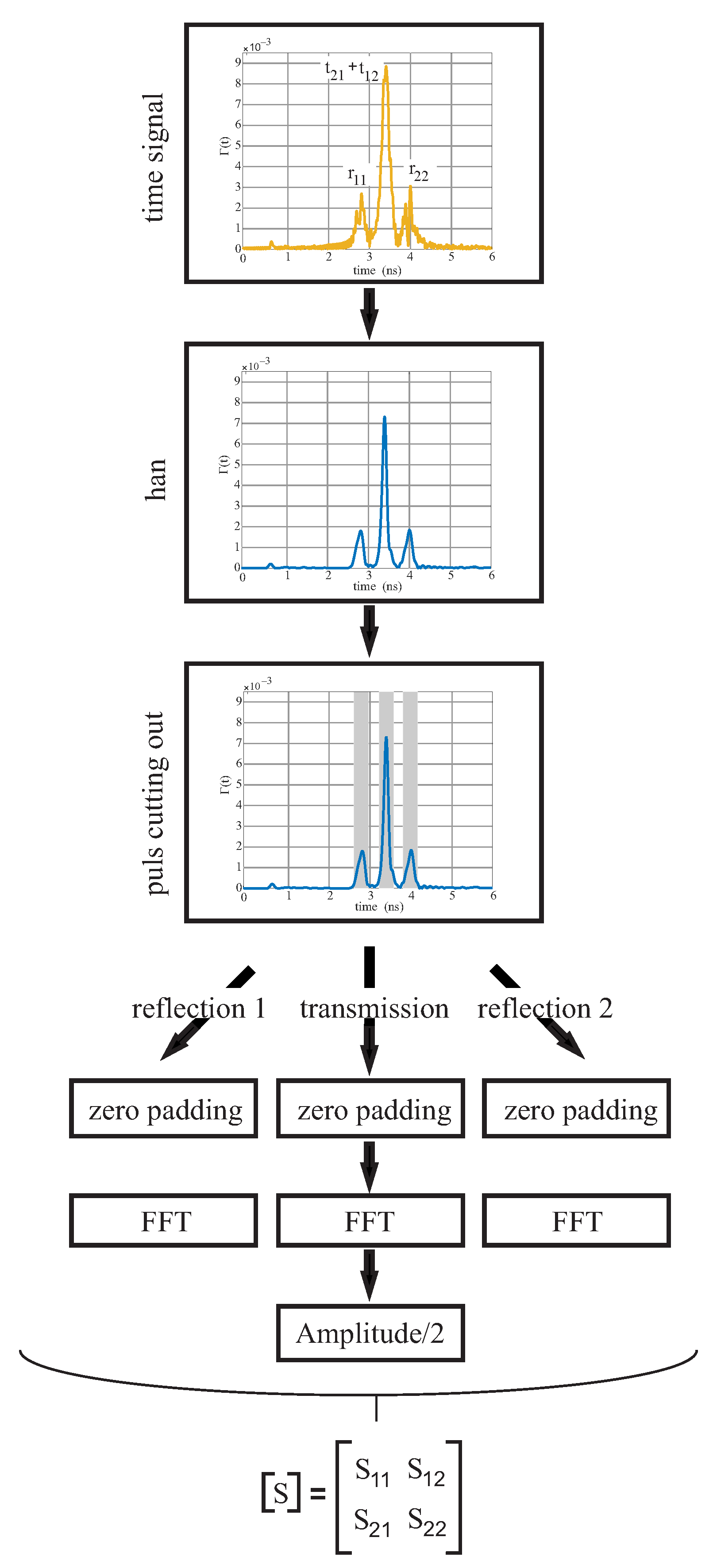
2.3. S-Parameters’ Extraction
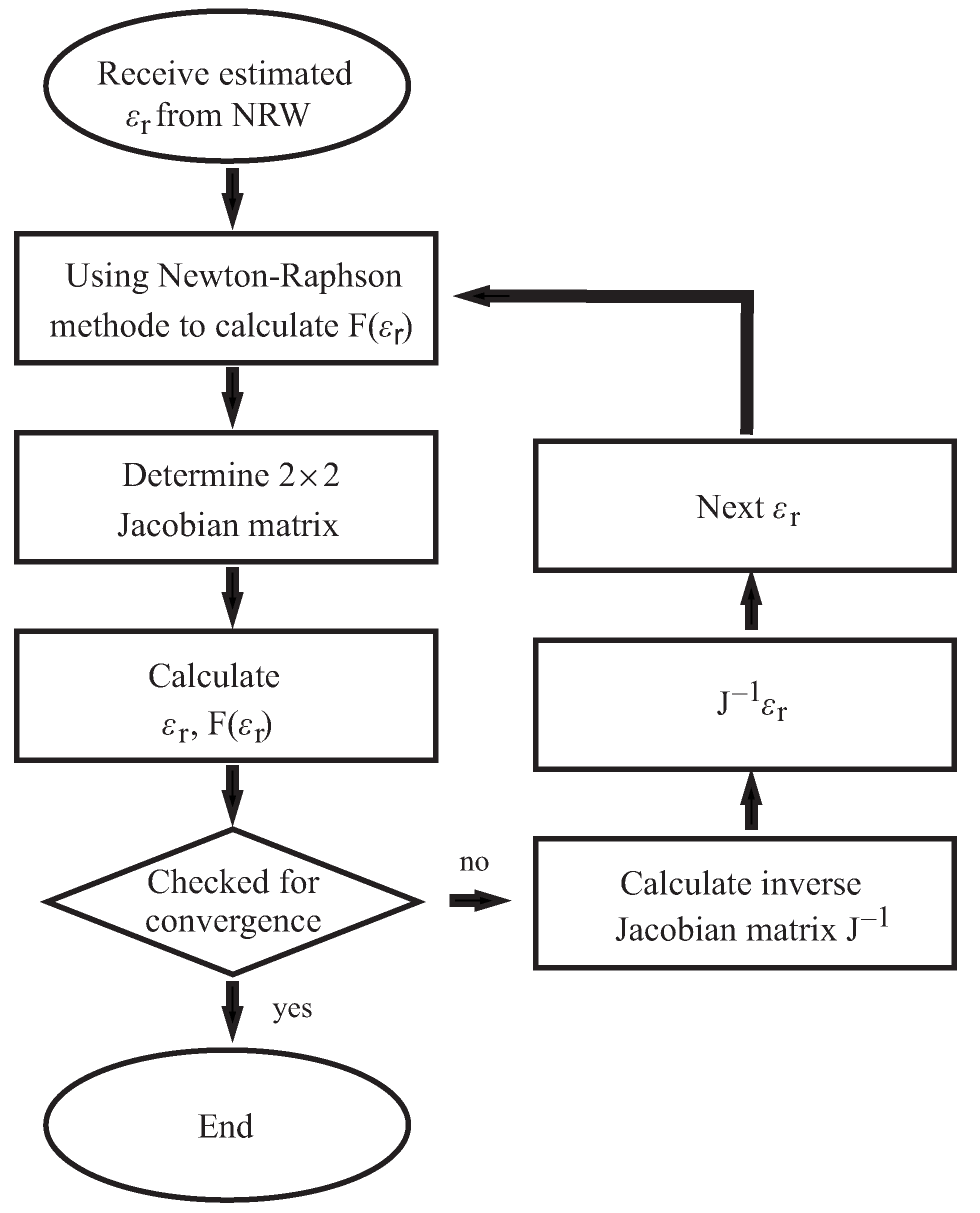
2.4. Algorithm
3. Simulation-Based Design
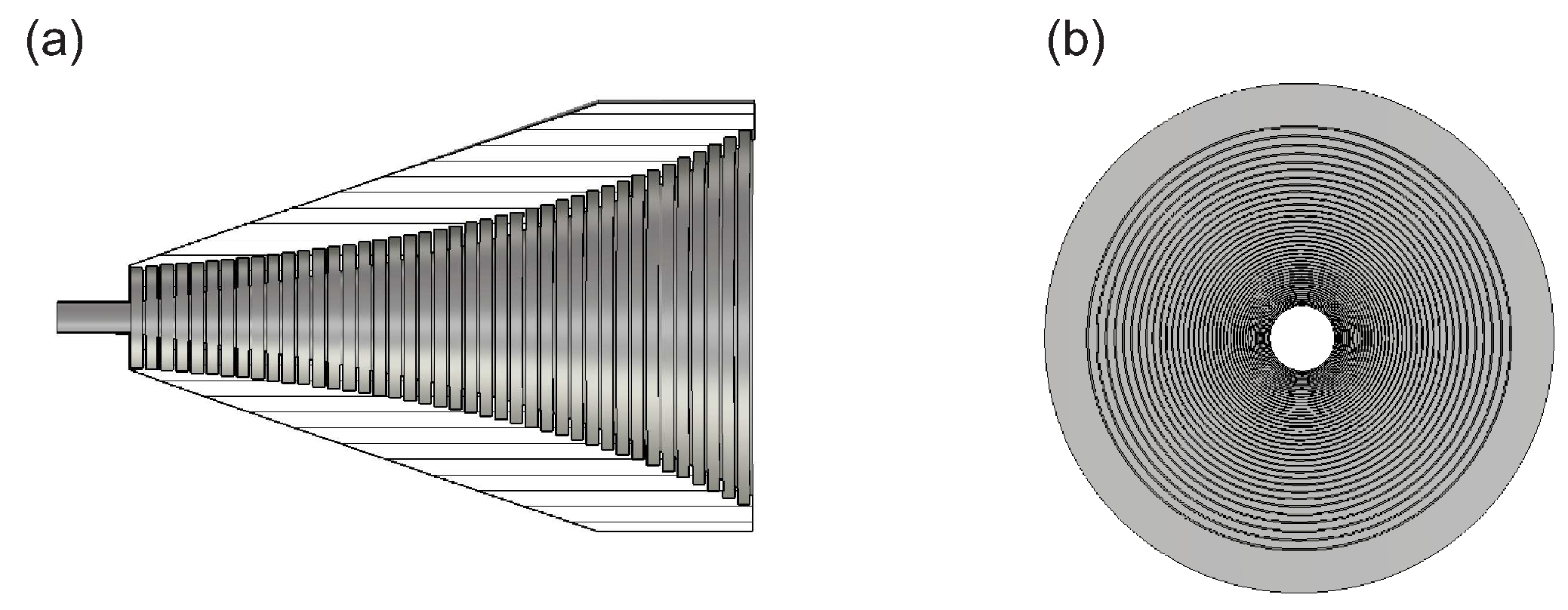
3.1. Support Structures
3.2. Mounting
3.3. Extension
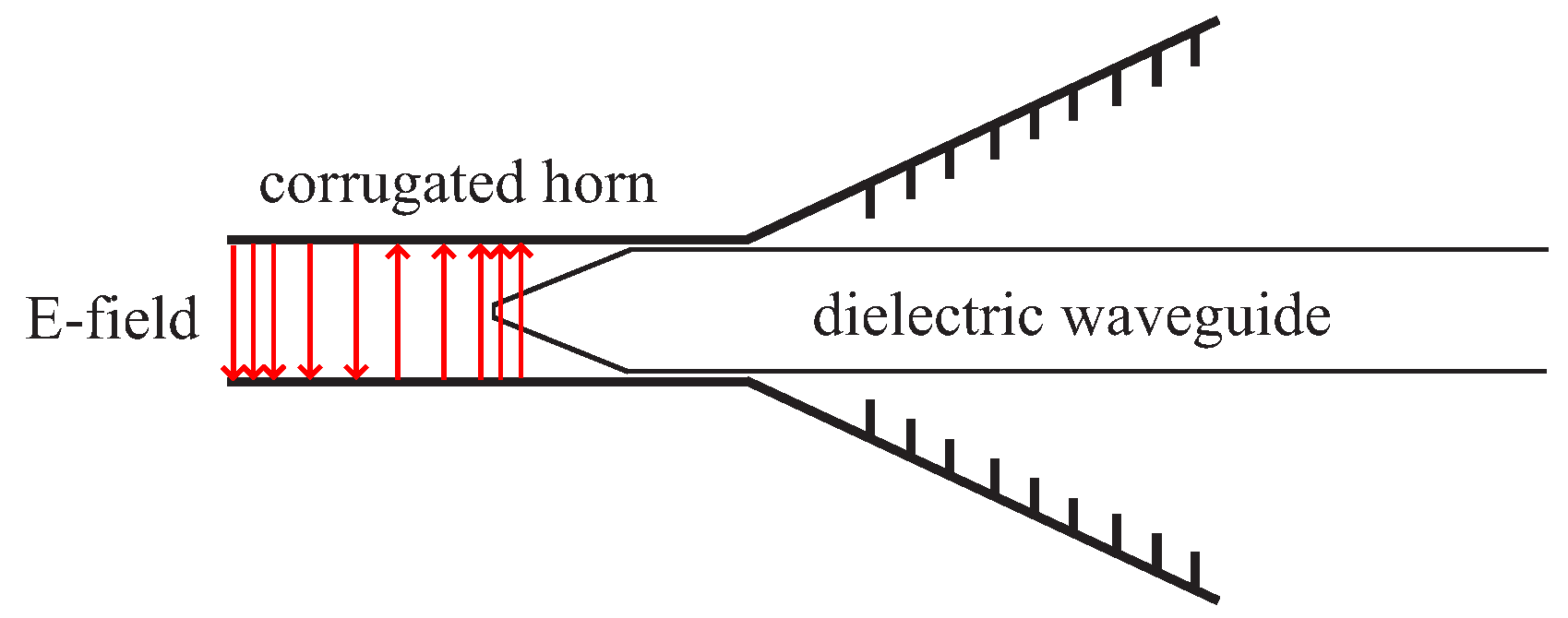
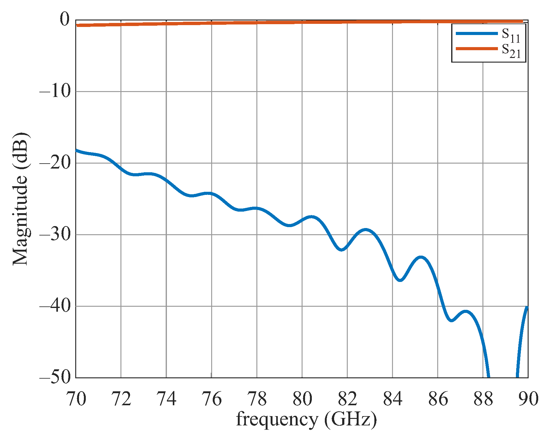
3.4. Transition
4. Processing and Calibration
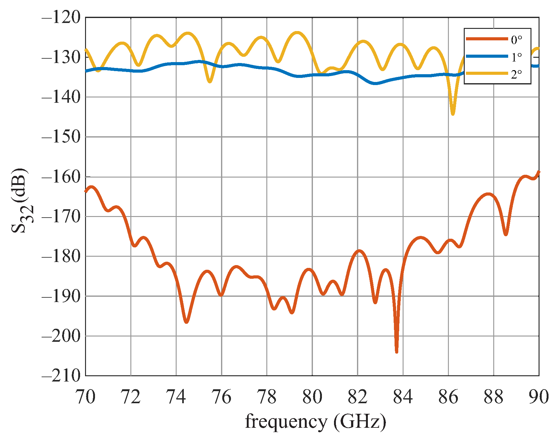
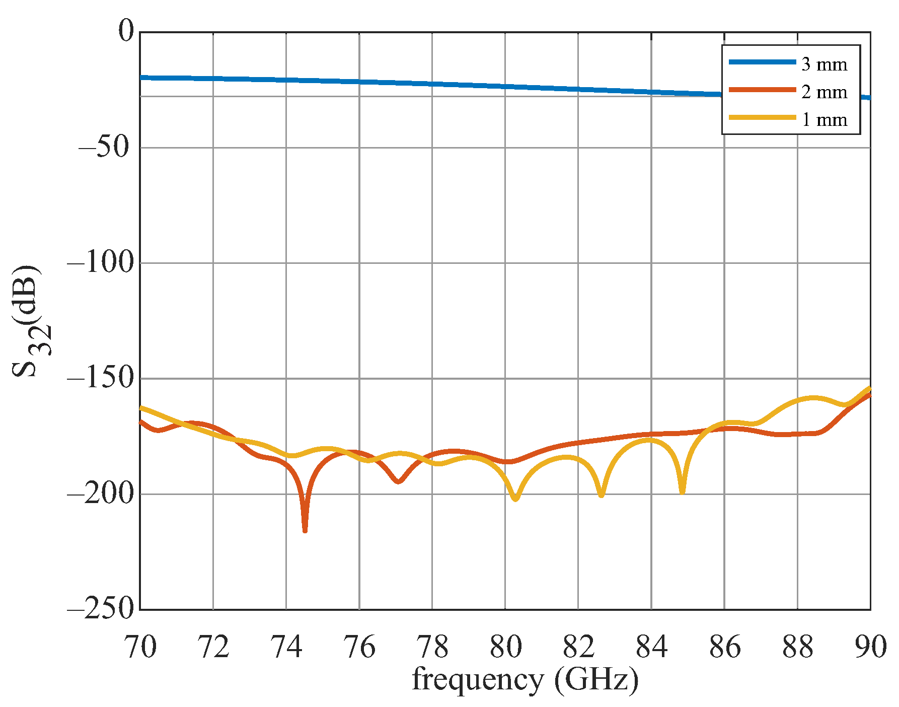
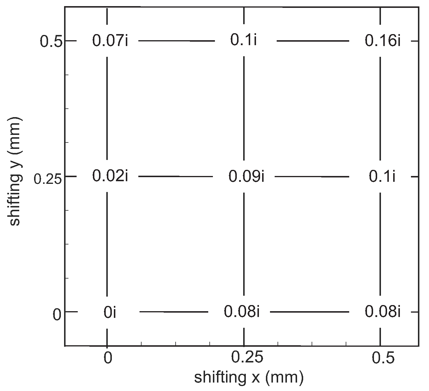
5. Tolerance and Accuracy
6. Measurements
6.1. Measurement Setup
6.2. Measurement Results
7. Conclusions
8. Discussion
Author Contributions
Funding
Conflicts of Interest
References
- Hoang, T.H.; Sharma, R.; Susanto, D.; Di Maso, M.; Kwong, E. Microwave assisted extraction of active pharmaceutical ingredient from solid dosage forms. J. Chromotography A 2007, 1156, 149–153. [Google Scholar] [CrossRef] [PubMed]
- Alves-Limaa, D.F.; Lia, X.; Coulsonb, B.; Neslingb, E.; Ludlama, G.A.H.; Degl’Innocentia, R.; Dawsona, R.; Peruffob, M.; Lin, H. Evaluation of water states in thin proton exchange membrane manufacturing using terahertz time-domain spectroscopy. J. Membr. Sci. 2022, 647, 120329. [Google Scholar] [CrossRef]
- Wee, F.H.; Soh, P.J.; Suhaizal, A.H.M.; Nornikman, H.; Ezanuddin, A.A.M. Free space measurement technique on dielectric properties of agricultural residues at microwave frequencies. In Proceedings of the 2009 SBMO/IEEE MTT-S International Microwave and Optoelectronics Conference (IMOC), Belem, Brazil, 3–6 November 2009. [Google Scholar]
- Nelson, S.O. Use of Electrical Properties for Grain-Moisture Measurement. J. Microw. Power 1977, 12, 67–72. [Google Scholar] [CrossRef]
- Kaatze, U. Techniques for measuring the microwave dielectric properties of materials. Metrologia 2010, 47, S91–S113. [Google Scholar] [CrossRef]
- Available online: https://mck.swissto12.ch/ (accessed on 1 July 2022).
- Barowski, J.; Jebramcik, J.; Alawneh, I.; Sheikh, F.; Kaiser, T.; Rolfes, I. A Compact Measurement Setup for In-Situ Material Characterization in the Lower THz Range. In Proceedings of the 2019 Second International Workshop on Mobile Terahertz Systems (IWMTS), Bad Neuenahr, Germany, 1–3 July 2019. [Google Scholar]
- Adler, R.B. Waves on inhomogeneous cylindrical structures. Proc. IRE 1952, 40, 339–348. [Google Scholar] [CrossRef]
- Gyorgy, E.M.; Weiss, M.T. Low loss dielectric waveguides. Microw. Theory Tech. 1954, 2, 38–47. [Google Scholar] [CrossRef]
- Šourková, H.; Špatenka, P. Plasma Activation of Polyethylene Powder. Polymers 2020, 12, 2099. [Google Scholar] [CrossRef] [PubMed]
- Baer, C. A reflectometer based sensor system for acquiring full S-parameter sets utilizing dielectric waveguides. In Proceedings of the 2019 IEEE Asia-Pacific Microwave Conference (APMC), Singapore, 10–13 December 2019; pp. 741–743. [Google Scholar]
- Nicolson, A.M.; Ross, G.F. Measurement of the Intrinsic Properties of Materials by Time-Domain Techniques. IEEE Trans. Instrum. Meas. 1970, 19, 377–382. [Google Scholar] [CrossRef] [Green Version]
- Weir, W.B. Automatic Measurement of Complex Dielectric Constant and Permeability. Proc. IEEE 1974, 62, 33–36. [Google Scholar] [CrossRef]
- Chen, L.F.; Ong, C.K.; Neo, C.P.; Varadan, V.V.; Varadan, V.K. Microwave Electronics Measurement and Materials Characterization; John Wiley & Sons Ltd.: Chichester, UK, 2004. [Google Scholar]
- Baker-Jarvis, J.; Vanzura, E.J.; Kissick, W.A. Improved Technique for Determining Complex Permittivity with the Transmission/Reflection Method. IEE Trans. Microw. Theory Tech. 1990, 38, 1096–1103. [Google Scholar] [CrossRef] [Green Version]
- Baer, C. On the applicability of TRL calibration for dielectric waveguide based 2-port-1-port systems. In Proceedings of the 2020 IEEE International Symposium on Antennas and Propagation and North American Radio Science Meeting, Montreal, QC, Canada, 5–10 July 2020; pp. 1625–1672. [Google Scholar]


| m | (2-port-1-port) | (MCK Swissto12) | % | % | |
|---|---|---|---|---|---|
| 4 | 2050 | 3.38 − 0.11i | 3.39 − 0.10i | −0.3 | 10 |
| 6 | 2060 | 3.91 − 0.13i | 3.98 − 0.12i | −1.76 | 8.3 |
| 8 | 4920 | 4.44 − 0.19i | 4.40 − 0.17i | 0.9 | 11.8 |
| 10 | 3989 | 5.00 − 0.26i | 5.01 − 0.23i | −0.20 | 8.0 |
| 12 | 4000 | 5.47 − 0.29i | 5.53 − 0.26i | −1.08 | 11.5 |
| 14 | 4000 | 5.97 − 0.32i | 5.99 − 0.29i | −0.33 | 10.3 |
| 15 | 3210 | 6.39 − 0.35i | 6.38 − 0.33i | 0.16 | 6.6 |
| 17 | 5110 | 6.46 − 0.36i | 6.45 − 0.32i | 0.15 | 12.5 |
| 18 | 5060 | 6.80 − 0.41i | 6.80 − 0.38i | −0.00 | 7.9 |
Publisher’s Note: MDPI stays neutral with regard to jurisdictional claims in published maps and institutional affiliations. |
© 2022 by the authors. Licensee MDPI, Basel, Switzerland. This article is an open access article distributed under the terms and conditions of the Creative Commons Attribution (CC BY) license (https://creativecommons.org/licenses/by/4.0/).
Share and Cite
Orend, K.; Baer, C.; Musch, T. A Compact Measurement Setup for Material Characterization in W-Band Based on Dielectric Waveguides. Sensors 2022, 22, 5972. https://doi.org/10.3390/s22165972
Orend K, Baer C, Musch T. A Compact Measurement Setup for Material Characterization in W-Band Based on Dielectric Waveguides. Sensors. 2022; 22(16):5972. https://doi.org/10.3390/s22165972
Chicago/Turabian StyleOrend, Kerstin, Christoph Baer, and Thomas Musch. 2022. "A Compact Measurement Setup for Material Characterization in W-Band Based on Dielectric Waveguides" Sensors 22, no. 16: 5972. https://doi.org/10.3390/s22165972