
Optimization of Au:CuO Thin Films by Plasma Surface Modification for High-Resolution LSPR Gas Sensing at Room Temperature

 ,
,  , ,
, ,  ,
,  , and
, and
Abstract
:1. Introduction
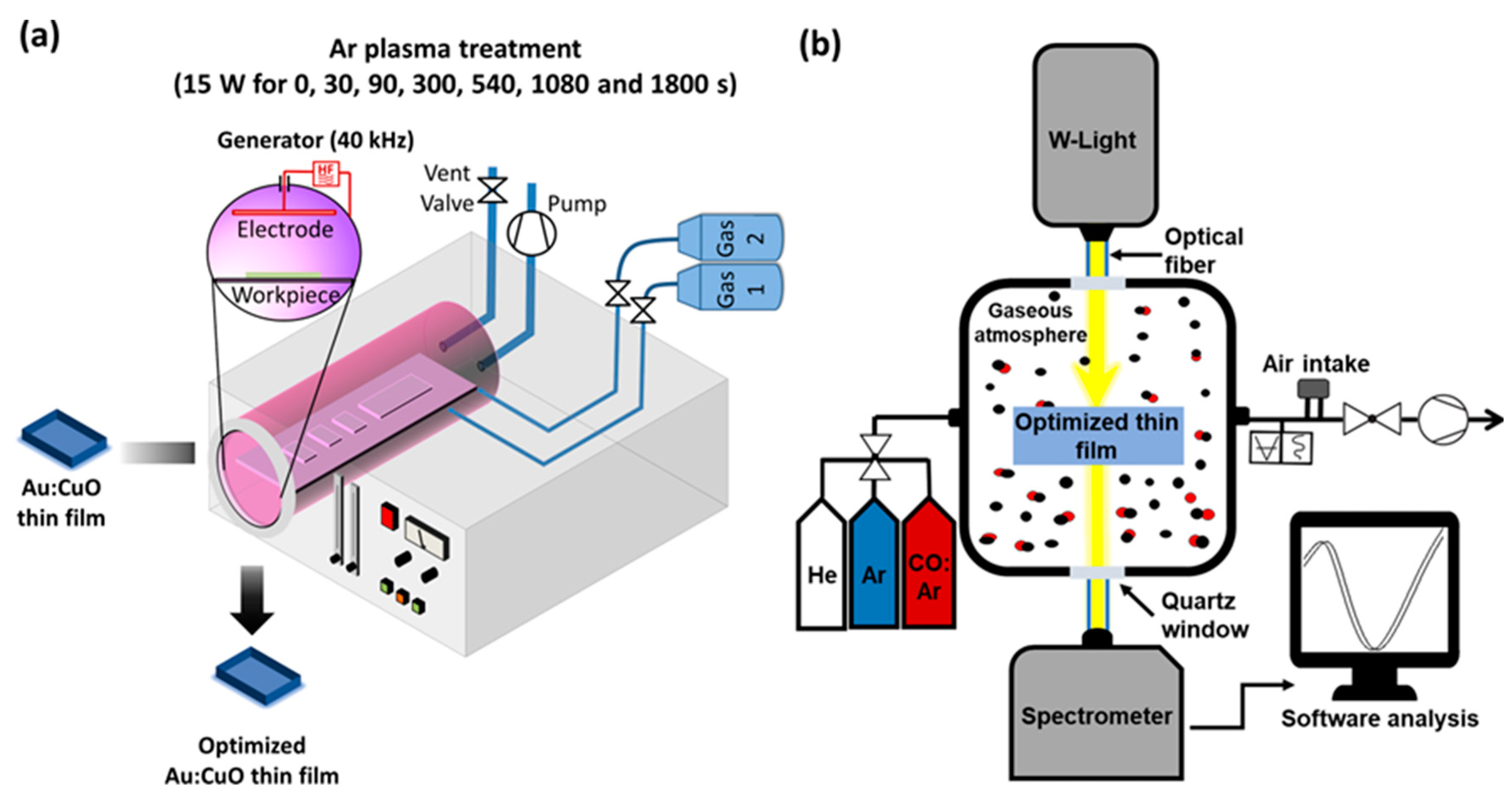
2. Materials and Methods
3. Results and Discussion
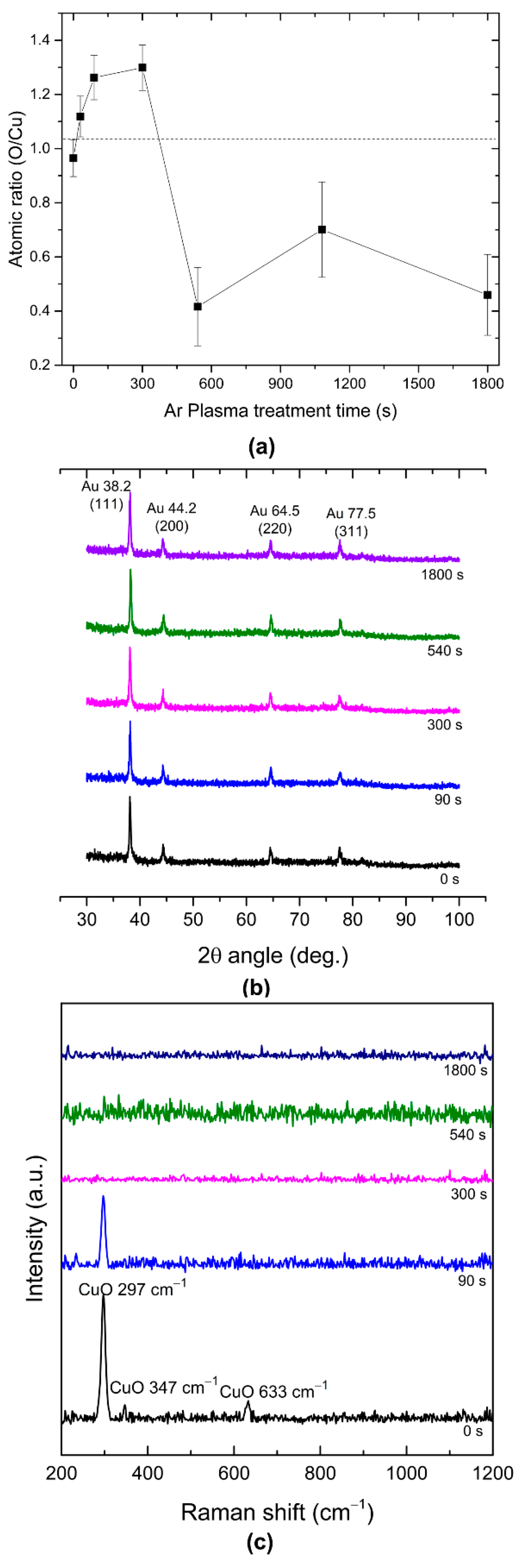
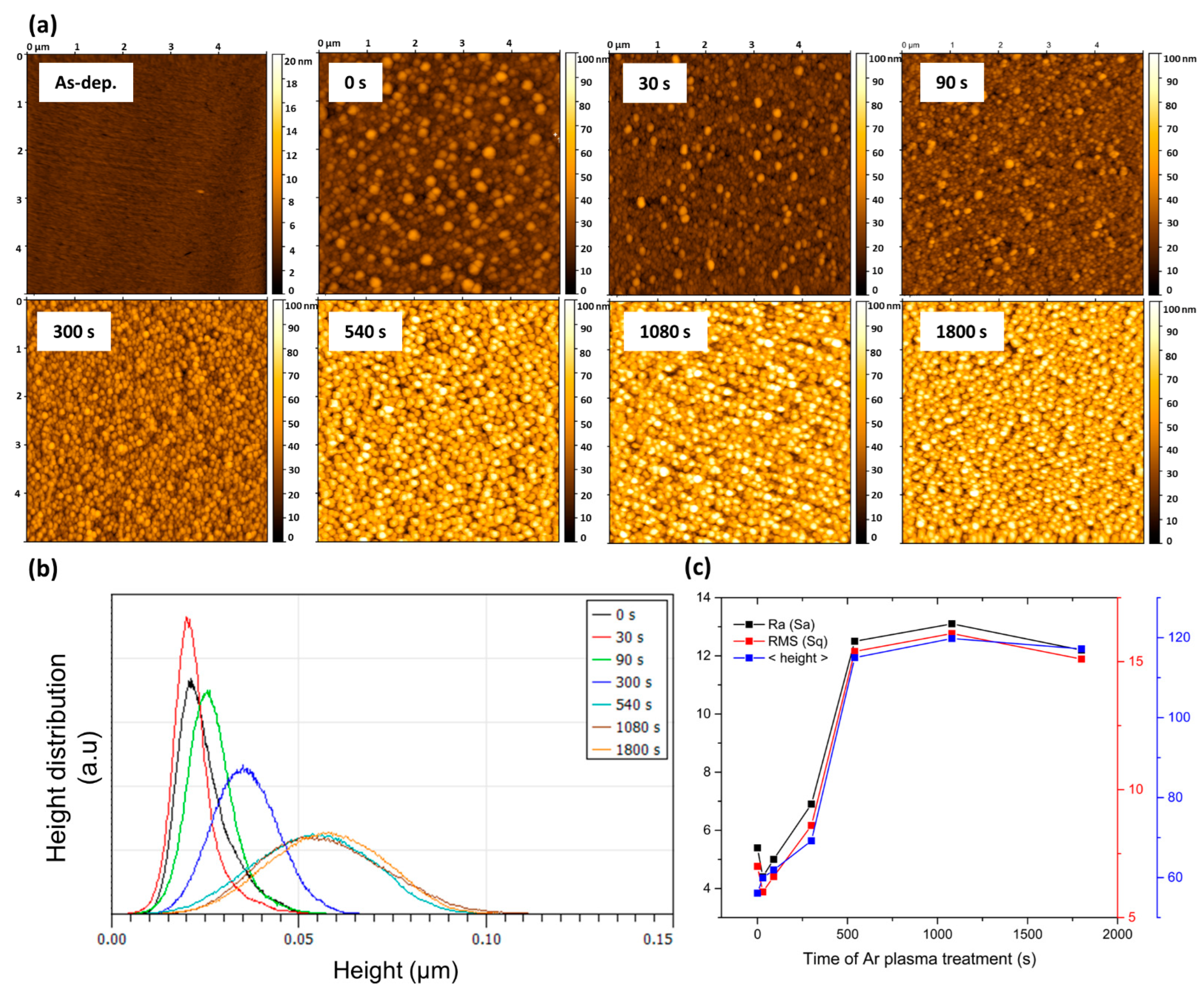
3.1. The Effect of Ar Plasma Etching on the Surface Properties of Au:CuO thin Films-Characterization of the Thin Films
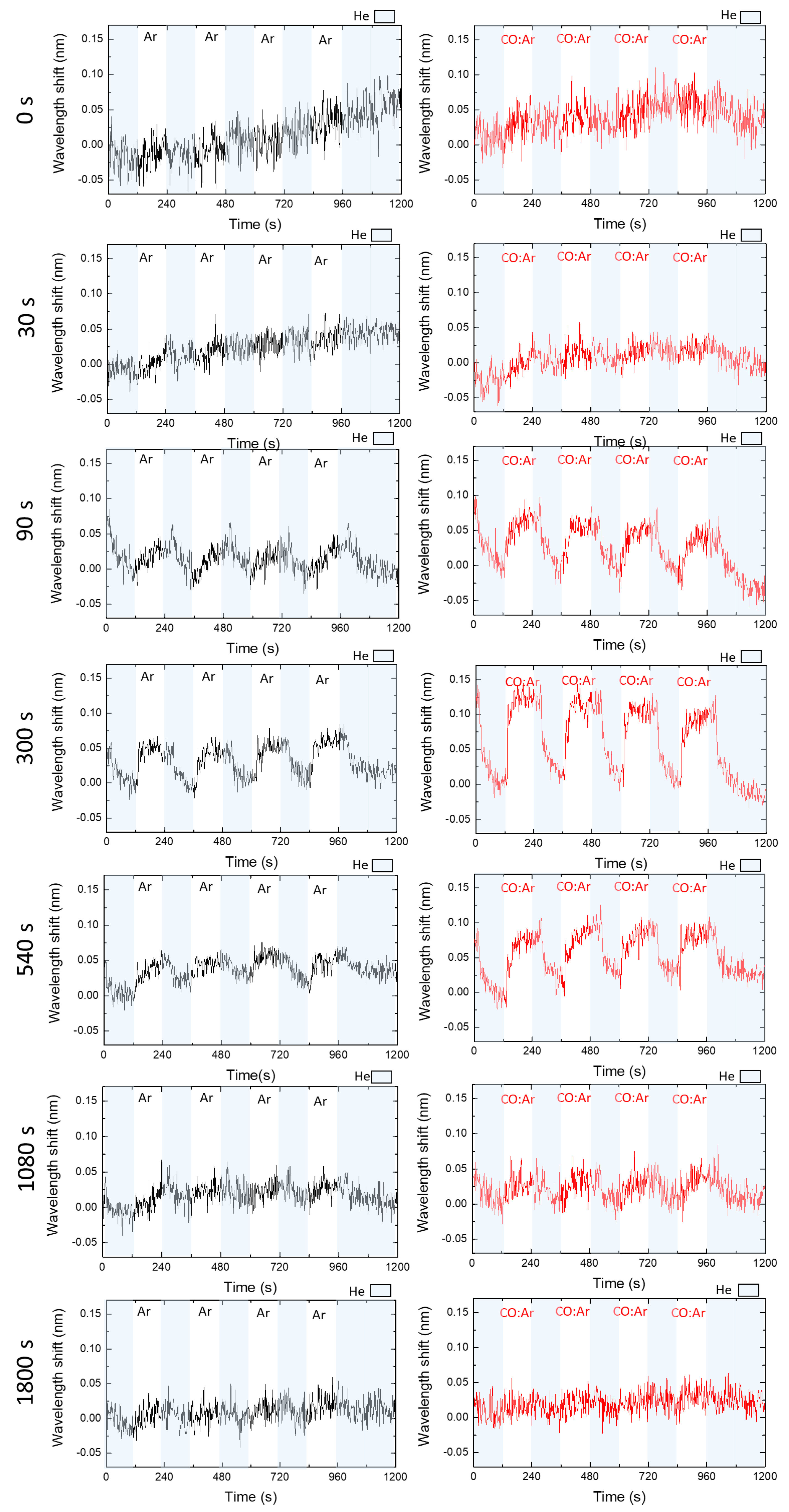
3.2. Gas Sensors Optimization—Gas Sensing Tests
4. Conclusions
Supplementary Materials
Author Contributions
Funding
Institutional Review Board Statement
Informed Consent Statement
Data Availability Statement
Conflicts of Interest
References
- Song, M.; Wang, D.; Peana, S.; Choudhury, S.; Nyga, P.; Kudyshev, Z.A.; Yu, H.; Boltasseva, A.; Shalaev, V.M.; Kildishev, A.V. Colors with Plasmonic Nanostructures: A Full-Spectrum Review. Appl. Phys. Rev. 2019, 6, 041308. [Google Scholar] [CrossRef]
- Mohan Bhagyaraj, S.; Oluwafemi, O.S. Nanotechnology: The Science of the Invisible. In Synthesis of Inorganic Nanomaterials; Woodhead Publishing: Sawston, UK, 2018; pp. 1–18. [Google Scholar] [CrossRef]
- Liu, M.; Kang, Q.; Xie, Z.; Lu, L.; Dai, K.; Dawson, G. Heterostructure Nanocomposite with Local Surface Plasmon Resonance Effect Enhanced Photocatalytic Activity—A Critical Review. J. Phys. D. Appl. Phys. 2022, 55, 043002. [Google Scholar] [CrossRef]
- Yang, Z.; Sassa, F.; Hayashi, K. A Robot Equipped with a High-Speed LSPR Gas Sensor Module for Collecting Spatial Odor Information from on-Ground Invisible Odor Sources. ACS Sens. 2018, 3, 1174–1181. [Google Scholar] [CrossRef] [PubMed]
- Oh, S.Y.; Heo, N.S.; Shukla, S.; Cho, H.J.; Vilian, A.T.E.; Kim, J.; Lee, S.Y.; Han, Y.K.; Yoo, S.M.; Huh, Y.S. Development of Gold Nanoparticle-Aptamer-Based LSPR Sensing Chips for the Rapid Detection of Salmonella Typhimurium in Pork Meat. Sci. Rep. 2017, 7, 10130. [Google Scholar] [CrossRef]
- Chen, B.; Liu, C.; Shang, L.; Guo, H.; Qin, J.; Ge, L.; Jing, C.J.; Feng, C.; Hayashi, K. Electric-Field Enhancement of Molecularly Imprinted Sol-Gel-Coated Au Nano-Urchin Sensors for Vapor Detection of Plant Biomarkers. J. Mater. Chem. C 2019, 8, 262–269. [Google Scholar] [CrossRef]
- Huang, Z.; Meng, G.; Hu, X.; Pan, Q.; Huo, D.; Zhou, H.; Ke, Y.; Wu, N. Plasmon-Tunable Au@Ag Core-Shell Spiky Nanoparticles for Surface-Enhanced Raman Scattering. Nano Res. 2019, 12, 449–455. [Google Scholar] [CrossRef]
- Do, P.Q.T.; Huong, V.T.; Phuong, N.T.T.; Nguyen, T.H.; Ta, H.K.T.; Ju, H.; Phan, T.B.; Phung, V.D.; Trinh, K.T.L.; Tran, N.H.T. The Highly Sensitive Determination of Serotonin by Using Gold Nanoparticles (Au NPs) with a Localized Surface Plasmon Resonance (LSPR) Absorption Wavelength in the Visible Region. RSC Adv. 2020, 10, 30858–30869. [Google Scholar] [CrossRef]
- Amendola, V.; Pilot, R.; Frasconi, M.; Maragò, O.M.; Iatì, M.A. Surface Plasmon Resonance in Gold Nanoparticles: A Review. J. Phys. Condens. Matter 2017, 29, 203002. [Google Scholar] [CrossRef]
- Jeong, H.H.; Choi, E.; Ellis, E.; Lee, T.C. Recent Advances in Gold Nanoparticles for Biomedical Applications: From Hybrid Structures to Multi-Functionality. J. Mater. Chem. B 2019, 7, 3480–3496. [Google Scholar] [CrossRef] [Green Version]
- Almawgani, A.H.M.; Daher, M.G.; Taya, S.A.; Olaimat, M.M.; Alhawari, A.R.H.; Colak, I. Detection of Blood Plasma Concentration Theoretically Using SPR-Based Biosensor Employing Black Phosphor Layers and Different Metals. Plasmonics 2022, 17, 1751–1764. [Google Scholar] [CrossRef]
- Wang, L.; Hasanzadeh Kafshgari, M.; Meunier, M. Optical Properties and Applications of Plasmonic-Metal Nanoparticles. Adv. Funct. Mater. 2020, 30, 2005400. [Google Scholar] [CrossRef]
- Rodrigues, M.S.; Costa, D.; Domingues, R.P.; Apreutesei, M.; Pedrosa, P.; Martin, N.; Correlo, V.M.; Reis, R.L.; Alves, E.; Barradas, N.P.; et al. Optimization of Nanocomposite Au/TiO2 Thin Films towards LSPR Optical-Sensing. Appl. Surf. Sci. 2018, 438, 74–83. [Google Scholar] [CrossRef]
- Bhalla, N.; Jain, A.; Lee, Y.; Shen, A.Q.; Lee, D. Dewetting Metal Nanofilms—Effect of Substrate on Refractive Index Sensitivity of Nanoplasmonic Gold. Nanomaterials 2019, 9, 1530. [Google Scholar] [CrossRef] [PubMed]
- Proença, M.; Borges, J.; Rodrigues, M.S.; Meira, D.I.; Sampaio, P.; Dias, J.P.; Pedrosa, P.; Martin, N.; Bundaleski, N.; Teodoro, O.M.N.D.; et al. Nanocomposite Thin Films Based on Au-Ag Nanoparticles Embedded in a CuO Matrix for Localized Surface Plasmon Resonance Sensing. Appl. Surf. Sci. 2019, 484, 152–168. [Google Scholar] [CrossRef]
- Montaño-Priede, J.L.; Peña-Rodríguez, O.; Pal, U. Near-Electric-Field Tuned Plasmonic Au@SiO2 and Ag@SiO2 Nanoparticles for Efficient Utilization in Luminescence Enhancement and Surface-Enhanced Spectroscopy. J. Phys. Chem. C 2017, 121, 23062–23071. [Google Scholar] [CrossRef]
- Song, Y.; Tran, V.T.; Lee, J. Tuning Plasmon Resonance in Magnetoplasmonic Nanochains by Controlling Polarization and Interparticle Distance for Simple Preparation of Optical Filters. ACS Appl. Mater. Interfaces 2017, 9, 24433–24439. [Google Scholar] [CrossRef] [PubMed]
- Ginsburg, A.; Priel, M.; Barad, H.N.; Keller, D.A.; Borvick, E.; Rietwyk, K.; Kama, A.; Meir, S.; Anderson, A.Y.; Zaban, A. Solid State ITO|Au-NPs|TiO2 Plasmonic Based Solar Cells. Sol. Energy Mater. Sol. Cells 2018, 179, 254–259. [Google Scholar] [CrossRef]
- Ghodselahi, T.; Neishaboorynejad, T.; Arsalani, S. Fabrication LSPR Sensor Chip of Ag NPs and Their Biosensor Application Based on Interparticle Coupling. Appl. Surf. Sci. 2015, 343, 194–201. [Google Scholar] [CrossRef]
- Duan, Q.; Liu, Y.; Chang, S.; Chen, H.; Chen, J.H. Surface Plasmonic Sensors: Sensing Mechanism and Recent Applications. Sensors 2021, 21, 5262. [Google Scholar] [CrossRef]
- Kim, D.M.; Park, J.S.; Jung, S.W.; Yeom, J.; Yoo, S.M. Biosensing Applications Using Nanostructure-Based Localized Surface Plasmon Resonance Sensors. Sensors 2021, 21, 3191. [Google Scholar] [CrossRef]
- Shang, L.; Liu, C.; Watanabe, M.; Chen, B.; Hayashi, K. LSPR Sensor Array Based on Molecularly Imprinted Sol-Gels for Pattern Recognition of Volatile Organic Acids. Sens. Actuators B Chem. 2017, 249, 14–21. [Google Scholar] [CrossRef]
- Chen, L.; Wu, B.; Guo, L.; Tey, R.; Huang, Y.; Kim, D.-H. A Single-Nanoparticle NO2 Gas Sensor Constructed Using Active Molecular Plasmonics. Chem. Commun. 2015, 51, 1326–1329. [Google Scholar] [CrossRef] [PubMed]
- Takimoto, Y.; Monkawa, A.; Nagata, K.; Kobayashi, M.; Kinoshita, M.; Gessei, T.; Mori, T.; Kagi, H. Detection of SO2 at the Ppm Level with Localized Surface Plasmon Resonance (LSPR) Sensing. Plasmonics 2020, 15, 805–811. [Google Scholar] [CrossRef]
- Shang, L.; Liu, C.; Chen, B.; Hayashi, K. Development of Molecular Imprinted Sol-Gel Based LSPR Sensor for Detection of Volatile Cis-Jasmone in Plant. Sens. Actuators B Chem. 2018, 260, 617–626. [Google Scholar] [CrossRef]
- Proença, M.; Rodrigues, M.S.; Borges, J.; Vaz, F. Optimization of Au:CuO Nanocomposite Thin Films for Gas Sensing with High-Resolution Localized Surface Plasmon Resonance Spectroscopy. Anal. Chem. 2020, 92, 4349–4356. [Google Scholar] [CrossRef]
- Chen, P.; Liedberg, B. Curvature of the Localized Surface Plasmon Resonance Peak. Anal. Chem. 2014, 86, 7399–7405. [Google Scholar] [CrossRef]
- Rodrigues, M.S.; Borges, J.; Lopes, C.; Pereira, R.M.S.; Vasilevskiy, M.I.; Vaz, F. Gas Sensors Based on Localized Surface Plasmon Resonances: Synthesis of Oxide Films with Embedded Metal Nanoparticles, Theory and Simulation, and Sensitivity Enhancement Strategies. Appl. Sci. 2021, 11, 5388. [Google Scholar] [CrossRef]
- Guo, L.; Jackman, J.A.; Yang, H.H.; Chen, P.; Cho, N.J.; Kim, D.H. Strategies for Enhancing the Sensitivity of Plasmonic Nanosensors. Nano Today 2015, 10, 213–239. [Google Scholar] [CrossRef]
- Xu, T.; Geng, Z. Strategies to Improve Performances of LSPR Biosensing: Structure, Materials, and Interface Modification. Biosens. Bioelectron. 2021, 174, 112850. [Google Scholar] [CrossRef]
- Qi, X.; Bi, J. Plasmonic Sensors Relying on Nanoparticle Arrays Created by a Template-Directed Dewetting Process. Opt. Commun. 2019, 453, 124328. [Google Scholar] [CrossRef]
- Chung, T.; Lee, S.Y.; Song, E.Y.; Chun, H.; Lee, B. Plasmonic Nanostructures for Nano-Scale Bio-Sensing. Sensors 2011, 11, 10907–10929. [Google Scholar] [CrossRef] [PubMed]
- Yang, W.C.; Chen, Y.X.; Fu, T.Y.; Peng, S.; Du, C.L.; Lu, Y.G.; Shi, D.N. The Cross-Section Shape-Dependent Responses of S and FOM of Individual Au Nanorod Sensors. Appl. Phys. A Mater. Sci. Process. 2019, 125, 345. [Google Scholar] [CrossRef]
- Galopin, E.; Niedziółka-Jönsson, J.; Akjouj, A.; Pennec, Y.; Djafari-Rouhani, B.; Noual, A.; Boukherroub, R.; Szunerits, S. Sensitivity of Plasmonic Nanostructures Coated with Thin Oxide Films for Refractive Index Sensing: Experimental and Theoretical Investigations. J. Phys. Chem. C 2010, 114, 11769–11775. [Google Scholar] [CrossRef]
- Rodrigues, M.S.; Borges, J.; Vaz, F. Enhancing the Sensitivity of Nanoplasmonic Thin Films for Ethanol Vapor Detection. Materials 2020, 13, 870. [Google Scholar] [CrossRef]
- Rodrigues, M.S.; Borges, J.; Proença, M.; Pedrosa, P.; Martin, N.; Romanyuk, K.; Kholkin, A.L.; Vaz, F. Nanoplasmonic Response of Porous Au-TiO 2 Thin Films Prepared by Oblique Angle Deposition. Nanotechnology 2019, 30, 225701. [Google Scholar] [CrossRef]
- Zhou, Y.; Zou, C.; Lin, X.; Guo, Y. UV Light Activated NO2 Gas Sensing Based on Au Nanoparticles Decorated Few-Layer MoS2 Thin Film at Room Temperature. Appl. Phys. Lett. 2018, 113, 082103. [Google Scholar] [CrossRef]
- Wuenschell, J.K.; Jee, Y.; Lau, D.K.; Yu, Y.; Ohodnicki, P.R. Combined Plasmonic Au-Nanoparticle and Conducting Metal Oxide High-Temperature Optical Sensing with LSTO. Nanoscale 2020, 12, 14524–14537. [Google Scholar] [CrossRef]
- Sowmya, B.; John, A.; Panda, P.K. A Review on Metal-Oxide Based p-n and n-n Heterostructured Nano-Materials for Gas Sensing Applications. Sens. Int. 2021, 2, 100085. [Google Scholar] [CrossRef]
- Samransuksamer, B.; Horprathum, M.; Eiamchai, P.; Patthanasettakul, V.; Wisitsoraat, A.; Chananonnawathorn, C.; Phokharatkul, D.; Chindaudom, P.; Jutarosaga, T.; Rakreungdet, W.; et al. Decoration of Gold Nanoparticles on TiO2 Thin Films for Enhanced Response of Ethanol Gas Sensors. In Advanced Materials Research; Trans Tech Publications Ltd.: Wollerau, Switzerland, 2014; Volume 979, pp. 251–254. [Google Scholar]
- Lopez, G.A.; Estevez, M.C.; Soler, M.; Lechuga, L.M. Recent Advances in Nanoplasmonic Biosensors: Applications and Lab-on-a-Chip Integration. Nanophotonics 2017, 6, 123–136. [Google Scholar] [CrossRef]
- Kedem, O.; Vaskevich, A.; Rubinstein, I. Critical Issues in Localized Plasmon Sensing. J. Phys. Chem. C 2014, 118, 8227–8244. [Google Scholar] [CrossRef]
- Zalyubovskiy, S.J.; Bogdanova, M.; Deinega, A.; Lozovik, Y.; Pris, A.D.; An, K.H.; Hall, W.P.; Potyrailo, R.A. Theoretical Limit of Localized Surface Plasmon Resonance Sensitivity to Local Refractive Index Change and Its Comparison to Conventional Surface Plasmon Resonance Sensor. J. Opt. Soc. Am. A 2012, 29, 994–1002. [Google Scholar] [CrossRef] [PubMed]
- Ozhikandathil, J.; Packirisamy, M. Simulation and Implementation of a Morphology-Tuned Gold Nano-Islands Integrated Plasmonic Sensor. Sensors 2014, 14, 10497–10513. [Google Scholar] [CrossRef] [PubMed]
- Meira, D.I.; Domingues, R.P.; Rodrigues, M.S.; Alves, E.; Barradas, N.P.; Borges, J.; Vaz, F. Thin Films of Au-Al2O3 for Plasmonic Sensing. Appl. Surf. Sci. 2020, 500, 144035. [Google Scholar] [CrossRef]
- Pedrueza, E.; Sancho-Parramon, J.; Bosch, S.; Valdés, J.L.; Martinez-Pastor, J.P. Plasmonic Layers Based on Au-Nanoparticle-Doped TiO2 for Optoelectronics: Structural and Optical Properties. Nanotechnology 2013, 24, 065202. [Google Scholar] [CrossRef]
- Proenca, M.; Rodrigues, M.; Vaz, F.; Borges, J. Carbon Monoxide (CO) Sensor Based on Au Nanoparticles Embedded in a CuO Matrix by HR-LSPR Spectroscopy at Room Temperature. IEEE Sens. Lett. 2021, 5, 1–3. [Google Scholar] [CrossRef]
- Proença, M.; Rodrigues, M.S.; Borges, J.; Vaz, F. Gas Sensing with Nanoplasmonic Thin Films Composed of Nanoparticles (Au, Ag) Dispersed in a CuO Matrix. Coatings 2019, 9, 337. [Google Scholar] [CrossRef]
- Molodtsov, S.L.; Gurbich, A.F.; Jeynes, C. Accurate Ion Beam Analysis in the Presence of Surface Roughness. J. Phys. D. Appl. Phys. 2008, 41, 205303. [Google Scholar] [CrossRef]
- Barradas, N.P.; Jeynes, C.; Webb, R.P.; Kreissig, U.; Grötzschel, R. Unambiguous Automatic Evaluation of Multiple Ion Beam Analysis Data with Simulated Annealing. In Nuclear Instruments and Methods in Physics Research Section B: Beam Interactions with Materials and Atoms; Elsevier: Amsterdam, The Netherlands, 1999; Volume 149, pp. 233–237. [Google Scholar] [CrossRef]
- Rodrigues, M.S.; Pereira, R.M.S.; Vasilevskiy, M.I.; Borges, J.; Vaz, F. NANOPTICS: In-Depth Analysis of NANomaterials for OPTICal Localized Surface Plasmon Resonance Sensing. SoftwareX 2020, 12, 100522. [Google Scholar] [CrossRef]
- Joo, Y.H.; Um, D.S.; Kim, C.I. Tunable Physical Properties of Al-Doped ZnO Thin Films by O2 and Ar Plasma Treatments. Mater. Res. Express 2021, 8, 126402. [Google Scholar] [CrossRef]
- Hammad, T.M.; Tamous, H.M.; Hejazy, N.K. Effect of Argon–Plasma Treatment on the Electrical and Optical Properties of Sol–Gel Antimony-Doped Tin Dioxide Thin Films Fabricated By Dip Coating. Int. J. Mod. Phys. B 2012, 21, 4399–4406. [Google Scholar] [CrossRef]
- Hwang, D.K.; Misra, M.; Lee, Y.E.; Baek, S.D.; Myoung, J.M.; Lee, T.I. The Role of Ar Plasma Treatment in Generating Oxygen Vacancies in Indium Tin Oxide Thin Films Prepared by the Sol-Gel Process. Appl. Surf. Sci. 2017, 405, 344–349. [Google Scholar] [CrossRef]
- Mahmoud, M.A.; Chamanzar, M.; Adibi, A.; El-Sayed, M.A. Effect of the Dielectric Constant of the Surrounding Medium and the Substrate on the Surface Plasmon Resonance Spectrum and Sensitivity Factors of Highly Symmetric Systems: Silver Nanocubes. J. Am. Chem. Soc. 2012, 134, 6434–6442. [Google Scholar] [CrossRef] [PubMed]
- Borges, J.; Ferreira, C.G.; Fernandes, J.P.C.; Rodrigues, M.S.; Proença, M.; Apreutesei, M.; Alves, E.; Barradas, N.P.; Moura, C.; Vaz, F. Thin Films of Ag-Au Nanoparticles Dispersed in TiO2: Influence of Composition and Microstructure on the LSPR and SERS Responses. J. Phys. D. Appl. Phys. 2018, 51, 205102. [Google Scholar] [CrossRef]
- Mardiansyah, D.; Badloe, T.; Triyana, K.; Mehmood, M.Q.; Raeis-Hosseini, N.; Lee, Y.; Sabarman, H.; Kim, K.; Rho, J. Effect of Temperature on the Oxidation of Cu Nanowires and Development of an Easy to Produce, Oxidation-Resistant Transparent Conducting Electrode Using a PEDOT:PSS Coating. Sci. Rep. 2018, 8, 10639. [Google Scholar] [CrossRef] [PubMed]
- Akgul, F.A.; Akgul, G.; Yildirim, N.; Unalan, H.E.; Turan, R. Influence of Thermal Annealing on Microstructural, Morphological, Optical Properties and Surface Electronic Structure of Copper Oxide Thin Films. Mater. Chem. Phys. 2014, 147, 987–995. [Google Scholar] [CrossRef]
- Purusottam-Reddy, B.; Sivajee-Ganesh, K.; Jayanth-Babu, K.; Hussain, O.M.; Julien, C.M. Microstructure and Supercapacitive Properties of Rf-Sputtered Copper Oxide Thin Films: Influence of O2/Ar Ratio. Ionics 2015, 21, 2319–2328. [Google Scholar] [CrossRef]
- Choudhary, S.; Sarma, J.V.N.; Pande, S.; Ababou-Girard, S.; Turban, P.; Lepine, B.; Gangopadhyay, S. Oxidation Mechanism of Thin Cu Films: A Gateway towards the Formation of Single Oxide Phase. AIP Adv. 2018, 8, 055114. [Google Scholar] [CrossRef]
- Kumar, B.R.; Rao, T.S. AFM Studies on Surface Morphology, Topography and Texture of Nanostructured Zinc Aluminum Oxide Thin Films. Dig. J. Nanomater. Biostructures 2012, 7, 1881–1889. [Google Scholar]
- Proença, M.; Borges, J.; Rodrigues, M.S.; Domingues, R.P.; Dias, J.P.; Trigueiro, J.; Bundaleski, N.; Teodoro, O.M.N.D.; Vaz, F. Development of Au/CuO Nanoplasmonic Thin Films for Sensing Applications. Surf. Coat. Technol. 2018, 343, 178–185. [Google Scholar] [CrossRef]
- Gowthaman, N.S.K.; Shankar, S.; Abraham John, S. Substrate Catalyzed Formation of Au-Cu Bimetallic Nanoparticles as Electrocatalyst for the Reduction of Dioxygen and Hydrogen Peroxide. J. Electroanal. Chem. 2018, 812, 37–44. [Google Scholar] [CrossRef]
- Mayer, K.M.; Hafner, J.H. Localized Surface Plasmon Resonance Sensors. Chem. Rev. 2011, 111, 3828–3857. [Google Scholar] [CrossRef] [PubMed]
- Ghodselahi, T.; Zahrabi, H.; Saani, M.H.; Vesaghi, M.A. CO Gas Sensor Properties of Cu@CuO Core-Shell Nanoparticles Based on Localized Surface Plasmon Resonance. J. Phys. Chem. C 2011, 115, 22126–22130. [Google Scholar] [CrossRef]
- Wei, C.; Liu, Q. Shape-, Size-, and Density-Tunable Synthesis and Optical Properties of Copper Nanoparticles. CrystEngComm 2017, 19, 3254–3262. [Google Scholar] [CrossRef]
- El Barghouti, M.; Akjouj, A.; Mir, A. Effect of MoS2 Layer on the LSPR in Periodic Nanostructures. Optik 2018, 171, 237–246. [Google Scholar] [CrossRef]
- Djurić, Z.; Jokić, I.; Milovanović, G. Signal-to-Noise Ratio in Adsorption-Based Microfluidic Bio/Chemical Sensors. Procedia Eng. 2016, 168, 642–645. [Google Scholar] [CrossRef]


| Time of Ar Plasma Treatment (s) | AFM 5 × 5 µm | SEM | |||||
|---|---|---|---|---|---|---|---|
| Ra (Sa) (nm) | RMS (Sq) (nm) | <Height> (nm) | NPs Count | <Feret Diameter> (nm) | <Nearest Neighbor> (nm) | Av. Aspect Ratio | |
| 0 | 5.4 | 7.0 | 56.1 | 120 | 51 (σ = 29) | 47 (σ = 19) | 1.35 (σ = 0.5) |
| 30 | 4.4 | 6.0 | 59.9 | 128 | 48 (σ = 28) | 46 (σ = 19) | 1.43 (σ = 0.6) |
| 90 | 5.0 | 6.6 | 61.9 | 179 | 41 (σ = 26) | 38 (σ = 14) | 1.46 (σ = 0.9) |
| 300 | 6.9 | 8.6 | 69.2 | 145 | 48 (σ = 25) | 43 (σ = 15) | 1.36 (σ = 0.6) |
| 540 | 12.5 | 15.4 | 115.0 | 133 | 50 (σ = 30) | 40 (σ = 19) | 1.46 (σ = 0.5) |
| 1080 | 13.1 | 16.1 | 119.8 | 142 | 46 (σ = 27) | 44 (σ = 15) | 1.58 (σ = 1) |
| 1800 | 12.2 | 15.1 | 117.2 | 143 | 45 (σ = 27) | 42 (σ = 18) | 1.46 (σ = 0.6) |
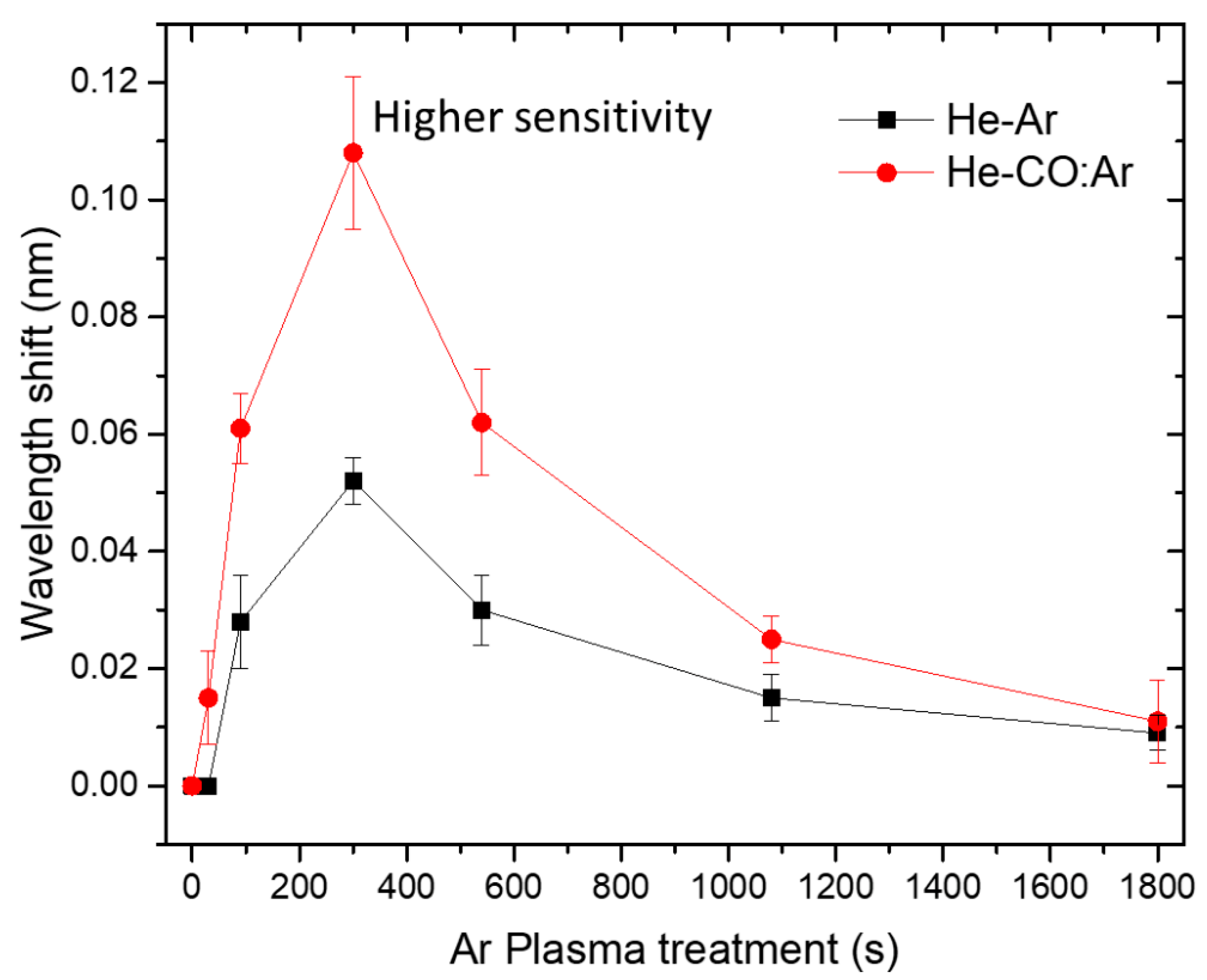
| Time of Ar Plasma Treatment (s) | Average Wavelength Band Shift (nm) He-Ar | SNR He-Ar | Average Wavelength Band Shift (nm) He-CO:Ar | SNR He-CO:Ar | RIS (He-Ar) |
|---|---|---|---|---|---|
| 0 | 0 | 0 | 0 | 0 | 0 |
| 30 | 0 | 0 | 0.015 ± 0.008 | 1.4 | 0 |
| 90 | 0.028 ± 0.008 | 1.8 | 0.061 ± 0.006 | 3.9 | 457 ± 130 |
| 300 | 0.052 ± 0.004 | 3.2 | 0.108 ± 0.013 | 6.7 | 849 ± 65 |
| 540 | 0.03 ± 0.006 | 2.3 | 0.062 ± 0.009 | 3.6 | 490 ± 98 |
| 1080 | 0.015 ± 0.004 | 1.3 | 0.025 ± 0.004 | 1.6 | 245 ± 65 |
| 1800 | 0.009 ± 0.003 | 1.1 | 0.011 ± 0.007 | 1.1 | 147 ± 49 |
Publisher’s Note: MDPI stays neutral with regard to jurisdictional claims in published maps and institutional affiliations. |
© 2022 by the authors. Licensee MDPI, Basel, Switzerland. This article is an open access article distributed under the terms and conditions of the Creative Commons Attribution (CC BY) license (https://creativecommons.org/licenses/by/4.0/).
Share and Cite
Proença, M.; Rodrigues, M.S.; Meira, D.I.; Castro, M.C.R.; Rodrigues, P.V.; Machado, A.V.; Alves, E.; Barradas, N.P.; Borges, J.; Vaz, F. Optimization of Au:CuO Thin Films by Plasma Surface Modification for High-Resolution LSPR Gas Sensing at Room Temperature. Sensors 2022, 22, 7043. https://doi.org/10.3390/s22187043
Proença M, Rodrigues MS, Meira DI, Castro MCR, Rodrigues PV, Machado AV, Alves E, Barradas NP, Borges J, Vaz F. Optimization of Au:CuO Thin Films by Plasma Surface Modification for High-Resolution LSPR Gas Sensing at Room Temperature. Sensors. 2022; 22(18):7043. https://doi.org/10.3390/s22187043
Chicago/Turabian StyleProença, Manuela, Marco S. Rodrigues, Diana I. Meira, M. Cidalia R. Castro, Pedro V. Rodrigues, Ana V. Machado, Eduardo Alves, Nuno P. Barradas, Joel Borges, and Filipe Vaz. 2022. "Optimization of Au:CuO Thin Films by Plasma Surface Modification for High-Resolution LSPR Gas Sensing at Room Temperature" Sensors 22, no. 18: 7043. https://doi.org/10.3390/s22187043