Abstract
In this paper, an optimal design of a high-efficiency DC-DC boost converter is proposed for RF energy harvesting Internet of Things (IoT) sensors. Since the output DC voltage of the RF-DC rectifier for RF energy harvesting varies considerably depending on the RF input power, the DC-DC boost converter following the RF-DC rectifier is required to achieve high power conversion efficiency (PCE) in a wide input voltage range. Therefore, based on the loss analysis and modeling of an inductor-based DC-DC boost converter, an optimal design method of design parameters, including inductance and peak inductor current, is proposed to obtain the maximum PCE by minimizing the total loss according to different input voltages in a wide input voltage range. A high-efficiency DC-DC boost converter for RF energy harvesting applications is designed using a 65 nm CMOS process. The modeled total losses agree well with the circuit simulation results and the proposed loss modeling results accurately predict the optimal design parameters to obtain the maximum PCE. Based on the proposed loss modeling, the optimally designed DC-DC boost converter achieves a power conversion efficiency of 96.5% at a low input voltage of 0.1 V and a peak efficiency of 98.4% at an input voltage of 0.4 V.
1. Introduction
Energy harvesting technology is considered a key technology for battery-free Internet of Things (IoT) devices [,,]. Since RF signals of various frequency bands such as 5G, Wi-Fi, and TV exist around us, RF energy harvesting can be a very useful energy source [,,,,]. However, when the available power of the surrounding RF signal is low, the output DC voltage of the RF rectifier is lower than the voltage required by the system, making it difficult to use as a power source. To increase the DC output voltage, a multi-stage rectifier is required, which significantly reduces the efficiency of energy harvesting [].
Therefore, the proposed RF energy harvesting system adopts a DC-DC boost converter to convert the low output voltage of the RF-DC rectifier into a high voltage of 1 V or more. Figure 1 shows a block diagram of an RF energy harvesting system consisting of an RF energy harvesting RF-DC rectifier and a DC-DC boost converter. The power management circuit for RF energy harvesting system consists of an RF-DC rectifier that harvests ambient RF energy and converts it to DC voltage, and a DC-DC boost converter that boosts the voltage to a higher DC voltage and supplies it to the load.
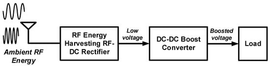
Figure 1.
Block diagram of RF energy harvesting system consisting of RF energy harvesting RF-DC rectifier and DC-DC boost converter.
1.1. Main Contribution
Since the output DC voltage of the RF-DC rectifier for RF energy harvesting varies greatly depending on the RF input power, the DC-DC boost converter is required to achieve high power conversion efficiency (PCE) in a wide input voltage range [,,,,,]. Therefore, to obtain high PCE for different input voltages in a wide input voltage range, an optimal design method of design parameters including an optimal peak inductor current design according to the input voltage is required.
In this paper, we propose an optimal design methodology to achieve high efficiency in a wide input voltage range based on loss analysis and modeling of an inductor-based DC-DC boost converter. In the proposed efficiency optimization design methodology of the DC-DC boost converter, each loss component of the inductor-based DC-DC boost converter is analyzed and the loss modeling result according to the design parameters is presented. Based on the loss analysis and modeling, optimum design parameters including inductance and peak inductor current are obtained to achieve the maximum PCE by minimizing the total loss according to different input voltages in a wide input voltage range.
1.2. Organization
This paper is organized as follows. Section 2 introduces the previous DC-DC boost converters for energy harvesting. Section 3 introduces the efficiency problem and the system model of an inductor-based DC-DC boost converter. Section 4 presents loss analysis and modeling of the boost converter. Section 5 focuses on the design methodology for optimizing power conversion efficiency. Section 6 highlights the circuit simulation results. Finally, concluding remarks are given in Section 7.
2. Previous DC-DC Boost Converters for Energy Harvesting
DC-DC boost converters based on transformers, switched capacitors, and inductors are used to convert a low input voltage to a high voltage for energy harvesting applications. The transformer-based boost converter operates at a low input voltage of 21 mV without a separate start-up circuit [], but the transformer increases the area and reduces efficiency at low input voltages. Capacitive-based boost converters are advantageous for on-chip integration because they do not require an inductor and have a relatively small physical form factor [,,,]. A capacitive-based boost converter with a dynamic body biasing technique that operates at a low input voltage of 0.15 V without a start-up circuit has been demonstrated in []. However, it has a limited voltage conversion ratio and relatively low power conversion efficiency at low input voltage. Inductor-based converters are difficult to integrate on-chip due to off-chip inductors but operate at a relatively low input voltage and achieve high power conversion efficiency in a low input voltage range compared with capacitive-based boost converters [].
In recent works, several approaches have been proposed to improve the power conversion efficiency of low input voltage boost converters for thermoelectric energy harvesting [,,,,,,,]. In [,], high conversion efficiency is achieved by applying an adaptive gate biasing technique and a peak inductor current control scheme, respectively. However, these designs achieve high efficiency at relatively high input power levels of hundreds of μW or more. In [], a loss optimization design for MOS switch width and switching frequency has been reported to minimize the total loss to achieve high efficiency in a DC-DC boost converter. In [], an optimization method for finding the optimum switching frequency, inductance value, and switch size of the converter has been reported. However, these methods obtain high efficiency in a specific input voltage range for thermoelectric energy harvesting, and the efficiency is significantly reduced in a wide input voltage range outside this range.
3. Efficiency Problem and System Model of DC-DC Boost Converter
3.1. Efficiency Problem in Boost Converter for RF Energy Harvesting
Ambient RF energy harvesting is one of the very useful energy sources for IoT devices, but, when the power of available ambient RF signals is low, the output DC voltage of the RF rectifier is lower than the voltage required by the system, making it difficult to use it as a power source [,,]. Therefore, the proposed RF energy harvesting system adopts a DC-DC boost converter to increase the low output voltage of the RF-DC rectifier to a voltage higher than 1 V. Since the output DC voltage of the RF-DC rectifier for harvesting ambient RF energy varies greatly depending on the RF input power, the voltage applied to the following DC-DC boost converter has a wide input voltage range depending on the ambient RF input power. However, conventional DC-DC boost converters that achieve peak power conversion efficiency (PCE) at a specific input voltage have a problem in that PCE significantly degrades over a wide input voltage range. Therefore, to obtain a high PCE for different input voltages in a wide input voltage range, a design method for optimizing design parameters, including optimal peak inductor current and inductance design according to the input voltage, is required.
3.2. System Model of DC-DC Boost Converter
Figure 2 shows an inductor-based DC-DC boost converter circuit employed to boost the low output DC voltage of the RF rectifier to the high DC voltage required by the circuit in a low power ambient RF energy harvesting operation. The DC-DC boost converter consists of input inductor L, NMOS switch M1, PMOS switch M2, and a control circuit that drives the switches.
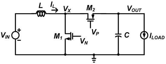
Figure 2.
Schematic of an inductor-based DC-DC boost converter.
For low input voltage operation, it is more efficient to operate in discontinuous conduction mode (DCM) []. Figure 3 shows the DCM operation and inductor current (IL) waveform of the DC-DC boost converter. The DCM operation of the DC-DC boost converter has three stages: on time (TON), off time (TOFF), and dead time (TDEAD). During the on-time phase, the NMOS switch M1 turns on and the PMOS switch M2 turns off. In this phase, the current through the inductor IL increases at a constant slope up to the peak inductor current (IP), so magnetic energy is stored in the inductor. As the output capacitor C is discharged by the constant load current source, the output voltage decreases with a constant slope. During the off-time phase, switch M1 turns off and switch M2 turns on. In this phase, the output capacitor is not only discharged by the constant load current but also charged by the current flowing through the inductor. Thus, the energy in the inductor is transferred to the output load current (ILOAD) and output capacitor, and the inductor current decreases with a constant slope from IP to zero. During the dead-time phase, the PMOS switch M2 opens and the NMOS switch M1 remains open. In this phase, both the voltage across the inductor and the inductor current flowing through it are zero because both switches are open. The output of the converter is in the same state as the on-time phase, and the output voltage decreases with a constant slope as the output capacitor is discharged by the constant load current source. In DCM operation, the switching frequency is expressed in terms of inductance L and peak inductor current IP for given VIN, VOUT, and ILOAD conditions as
where ILOAD is the load current.
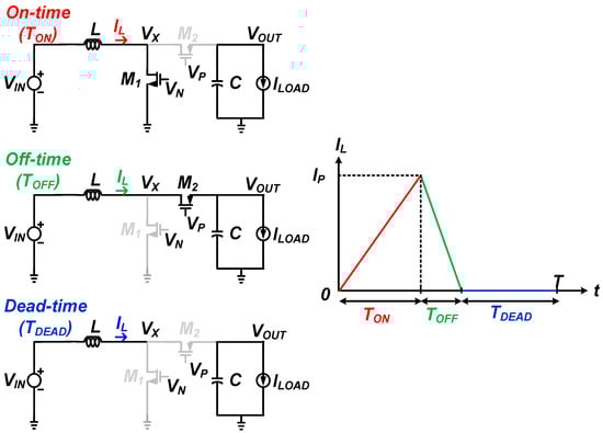
Figure 3.
DCM operation and inductor current (IL) waveform of DC-DC boost converter.
In the proposed efficiency optimization design methodology of the DC-DC boost converter, each loss component of the inductor-based DC-DC boost converter is analyzed and the loss modeling result according to the design parameters is presented. Based on the loss analysis and modeling, optimum design parameters that achieve maximum power conversion efficiency by minimizing the total loss according to different input voltages in a wide input voltage range are obtained. The power conversion efficiency (PCE) of the DC-DC boost converter is defined as:
where PIN and POUT are the input and output power of the converter, respectively, and PTOTAL represents the total losses of the converter including conduction loss due to equivalent series resistance (ESR) of the inductor, conduction loss due to switches, switching loss of NMOS and PMOS, and switching loss of buffer stages. The proposed design methodology to obtain the maximum PCE by minimizing the total loss according to different input voltages in a wide input voltage range is based on the loss analysis and modeling of an inductor-based DC-DC boost converter.
4. Loss Analysis and Modeling of DC-DC Boost Converter
The conduction loss due to the equivalent series resistance (ESR), RESR,L, of the inductor is expressed as:
The conduction loss of the switches is expressed as the sum of the losses due to the on resistance per unit width of the switches M1 and M2, RM1 and RM2, respectively, and the losses due to the leakage current per unit width of the switches M1 and M2, ILEAK,M1 and ILEAK,M2, respectively. The conduction loss due to the switches is expressed as:
where WM1 and WM2 are the widths of M1 and M2, respectively.
In the DC-DC boost converter, switching losses occur in the transition period by charging and discharging the NMOS and PMOS switch capacitances. The switching loss increases proportionally to the gate–drain capacitances per unit width of M1 and M2, CGD,M1 and CGD,M2, respectively, with the Miller effect, the drain–body capacitances per unit width of M1 and M2, CDB,M1 and CDB,M2, respectively, and the parasitic capacitance of the inductor, CL,PAR, expressed as:
Buffer stages are required as a driver circuit to drive NMOS and PMOS switches. Therefore, in addition to the power consumed to charge and discharge the gate capacitances of the NMOS and PMOS switches, CGS,M1 and CGS,M2, respectively, additional power is consumed by the buffer stages. The switching loss of the buffer stages is proportional to the gate equivalent capacitance of M1 and M2 with the Miller effect and is expressed as:
Therefore, the total loss of the DC-DC booster converter including conduction loss due to ESR of the inductor, conduction loss due to switches, switching loss of NMOS and PMOS, and switching loss of buffer stages, respectively, expressed in (3)–(6) is as follows.
Figure 4 shows the modeling results of each loss component of the boost converter according to the inductance L using (3)–(6) when VIN = 0.1 V, VOUT = 1 V, ILOAD = 1 mA, WM1 = WM2 = 20 mm, and IP = 30 mA. The inductor is designed as an off-chip component and the DCR of the inductor is modeled as a resistance value that increases with L. As shown in Figure 4, as the inductance increases, conduction loss of the inductor increases and switching loss and buffer loss decrease.
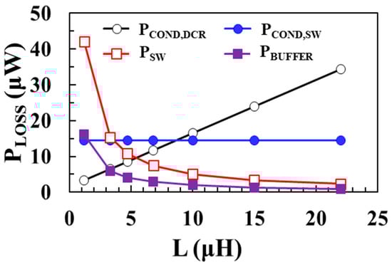
Figure 4.
Modeling results of each loss component according to inductance.
Figure 5 shows the modeling results of each loss component of the boost converter according to the widths of M1 and M2 switches using (3)–(6) when VIN = 0.1 V, VOUT = 1 V, ILOAD = 1 mA, L = 10 μH, and IP = 30 mA. As shown in Figure 5, as the width of the MOSFET switches increases, conduction loss of the switches decreases and the switching loss and buffer loss increase.
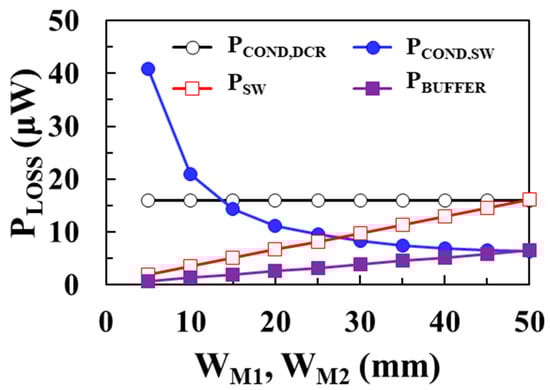
Figure 5.
Modeling results of each loss component according to the width of M1 and M2 switches.
Figure 6 shows the modeling results of each loss component of the boost converter according to the peak inductor current IP using (3)–(6) when VIN = 0.1 V, VOUT = 1 V, ILOAD = 1 mA, WM1 = WM2 = 20 mm, and L = 10 μH. As the peak inductor current increases, conduction loss of the inductor and switches increase and switching loss and buffer loss decrease.
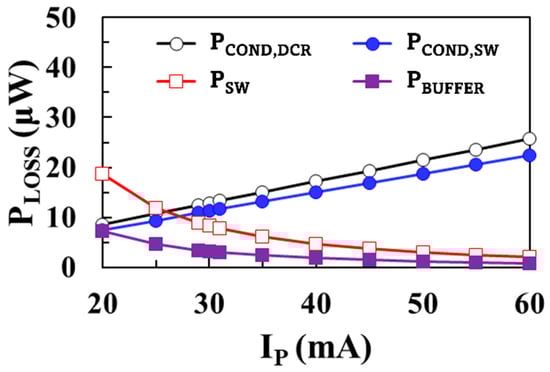
Figure 6.
Modeling results of each loss component according to the peak inductor current.
5. Proposed Efficiency Optimization Design
Figure 7 shows the schematic of the DC-DC boost converter with the control circuits for generating the pulses to drive and control the switches. The low input voltage DC-DC boost converter operates in discontinuous conduction mode (DCM) to obtain higher efficiency at the low input voltage operation of 0.1 V. A pulse width modulation (PWM) scheme-based control system is applied to keep the output voltage constant in the DC-DC boost converter. The PWM scheme-based control method adjusts the output voltage of the converter under different load current conditions by adjusting the duty cycle of the drive signal with a fixed frequency []. The duty cycle of the driving signal to control the NMOS and PMOS switches of a DC-DC converter is proportional to the control voltage, which is the difference between the output voltage of the converter and the reference voltage. The PWM input (VPWM) is used to drive the switch transistor M1 through the buffer. The time delay controlled by the digital gates and CDELAY compensates for the time delay between the switch control signals VN and VP so that transistor M2 turns on quickly enough after transistor M1 turns off. The output of the OR gate drives the gate of the switch transistor M2 through a buffer. Current sensing for switch transistor M2 is performed by a comparator and the comparator’s output signal is used to sense when the current through switch transistor M2 goes to zero.
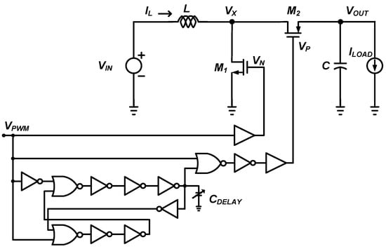
Figure 7.
Schematic of the DC-DC boost converter with the control circuits.
In an RF-DC converter for RF energy harvesting, the output DC voltage varies according to the RF input power. Therefore, the DC-DC boost converter following the RF-DC converter is required to achieve high efficiency over a wide input voltage range. To obtain high efficiency in a wide input voltage range, it is necessary to derive the optimal value of each design parameter to minimize the loss by modeling the loss of the converter according to the input voltage.
Figure 8 shows the modeled total loss (PTOTAL) as a function of inductance L using (7) for input voltages of 0.1 V, 0.2 V, and 0.4 V, respectively, when VOUT = 1 V, ILOAD = 1 mA, WM1 = WM2 = 20 mm, and IP = 30 mA. Figure 9 shows the modeled power conversion efficiency (PCE) as a function of the inductance L using (7) for input voltages of 0.1 V, 0.2 V, and 0.4 V, respectively. As the input voltage increases, the optimum inductance to achieve the minimum total loss increases. At an input voltage of 0.1 V, a maximum efficiency of 96.5% is achieved when L is 6.8 μH. At input voltages of 0.2 V and 0.4 V, maximum efficiencies of 97.7% and 98.5% are achieved when L is 10 μH, respectively.
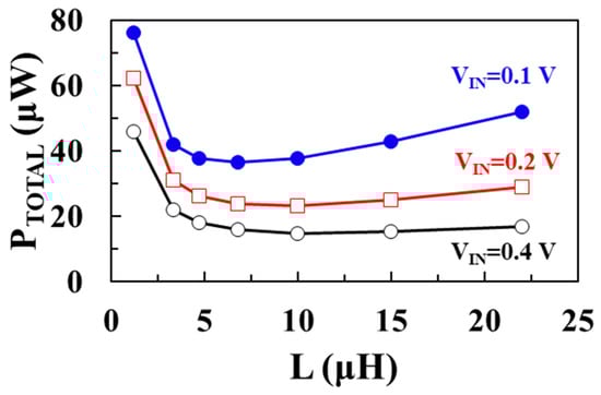
Figure 8.
Modeled total loss according to inductance for different input voltages.
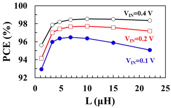
Figure 9.
Modeled PCE according to inductance for different input voltages.
Figure 10 shows the modeled total loss (PTOTAL) as a function of peak inductor current IP using (7) for input voltages of 0.1 V, 0.2 V, and 0.4 V, respectively, when VOUT = 1 V, ILOAD = 1 mA, L = 10 μH, WM1 = WM2 = 20 mm. Figure 11 shows the PCE according to the peak inductor current (IP) for input voltages of 0.1 V, 0.2 V, and 0.4 V, respectively. As the input voltage increases, the optimum peak inductor current to achieve the minimum total loss increases. At an input voltage of 0.1 V, a maximum efficiency of 96.6% is achieved when IP is 29 mA. At an input voltage of 0.2 V, a maximum efficiency of 97.7% is achieved when IP is 31 mA, and at an input voltage of 0.4 V, a maximum efficiency of 98.7% is achieved when IP is 33 mA.
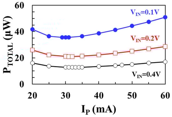
Figure 10.
Modeled total loss according to peak inductor current for different input voltages.
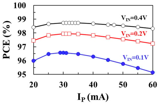
Figure 11.
Modeled PCE according to peak inductor current for different input voltages.
6. Simulation Results and Comparison
In this paper, the DC-DC boost converter has been designed using a 65 nm CMOS technology. To verify the effectiveness of the DC-DC boost converter and to compare it with the proposed model, post-layout simulations with Spectre were carried out. Figure 12 shows the waveforms of the switch control signals VN and VP, internal node voltage VX, output voltage VOUT, and inductor current IL for an input voltage of 0.1 V.
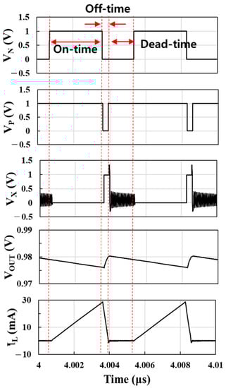
Figure 12.
Waveforms of the switch control signals VN and VP, internal node voltage VX, inductor current IL, and output voltage VOUT for an input voltage of 0.1 V.
VN and VP are the output signals of the control circuit to control the switch on-off of the converter. When VN and VP are high at the same time, the inductor is connected to ground during on time so that IL increases from 0 mA to 29 mA and the load capacitor is discharged by the load current and VOUT decreases. When VN and VP are low at the same time, the inductor is connected to the output during off time and the output capacitor is not only discharged by the constant load current but also charged by the inductor current, so that VOUT increases. Conduction losses mainly occur as current flows during on time and off time. During the dead time when VN is low and VP is high, no current flows through the inductor and, as in the on-time period, the output capacitor is discharged by constant load current and VOUT decreases. Ringing occurs due to the resonance of the inductor and parasitic capacitor during dead time.
Figure 13 shows the total loss of the DC-DC boost converter according to the inductance L for an input voltage of 0.1 V and compares the circuit simulation results with the proposed modeling results when VOUT = 1 V, ILOAD = 1 mA, WM1 = WM2 = 20 mm, and IP = 30 mA. As the inductance decreases, the switching frequency increases and the switching losses of NMOS and PMOS increase. On the other hand, as the inductance increases, the ESR of the inductor increases and conduction loss of the inductor increases. Therefore, there is an optimal inductance value that minimizes the total loss. It shows that the modeled total loss of the boost converter agrees well with the circuit simulation results, with a minimum loss of 36.4 μW achieved for an L of 6.8 μH. Figure 14 shows the PCE of the converter according to L for an input voltage of 0.1 V and compares the circuit simulation results with the proposed modeling results. A maximum efficiency of 96.5% is achieved at an optimum L of 6.8 μH and the proposed model accurately predicts the optimal L value to obtain the maximum PCE.
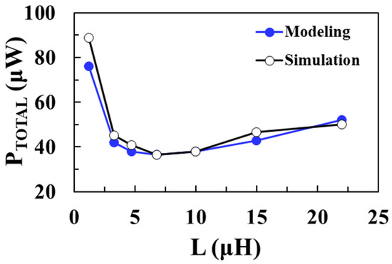
Figure 13.
Total loss according to inductance for an input voltage of 0.1 V and comparison with the modeling results.
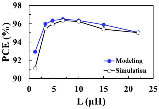
Figure 14.
PCE according to inductance for an input voltage of 0.1 V and comparison with the modeling results.
Figure 15 shows the total loss of the DC-DC boost converter according to the width of M1 and M2 switches for an input voltage of 0.1 V and compares the circuit simulation results with the proposed modeling results when VOUT = 1 V, ILOAD = 1 mA, L = 10 μH, and IP = 30 mA. As the NMOS and PMOS switches’ width decreases, the on resistance increases and the conduction losses of the switches increase. On the other hand, as the switches’ width increases, the capacitances increase and the switching losses of the NMOS and PMOS increase. Therefore, there is an optimal switch width that minimizes the total loss. The modeled total loss agrees well with the circuit simulation results and a minimum loss of 36.3 μW is achieved when the switch width is 20 mm. Figure 16 shows the PCE of the boost converter according to the width of M1 and M2 switches for an input voltage of 0.1 V and compares the circuit simulation results with the proposed modeling results. A maximum efficiency of 96.5% is achieved at an optimum switch width of 20 mm and the proposed model accurately predicts the optimal switch width to obtain the maximum PCE.
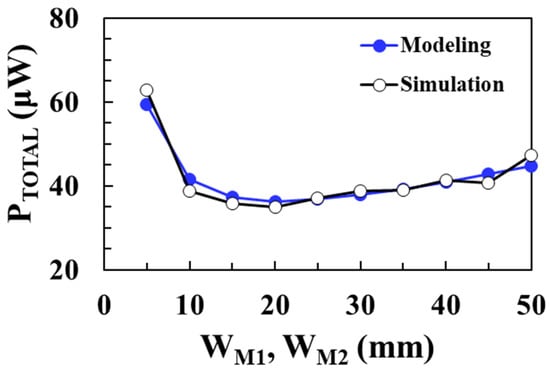
Figure 15.
Total loss according to the switch width for an input voltage of 0.1 V and comparison with the modeling results.
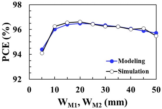
Figure 16.
PCE according to switch width for an input voltage of 0.1 V and comparison with the modeling results.
Figure 17 shows the total loss of the DC-DC boost converter according to the peak inductor current IP for an input voltage of 0.1 V and compares the circuit simulation results with the proposed modeling results when VOUT = 1 V, ILOAD = 1 mA, L = 10 μH, and WM1 = WM2 = 20 mm. As the peak inductor current decreases, the switching frequency increases and the switching losses of the NMOS and PMOS increase. On the other hand, as the peak inductor current increases, conduction losses in the switches and inductor increase. Therefore, there is an optimal peak inductor current that minimizes total losses. The modeled total loss agrees well with the circuit simulation results, with a minimum loss of 35.6 μW achieved at an IP of 29 mA. Figure 18 shows the PCE of the boost converter according to the peak inductor current IP for an input voltage of 0.1 V and compares the circuit simulation results with the proposed modeling results. A maximum efficiency of 96.6% is achieved at an optimum IP of 29 mA and the proposed model accurately predicts the optimal IP to obtain the maximum PCE.
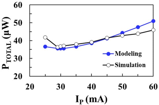
Figure 17.
Total loss according to the peak inductor current for an input voltage of 0.1 V and comparison with the modeling results.
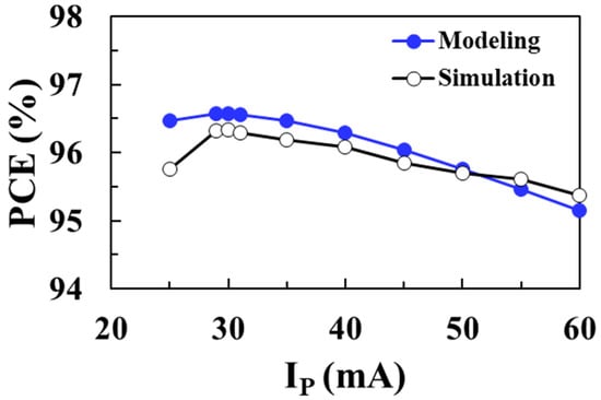
Figure 18.
PCE according to the peak inductor current for an input voltage of 0.1 V and comparison with the modeling results.
Figure 19 shows the PCE of the converter according to the input voltage and compares the circuit simulation results with the proposed modeling results when VOUT = 1 V, ILOAD = 1 mA, and WM1 = WM2 = 20 mm. Based on the proposed optimal design methodology to achieve the maximum PCE, the optimal values of inductance and peak inductor current are designed differently according to the input voltage. As the input voltage increases, the optimum inductance and peak inductor current to achieve the minimum total loss increase. At an input voltage of 0.1 V, a maximum PCE of 96.5% is achieved when L is 6.8 μH and IP is 29 mA. On the other hand, at an input voltage of 0.4 V, a maximum PCE of 98.4% is achieved when L is 10 μH and IP is 33 mA. The PCE modeling results achieved from the proposed efficiency optimization design method based on loss analysis and modeling are in good agreement with circuit simulation results over a wide input voltage range. By deriving the optimal design parameters including inductance and peak inductor current for different input voltages, the maximum PCE is achieved over a wide input voltage range.
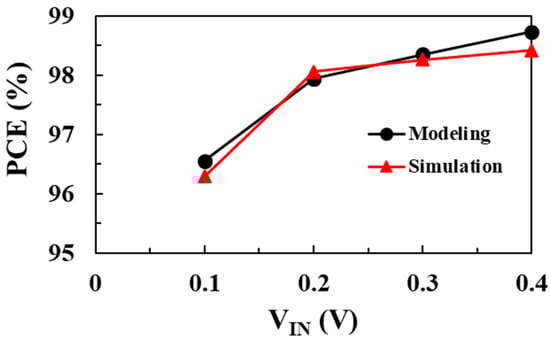
Figure 19.
PCE according to input voltage comparison with the modeling results.
Table 1 summarizes the performance of this work and compares with the state-of-the-art DC-DC boost converters for energy harvesting applications. The proposed boost converter for RF energy harvesting operates over a wide input voltage range and achieves a PCE of 96.5% at a low input voltage of 0.1 V and the highest peak efficiency of 98.4% at an input voltage of 0.4 V.

Table 1.
Performance summary and comparison.
7. Conclusions
In this paper, an optimization design methodology for a high-efficiency DC-DC boost converter is proposed based on loss analysis and modeling of an inductor-based DC-DC boost converter. In the proposed efficiency optimization design methodology of the DC-DC boost converter, each loss component of the inductor-based DC-DC boost converter is analyzed and the loss modeling result according to the design parameters is presented. Based on the loss analysis and modeling, optimum design parameters including inductance and peak inductor current are obtained to achieve the maximum PCE by minimizing the total loss according to different input voltages in a wide input voltage range. The modeled total losses agree well with the circuit simulation results and the proposed loss modeling results accurately predict the optimum design parameters to obtain the maximum PCE. The designed DC-DC boost converter achieves a power conversion efficiency of 96.5% at a low input voltage of 0.1 V and a peak efficiency of 98.4% at an input voltage of 0.4 V. To further improve the power conversion efficiency of the DC-DC boost converter for RF energy harvesting, not only the efficiency optimization design method of the proposed converter core circuit but also the efficiency optimization design method of the converter switch control circuit is required; therefore, further research on this is needed in the future.
Author Contributions
Conceptualization, I.K.; methodology, I.K.; software, J.K.; validation, J.K. and I.K.; formal analysis, J.K. and I.K.; investigation, J.K.; resources, I.K.; data curation, J.K.; writing—original draft preparation, J.K. and I.K.; writing—review and editing, I.K.; visualization, J.K.; supervision, I.K.; project administration, I.K.; funding acquisition, I.K. All authors have read and agreed to the published version of the manuscript.
Funding
This work was supported by the National Research Foundation of Korea (NRF) grant funded by the Korea government (MSIT) (No. 2021R1A2C1010613).
Institutional Review Board Statement
Not applicable.
Informed Consent Statement
Not applicable.
Data Availability Statement
Not applicable.
Acknowledgments
The chip fabrication and EDA tool were supported by the IC Design Education Center (IDEC), Korea.
Conflicts of Interest
The authors declare no conflict of interest.
Abbreviations
| Symbol/Notation | Description |
| fSW | switching frequency |
| IP | peak inductor current |
| ILOAD | load current |
| L | inductance |
| WM1 and WM2 | width of the switches M1 and M2 |
| PCE | power conversion efficiency |
| PTOTAL | total loss of the converter |
| PCOND,DCR | conduction loss due to the resistance of inductor |
| PCOND,SW | conduction loss due to the switches |
| PSW | switching loss of the NMOS and PMOS switches |
| PBUFFER | switching loss of the buffer stages |
References
- Gorlatova, M.; Sarik, J.; Grebla, G.; Cong, M.; Kymissis, I.; Zussman, G. Movers and shakers: Kinetic energy harvesting for the Internet of things. IEEE J. Sel. Areas Commun. 2015, 33, 1624–1639. [Google Scholar] [CrossRef]
- Alzahrani, B.; Ejaz, W. Resource management for cognitive IoT systems with RF energy harvesting in smart cities. IEEE Access 2018, 6, 62717–62727. [Google Scholar] [CrossRef]
- Ercan, A.Ö.; Sunay, M.O.; Akyildiz, I.F. RF energy harvesting and transfer for spectrum sharing cellular IoT communications in 5G systems. IEEE Trans. Mob. Comput. 2018, 17, 1680–1694. [Google Scholar] [CrossRef]
- Mouapi, A. Radiofrequency Energy Harvesting Systems for Internet of Things Applications: A Comprehensive Overview of Design Issues. Sensors 2022, 22, 8088. [Google Scholar] [CrossRef] [PubMed]
- Churchill, K.K.P.; Ramiah, H.; Chong, G.; Chen, Y.; Mak, P.-I.; Martins, R.P. A Fully-Integrated Ambient RF Energy Harvesting System with 423-μW Output Power. Sensors 2022, 22, 4415. [Google Scholar] [CrossRef]
- Ibrahim, H.H.; Singh, M.J.; Al-Bawri, S.S.; Ibrahim, S.K.; Islam, M.T.; Alzamil, A.; Islam, M.S. Radio Frequency Energy Harvesting Technologies: A Comprehensive Review on Designing, Methodologies, and Potential Applications. Sensors 2022, 22, 4144. [Google Scholar] [CrossRef]
- Sherazi, H.H.R.; Zorbas, D.; O’Flynn, B. A Comprehensive Survey on RF Energy Harvesting: Applications and Performance Determinants. Sensors 2022, 22, 2990. [Google Scholar] [CrossRef]
- Benkalfate, C.; Ouslimani, A.; Kasbari, A.-E.; Feham, M. A New RF Energy Harvesting System Based on Two Architectures to Enhance the DC Output Voltage for WSN Feeding. Sensors 2022, 22, 3576. [Google Scholar] [CrossRef]
- Churchill, K.K.P.; Chong, G.; Ramiah, H.; Ahmad, M.Y.; Rajendran, J. Low-Voltage Capacitive-Based Step-Up DC-DC Converters for RF Energy Harvesting System: A Review. IEEE Access 2020, 8, 186393–186407. [Google Scholar] [CrossRef]
- The, Y.K.; Mok, P.K.T. Design of transformer-based boost converter for high internal resistance energy harvesting sources with 21 mV self-startup voltage and 74% power efficiency. IEEE J. Solid-State Circuits 2014, 49, 2694–2703. [Google Scholar]
- Shih, Y.-C.; Otis, B.P. An inductorless DC–DC converter for energy harvesting with a 1.2-μW bandgap-referenced output controller. IEEE Trans. Circuits Syst. II Exp. Briefs 2011, 58, 832–836. [Google Scholar]
- Donno, D.D.; Catarinucci, L.; Tarricone, L. An UHF RFID energy-harvesting system enhanced by a DC-DC charge pump in silicon-on-insulator technology. IEEE Microw. Wirel. Compon. Lett. 2013, 23, 315–317. [Google Scholar] [CrossRef]
- Kim, J.; Mok, P.K.T.; Kim, C. A 0.15 V Input Energy Harvesting Charge Pump with Dynamic Body Biasing and Adaptive Dead-Time for Efficiency Improvement. IEEE J. Solid-State Circuits 2015, 50, 414–425. [Google Scholar] [CrossRef]
- Potocny, M.; Kovac, M.; Arbet, D.; Sovcik, M.; Nagy, L.; Stopjakova, V.; Ravasz, R. Low-Voltage DC-DC Converter for IoT and On-Chip Energy Harvester Applications. Sensors 2021, 21, 5721. [Google Scholar] [CrossRef]
- Newell, D.; Duffy, M. Review of Power Conversion and Energy Management for Low-Power, Low-Voltage Energy Harvesting Powered Wireless Sensors. IEEE Trans. Power Electron. 2019, 34, 9794–9805. [Google Scholar] [CrossRef]
- Weng, P.-S.; Tang, H.-Y.; Ku, P.-C.; Lu, L.-H. 50 mV-input batteryless boost converter for thermal energy harvesting. IEEE J. Solid-State Circuits 2013, 48, 1031–1041. [Google Scholar] [CrossRef]
- Chen, P.-H.; Fan, P.M.-Y. An 83.4% peak efficiency single inductor multiple-output based adaptive gate biasing DC-DC converter for thermoelectric energy harvesting. IEEE Trans. Circuits Syst. I Reg. Pap. 2015, 62, 405–412. [Google Scholar] [CrossRef]
- Shrivastava, A.; Roberts, N.E.; Calhoun, B.H. A 10 mV-Input Boost Converter with Inductor Peak Current Control and Zero Detection for Thermoelectric and Solar Energy Harvesting with 220 mV Cold-Start and 14.5 dBm, 915 MHz RF Kick-Start. IEEE J. Solid-State Circuits 2015, 50, 1820–1832. [Google Scholar] [CrossRef]
- Bandyopadhyay, S.; Mercier, P.P.; Lysaght, A.C.; Stankovic, K.M. A 1.1 nW Energy Harvesting System with 544 pW Quiescent Power for Next-Generation Implants. IEEE J. Solid-State Circuits 2014, 49, 2812–2824. [Google Scholar] [CrossRef]
- Lim, B.M.; Seo, J.I.; Lee, S.G. A Colpitts Oscillator-Based Self-Starting Boost Converter for Thermoelectric Energy Harvesting with 40-mV Startup Voltage and 75% Maximum Efficiency. IEEE J. Solid-State Circuits 2018, 53, 3293–3302. [Google Scholar] [CrossRef]
- Liu, C.W.; Lee, H.H.; Chen, P.H. Dual-Source Energy-Harvesting Interface with Cycle-by-Cycle Source Tracking and Adaptive Peak-Inductor Current Control. IEEE J. Solid-State Circuits 2018, 53, 2741–2750. [Google Scholar] [CrossRef]
- Katic, J.; Rodriguez, S.; Rusu, A. A Dual-Output Thermoelectric Energy Harvesting Interface with 86.6% Peak Efficiency at 30 μW and Total Control Power of 160 nW. IEEE J. Solid-State Circuits 2016, 51, 1928–1937. [Google Scholar] [CrossRef]
- Mu, J.; Liu, L. A 12 mV Input, 90.8% Peak Efficiency CRM Boost Converter with a Sub-Threshold Startup Voltage for TEG Energy Harvesting. IEEE Trans. Circuits Syst. I Reg. Pap. 2018, 65, 2631–2640. [Google Scholar] [CrossRef]
- Wang, J.; Jiang, Y.; Dijkhuis, J.; Dolmans, G.; Gao, H.; Baltus, P. A 900 MHz RF energy harvesting system in 40 nm CMOS technology with efficiency peaking at 47% and higher than 30% over a 22 dB wide input power range. In Proceedings of the 2017 IEEE European Solid State Circuits Conference (ESSCIRC), Leuven, Belgium, 11–14 September 2017. [Google Scholar]
- Sadagopan, K.R.; Kang, J.; Ramadass, Y.; Natarajan, A. A cm-Scale 2.4-GHz Wireless Energy Harvester with Nanowatt Boost Converter and Antenna-Rectifier Resonance for WiFi Powering of Sensor Nodes. IEEE J. Solid-State Circuits 2018, 53, 3396–3406. [Google Scholar] [CrossRef]
- Saini, G.; Somappa, L.; Baghini, M.S. A 500 nW to 1 mW input power inductive boost converter with MPPT for RF energy harvesting system. IEEE J. Emerg. Sel. Top. Power Electron. 2021, 9, 5261–5271. [Google Scholar] [CrossRef]
Publisher’s Note: MDPI stays neutral with regard to jurisdictional claims in published maps and institutional affiliations. |
© 2022 by the authors. Licensee MDPI, Basel, Switzerland. This article is an open access article distributed under the terms and conditions of the Creative Commons Attribution (CC BY) license (https://creativecommons.org/licenses/by/4.0/).