
Fast Constant-Time Modular Inversion over

 , , ,
, , ,  and
and
Abstract
:1. Introduction
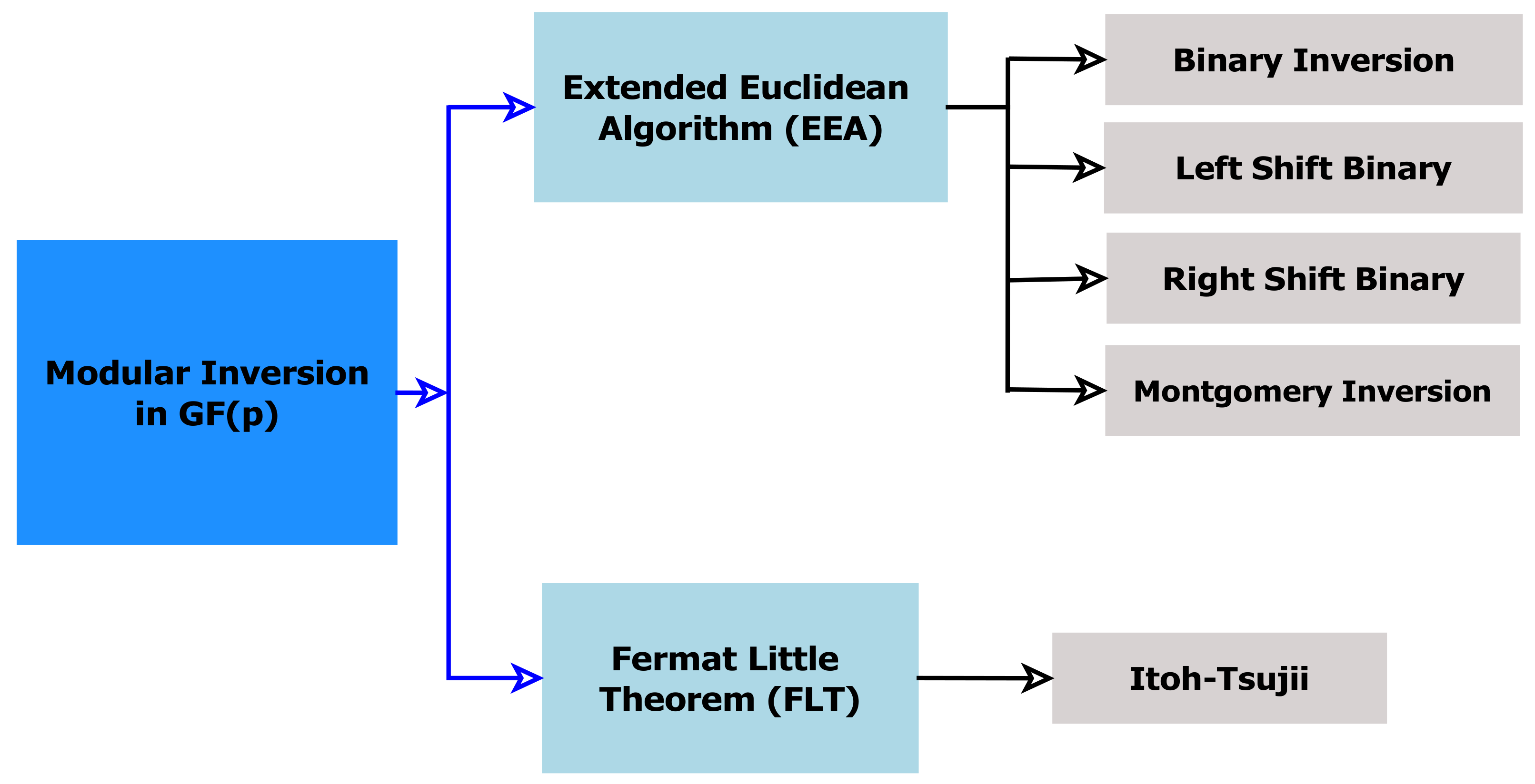
2. Related Works
3. BEE Algorithm
| Algorithm 1: Pseudo-code of the BEE algorithm. |
 |
4. Constant-Time Modular Inversion
- The same amount of time is always taken to compute an iteration. In constant time, this requires computing all four branches of Algorithm 1 and selecting the appropriate values. As a result, the computed time of each iteration is independent of the branch taken; however, it may be increased to (at most) that of the computation of the sum of all the branches.
- The algorithm always has the same number of iterations. As a result, the worst-case number of ‘K’ iterations should always be calculated. It can be achieved by determining when Algorithm 1 terminates (when we reach v = 1 or u = 1).
- The shift-by-one function denoted by : this function shifts x by one position to the left and stores the result in z.
- The subtraction and addition functions are denoted respectively by sub (z, x, y) and add (z, x, y)) computing z x − y and z x + y. Those two functions are computed by the adder/subtractor G-KSA/S which is discussed in the next section.
- The function are used respectively to save the values of u and if u is even ( = 0, RAM active 0), and the values of v and if v is even ( = 0, RAM active 0). As the LUT area is 2n, we need four look-up tables to memorize u, , v, and .
- The comparison function is denoted by comp (u, v). This function is used to compare ‘u’ and ‘v’ values.
- The function denoted ()
- The occurrence function is denoted by occur (RAM, u, 1, i), which means the first occurrence of 1 in RAM of u indicates the corresponding i, then:
| Algorithm 2: Pseudo-code of the proposed modified BEE algorithm | |
| 1. Input:p and a ∈ 2. Output mod p 3. Define; u = a; v = p 4. Define; x1 = 1; x2 = 0 5. Define; p’ = Rshift(p,1) | |
| Inversion steps | |
| 6. for; i++) { | |
|
6.1. 6.2. 6.3. add(, ,(p’ (0)) 6.4. (u(0)) | # u # # |
|
6.5. 6.6. 6.7. add(, ,(p’ (0)) 6.8. (v(0)) | # v # # |
|
6.9. comp(u,v) 6.10. 6.11. | # If u v # u # |
|
6.12. () 6.13. 6.14. 6.15. ( | # v # |
|
6.16. occur(RAM, u, 1,i) 6.17. occur(RAM, v, 1,j) 6.18. return (i,j,x) 7. } | # Return mod p if u equal 1 # Return mod p if v equal 1 |
- The initial step: ‘a’ and ‘p’ are assigned to ‘u’ and ‘v’, respectively. Moreover, in this step, ‘1′ and ‘0′ are assigned to x1 and x2, respectively.
- Updating step: u, v, x1, and x2 values are updated by three different operations: add, sub, left shift (), , and . The updating process is executed throughout the entire loop ((1 < i < k) execution time) and managed by two signals: sel1 and sel2. The new (u, v, x1, and x2) values are assigned according to sel1 and sel2, and these control signals are updated in step 12.9 during each iteration of the “for loop”.
- Return ‘b’ after k iterations.
5. MBEEA Implementation
- Controller unit: This generates control signals for all the MBEEA architecture units and the data flow in the inverter design, and the movement of data between the adder-subtractor units, the memory units, the comparator unit, and the occurrence units.
- Adder/Subtractor (G-KSA/S): This performs the addition or the subtraction of two values according to the controller decision.
- Memory unit (MU): The main purpose of this unit is to store different parameters such as u, v, x1, and x2, and their intermediate results. It constitutes of four blocks of RAM (RAMu, RAMv, RAMx1, and RAMx2) and multiplexers that are used to read operands (u, v, x1, and x2) from the MU using the corresponding control signals.
- Comp unit: This is a comparator between u and v. It has a 3-bit output to indicate whether u > v or u < v or u = v.
- Occur unit: This searches for u = 1 occurrence. Return x 1 mod p if u equal 1. Otherwise, if v is 1, return x2 mod p.

5.1. Kogge–Stone Adder/Subtractor Unit: Design and Implementation
| Algorithm 3: G-KSA/S algorithm |
|
Input: (A,B) Define: n; n = bit length of p Pre-computed:S = [1,2,4,8,16,32,64,128], j 1, k 1 Output: ( Preprocessing Step 1: For (i = 0; i to n − 1; i++) { C(i) := B(i); }; Step 2: For (i = 0; i n − 1; i++) { 2.1: := A(i)C(i); 2.2: := A(i)C(i); }; Parallel Prefix Network Step 3: For (i = 0; ij-1; i++) { 3.1 := , 3.2 := }; Step 4: For (i = 0; ij-1){ 4.1: := (; 4.2: := (; }; k + +;j := S[k-1], T := m − 1; IF(T > 0) go to step 3 ELSE go to step 5 Step 5: For (i = 0; i n-1; i++) { 5.1: C(i) := (i)((i)); }; Post-processing Step 6: 6.1:sum(0) = (0) ; 6.2: For (i = 1; in-1; i++){ 6.2.1: sum(i) = (i)C(i − 1); }; Step 7: = C(N − 1); Return Sum, |
5.2. The Modular Reduction
- General module forms (i.e., Barrett and Montgomery algorithms), which are slower and present an expansive part of the arithmetic operation.
- Based on the LUT method (which is based on pre-computed values); however, this requires a large amount of memory.
- Modulo form of prime numbers, such as pseudo-Mersenne numbers. Their special form makes them appropriate for modular reduction. The pseudo-Mersenne prime number p is presented with the special form: p = – c, where = n (n represents the security level) and ‘c’ is a positive integer that is relatively small compared to the modulus. An integer can be represented in radix- by spilling z up into a lower part and a higher part + . Then, using the fact that ≡ c mod p, we have + ≡ c + mod p where 0 ≤ c + < (c + 1). Hence, a multiplication of by the constant c is needed and the final result is obtained after the addition of . For the three values of n (128, 192, and 256), the resulting primes satisfy p ≡ 3 (mod 4).
5.3. Controller Unit
6. Results and Performance Analysis
6.1. G-KSA/S Implementation Results

| Designs | Platform | n = Bit Length of p | Area (Slices) | Delay (ns) | ADP (10−9) | Gain % |
|---|---|---|---|---|---|---|
| [34] | Spartan-3E | 8 | 83 | 5.776 | 479.408 | |
| G-KSA/S | Spartan-3E | 47 | 3.6 | 169.2 | 74.71% | |
| [34] | Spartan-3E | 16 | 166 | 10.85 | 1801.1 | |
| G-KSA/S | Spartan-3E | 98 | 7.3 | 715.4 | 61.28% | |
| [34] | Spartan-3E | 32 | 332 | 20.56 | 6825.92 | |
| G-KSA/S | Spartan-3E | 174 | 12.3 | 2140.2 | 68.65% | |
| [35] | Virtex-5 | 64 | 449 | 30.5 | 13,694.5 | |
| G-KSA/S | Virtex-5 | 289 | 27.9 | 8063.1 | 41.13% | |
| [35] | Virtex-5 | 128 | 1111 | 57.3 | 63,660.3 | |
| G-KSA/S | Virtex-5 | 641 | 64.4 | 41,280.4 | 35.16% | |
| [35] | Virtex-5 | 256 | 1345 | 106.7 | 143,511.5 | |
| G-KSA/S | Virtex-5 | 737 | 139 | 102,443 | 28.62% |
6.2. MBEEA Implementation Results
| Design | n = Bit Length of p | Freq. (MHz) | Area (Slices) | Latency (μs) |
|---|---|---|---|---|
| 8 | 530 | 545 | 0.179 | |
| 16 | 480 | 770 | 0.27 | |
| 32 | 420 | 1060 | 0.346 | |
| 64 | 380 | 1237 | 0.428 | |
| 128 | 310 | 1532 | 0.851 | |
| 256 | 250 | 2035 | 1.24 |
7. Conclusions
Author Contributions
Funding
Institutional Review Board Statement
Informed Consent Statement
Conflicts of Interest
References
- Lee, S.; Huh, J.-H. An effective security measures for nuclear power plant using big data analysis approach. J. Supercomput. 2019, 75, 4267–4294. [Google Scholar] [CrossRef]
- Kim, S.-K.; Kim, U.-M.; Huh, J.-H. A Study on Improvement of Blockchain Application to Overcome Vulnerability of IoT Multiplatform Security. Energies 2019, 12, 402. [Google Scholar] [CrossRef] [Green Version]
- Miller, V.-S. Use of elliptic curves in cryptography. In Advances in Cryptology—CRYPTO ’85 Proceedings. CRYPTO 1985; Lecture Notes in Computer Science; Springer, Inc.: New York, NY, USA, 1986; pp. 417–426. [Google Scholar]
- Islam, T.; Youki, R.-A.; Chowdhury, B.-R.; Hasan, A.-S.M.T. An ECC Based Secure Communication Protocol for Resource Constraints IoT Devices in Smart Home. In Proceedings of the International Conference on Big Data, IoT, and Machine Learning; Lecture Notes on Data Engineering and Communications Technologies; Arefin, M.S., Kaiser, M.S., Bandyopadhyay, A., Ahad, M.A.R., Ray, K., Eds.; Springer: Singapore, 2022; Volume 95. [Google Scholar]
- Lohachab, K.A. ECC based inter-device authentication and authorization scheme using MQTT for IoT networks. J. Inf. Secur. Appl. 2019, 46, 1–12. [Google Scholar] [CrossRef]
- Marin, L.; Pawlowski, M.-P.; Jara, A. Optimized ECC Implementation for Secure Communication between Heterogeneous IoT Devices. Sensors 2015, 15, 21478–21499. [Google Scholar] [CrossRef] [Green Version]
- Varchola, M.; Drutarovsky, M.; Repka, M.; Zajac, P. Side-channel attack on multi-precision multiplier used in protected ecdsa implementation. In Proceedings of the 2015 International Conference on ReConFigurable Computing and FPGAs (ReConFig), Riviera Maya, Mexico, 7–9 December 2015; pp. 1–6. [Google Scholar]
- Fan, J.; Verbauwhede, I. An updated survey on secure ECC implementations: Attacks, countermeasures and cost. In Cryptography and Security: From Theory to Applications; Springer: Berlin/Heidelberg, Germany, 2012; pp. 265–282. [Google Scholar]
- Rafik, M.-B.-O.; Mohammed, F. The impact of ecc’s scalar multiplication on wireless sensor networks. In Proceedings of the 2013 11th International Symposium on Programming and Systems (ISPS), Algiers, Algeria, 22–24 April 2013; pp. 17–23. [Google Scholar]
- Ghosh, S.; Mukhopadhyay, D.; Roychowdhury, D. Petrel: Power and timing attack resistant elliptic curve scalar multiplier based on programmable GF(p) arithmetic unit. IEEE Trans. Circuits Syst. I Regul. Pap. 2011, 58, 1798–1812. [Google Scholar] [CrossRef]
- Kocher, P.C. Timing Attacks on Implementations of Diffie-Hellman, RSA, DSS, and Other Systems. In Advances in Cryptology—CRYPTO’96; Lecture Notes in Computer Science; Koblitz, N., Ed.; Springer: Berlin/Heidelberg, Germany, 1996; Volume 1109. [Google Scholar]
- Shanmugham, S.-R.; Paramasivam, S. Survey on power analysis attacks and its impact on intelligent sensor networks. IET Wirel. Sens. Syst. 2018, 8, 295–304. [Google Scholar] [CrossRef] [Green Version]
- Moon, J.; Junga, I.-Y.; Park, J.-H. IoT application protection against power analysis attack. Comput. Electr. Eng. 2018, 67, 566–578. [Google Scholar] [CrossRef]
- Arpaia, P.; Bonavolontà, F.; Cioffi, A.; Moccaldi, N. Reproducibility Enhancement by Optimized Power Analysis Attacks in Vulnerability Assessment of IoT Transducers. IEEE Trans. Instrum. Meas. 2021, 70, 1–8. [Google Scholar] [CrossRef]
- Dao, B.A.; Hoang, T.T.; Le, A.T.; Tsukamoto, A.; Suzaki, K.; Pham, C.K. Exploiting the Back-Gate Biasing Technique as a Countermeasure Against Power Analysis Attacks. IEEE Access 2021, 9, 24768–24786. [Google Scholar] [CrossRef]
- Dubeuf, J.; Hely, D.; Beroulle, V. ECDSA Passive Attacks, Leakage Sources, and Common Design Mistakes. ACM Trans. Des. Autom. Electron. Syst. 2016, 21, 1–24. [Google Scholar] [CrossRef]
- Genkin, D.; Pachmanov, L.; Pipman, I.; Tromer, E.; Yarom, Y. ECDSA Key Extraction from Mobile Devices via Nonintrusive Physical Side Channels. In Proceedings of the ACM SIGSAC Conference on Computer and Communications Security, Vienna, Austria, 24–28 October 2016; pp. 1626–1638. [Google Scholar]
- Zhang, K.; Xu, S.; Gu, D.; Gu, H.; Liu, J.; Guo, Z.; Liu, R.; Liu, L.; Hu, X. Practical Partial-Nonce-Exposure Attack on ECC Algorithm. In Proceedings of the 13th International Conference on Computational Intelligence and Security (CIS), Hong Kong, China, 15–18 December 2017. [Google Scholar]
- Wunan, W.; Hao, C.; Jun, C. The Attack Case of ECDSA on Blockchain Based on Improved Simple Power Analysis. In Artificial Intelligence and Security. ICAIS 2019; Lecture Notes in Computer Science; Springer: Cham, Switzerland, 2019; Volume 11635. [Google Scholar]
- Thibault, J.-P.; O’Flynn, C.; Dewar, A. Ark of the ECC: An Open-Source ECDSA Power Analysis Attack on an FPGA Based Curve P-256 Implementation. Cryptology ePrint Archive: Report 2021/1520. 2021. Available online: https://eprint.iacr.org/2021/1520 (accessed on 25 January 2022).
- Sghaier, A.; Zeghid, M.; Massoud, C.; Mahchout, M. Design and Implementation of Low Area/Power Elliptic Curve Digital Signature Hardware Core. Electronics 2017, 6, 46. [Google Scholar] [CrossRef] [Green Version]
- Choi, P.; Lee, M.K.; Kong, J.T.; Kim, D.K. Efficient Design and Performance Analysis of a Hardware Right-shift Binary Modular Inversion Algorithm in GF(p). J. Semicond. Technol. Sci. 2017, 17, 425–437. [Google Scholar]
- Alhazmi, B.; Gebali, F. Fast Large Integer Modular Addition in GF(p) Using Novel Attribute-Based Representation. IEEE Access 2019, 7, 58704–58719. [Google Scholar] [CrossRef]
- Janwadkar, S.; Dhavse, R. Qualitative and Quantitative Analysis of Parallel-Prefix Adders. In Advances in VLSI and Embedded Systems; Lecture Notes in Electrical Engineering; Patel, Z., Gupta, S., Kumar, Y.B.N., Eds.; Springer: Singapore, 2020; Volume 676. [Google Scholar]
- Bos, J.-W. Constant time modular inversion. J. Cryptogr. Eng. 2014, 4, 275–281. [Google Scholar] [CrossRef]
- Liu, Z.; Großschädl, J.; Li, L.; Xu, Q. Energy-efficient elliptic curve cryptography for MSP430-based wireless sensor nodes. In Proceedings of the 21st Australasian Conference on Information Security and Privacy, Melbourne, Australia, 4–6 July 2016; Springer: Cham, Switzerland, 2016; Volume 9722, pp. 94–112. [Google Scholar]
- Xu, S.; Gu, H.; Wang, L.; Guo, Z.; Liu, J.; Lu, X.; Gu, D. Efficient and Constant Time Modular Inversions Over Prime Fields. In Proceedings of the 13th International Conference on Computational Intelligence and Security (CIS), Hong Kong, China, 15–18 December 2017; pp. 524–528. [Google Scholar]
- Aldaya, A.C.; Márquez, R.C.; Sarmiento, A.-J.C.; Sánchez-Solano, S. Side-channel analysis of the modular inversion step in the RSA key generation algorithm. Int. J. Circuit Theory Appl. 2017, 45, 199–213. [Google Scholar] [CrossRef] [Green Version]
- Savaş, E.; Koç, Ç.K. Montgomery inversion. J. Cryptogr. Eng. 2018, 8, 201–210. [Google Scholar] [CrossRef]
- Bernstein, D.-J.; Yang, B.-Y. Fast constant-time gcd computation and modular inversion. IACR Trans. Cryptogr. Hardw. Embed. Syst. 2019, 340–398. [Google Scholar] [CrossRef]
- Awaludin, A.-M.; Larasati, H.-T.; Kim, H. High-Speed and Unified ECC Processor for Generic Weierstrass Curves over GF(p) on FPGA. Sensors 2021, 21, 1451. [Google Scholar] [CrossRef]
- Sarna, S.; Czerwinski, R. RSA and ECC universal, constant time modular inversion. In Proceedings of the AIP Conference Proceedings, Crete, Greece, 29 April–3 May 2020; Volume 2343. [Google Scholar] [CrossRef]
- Aldaya, A.-C.; Sarmiento, A.-J.C.; Sánchez-Solano, S. Spa vulnerabilities of the binary extended Euclidean algorithm. J. Cryptogr. Eng. 2017, 7, 273–285. [Google Scholar] [CrossRef]
- Rajnish, D.; Jitendra, J. An Efficient Processing by using Kogge-Stone High-Speed Addition Technique. Int. J. Comput. Appl. 2015, 131, 21–23. [Google Scholar]
- Vitoroulis, K.; Al-Khalili, A.-J. Performance of Parallel Prefix Adders implemented with FPGA technology. In Proceedings of the 2007 IEEE Northeast Workshop on Circuits and Systems, Montreal, QC, Canada, 5–8 August 2007. [Google Scholar] [CrossRef]
- Hossain, M.-S.; Kong, Y. High-Performance FPGA Implementation of Modular Inversion over F256 for Elliptic Curve Cryptography. In Proceedings of the 2015 IEEE international conference on Data Science and Data Intensive Systems, Sydney, NSW, Australia, 11–13 December 2015; pp. 169–174. [Google Scholar] [CrossRef]
- Hossain, M.-S.; Kong, Y.; Saeedi, E.; Vayalil, N.C. High-performance elliptic curve cryptography processor over NIST prime fields. IET Comput. Digit. Tech. 2016, 11, 33–42. [Google Scholar] [CrossRef]
- Javeed, K.; Wang, X. Low latency flexible FPGA implementation of point multiplication on elliptic curves over GF (p). Int. J. Circuit Theory Appl. 2017, 45, 214–228. [Google Scholar] [CrossRef]
- Javeed, K.; Wang, X.; Scott, M. High-performance hardware support for elliptic curve cryptography over general prime field. Microprocess. Microsyst. 2017, 51, 331–342. [Google Scholar] [CrossRef]
- Mrabet, A.; El-Mrabet, N.; Bouallegue, B.; Mesnager, S.; Machhout, M. An efficient and scalable modular inversion/division for public-key cryptosystems. In Proceedings of the 2017 International Conference on Engineering & MIS (ICEMIS), Monastir, Tunisia, 8–10 May 2017; pp. 1–6. [Google Scholar] [CrossRef]
- Kudithi, T.; Sakthivel, R. High-performance ECC processor architecture design for IoT security applications. J. Supercomput. 2019, 75, 447–474. [Google Scholar] [CrossRef]
- Liu, Z.; Liu, D.; Zou, X. An efficient and flexible hardware implementation of the dual field elliptic curve cryptographic processor. IEEE Trans. Ind. Electron. 2017, 64, 2353–2362. [Google Scholar] [CrossRef]
- Lee, J.W.; Chung, S.C.; Chang, H.-C.; Lee, C.Y. Efficient power analysis resistant dual field elliptic curve cryptographic processor using heterogeneous dual processing element architecture. IEEE Trans. Very Large Scale Integr. (VLSI) 2014, 22, 49–61. [Google Scholar] [CrossRef]
- Vliegen, J.; Mentens, N.; Genoe, J.; Braeken, A.; Kubera, S.; Touha, A.; Verbauwhede, I. A compact FPGA based architecture for elliptic curve cryptography over prime fields. In Proceedings of the ASAP 2010—21st IEEE International Conference on Application-Specific Systems, Architectures and Processors, Rennes, France, 7–9 July 2010; pp. 313–316. [Google Scholar] [CrossRef] [Green Version]
- McIvor, C.J.; McLoone, M.; McCanny, J.V. Hardware elliptic curve cryptographic processor over GF(p). IEEE Trans. Circuits Syst. I Regul. Pap. 2006, 53, 1946–1957. [Google Scholar] [CrossRef]
- Daly, A.; Marnane, W.; Kerins, T.; Popovici, E. An FPGA Implementation of a GF(p) ALU for encryption processors. Microprocess. Microsyst. 2004, 28, 253–260. [Google Scholar] [CrossRef]


| FLT | EEA | BEEA |
|---|---|---|
|
|
|
| n | m | S |
|---|---|---|
| 4 | 2 | 1,2 |
| 8 | 3 | 1,2,4 |
| 16 | 4 | 1,2,4,8 |
| 32 | 5 | 1,2,4,8,16 |
| 64 | 6 | 1,2,4,3,16,32 |
| 128 | 7 | 1,2,4,3,16,32,64 |
| 256 | 8 | 1,2,4,3,16,32,64,128 |
| Ref. | FPGA Device | Freq (MHz) | Time (μs) | Area (Slices) | ADP (×10−9) |
|---|---|---|---|---|---|
| [36] | Virtex-7 | 146.23 | 2.329 | 1480 | 3.44 |
| [37] | Kintex 7 | 142.38 | 2.33 | 1480 | 3.45 |
| [38] | Virtex-6 | 151 | 3.39 | 1190 | 4.04 |
| [39] | Virtex-6 | 146 | 3.52 | 1340 | 4.72 |
| [40] | Virtex-5 | 129 | 7.937 | 592 | 4.7 |
| [41] | Virtex-7 | 138.3 | 2.45 | 1577 | 3.87 |
| [42] | Virtex-II | 55.70 | 6.2 | 5863 | 36.35 |
| [43] | Virtex-II | 37 | 4.98 | 9213 | 45.88 |
| [44] | Virtex-II | 68.17 | 11.60 | 2085 | 24.19 |
| [10] | Virtex-II | 34 | 14.6 | 9146 | 133.53 |
| [45] | Virtex-II | 40.68 | 15.22 | 14,844 | 225.26 |
| [46] | Virtex-II | 50 | 6.4 | 5477 | 35 |
| MBEEA | Virtex-E | 106 | 2.92 | 2830 | 8.26 |
| MBEEA | Virtex-II | 175 | 1.77 | 2530 | 4.47 |
| MBEEA | Virtex-5 | 208 | 1.49 | 2318 | 3.45 |
| MBEEA | Virtex-6 | 240 | 1.29 | 2140 | 2.76 |
| MBEEA | Virtex-7 | 276 | 1.12 | 2035 | 2.28 |
Publisher’s Note: MDPI stays neutral with regard to jurisdictional claims in published maps and institutional affiliations. |
© 2022 by the authors. Licensee MDPI, Basel, Switzerland. This article is an open access article distributed under the terms and conditions of the Creative Commons Attribution (CC BY) license (https://creativecommons.org/licenses/by/4.0/).
Share and Cite
Sghaier, A.; Zeghid, M.; Massoud, C.; Ahmed, H.Y.; Chehri, A.; Machhout, M.
Fast Constant-Time Modular Inversion over
Sghaier A, Zeghid M, Massoud C, Ahmed HY, Chehri A, Machhout M.
Fast Constant-Time Modular Inversion over
Sghaier, Anissa, Medien Zeghid, Chiraz Massoud, Hassan Yousif Ahmed, Abdellah Chehri, and Mohsen Machhout.
2022. "Fast Constant-Time Modular Inversion over
Sghaier, A., Zeghid, M., Massoud, C., Ahmed, H. Y., Chehri, A., & Machhout, M.
(2022). Fast Constant-Time Modular Inversion over