Article

The Microscopic Mechanisms of Nonlinear Rectification on Si-MOSFETs Terahertz Detector

1
State Key Laboratory of Infrared Physics, Shanghai Institute of Technical Physics, Chinese Academy of Sciences, 500 Yu Tian Road, Shanghai 200083, China
2
School of Physical Science and Technology, ShanghaiTech University, Shanghai 201210, China
3
Hangzhou Institute for Advanced Study, University of Chinese Academy of Sciences, No.1 SubLane Xiangshan, Hangzhou 310024, China
*
Authors to whom correspondence should be addressed.
Sensors 2023, 23(12), 5367; https://doi.org/10.3390/s23125367
Submission received: 16 April 2023 / Revised: 26 May 2023 / Accepted: 2 June 2023 / Published: 6 June 2023
(This article belongs to the Special Issue Recent Progress on Advanced Infrared/Terahertz Photodetectors)

Abstract

:
Studying the nonlinear photoresponse of different materials, including III-V semiconductors, two-dimensional materials and many others, is attracting burgeoning interest in the terahertz (THz) field. Especially, developing field-effect transistor (FET)-based THz detectors with preferred nonlinear plasma-wave mechanisms in terms of high sensitivity, compactness and low cost is a high priority for advancing performance imaging or communication systems in daily life. However, as THz detectors continue to shrink in size, the impact of the hot-electron effect on device performance is impossible to ignore, and the physical process of THz conversion remains elusive. To reveal the underlying microscopic mechanisms, we have implemented drift-diffusion/hydrodynamic models via a self-consistent finite-element solution to understand the dynamics of carriers at the channel and the device structure dependence. By considering the hot-electron effect and doping dependence in our model, the competitive behavior between the nonlinear rectification and hot electron-induced photothermoelectric effect is clearly presented, and it is found that the optimized source doping concentrations can be utilized to reduce the hot-electron effect on the devices. Our results not only provide guidance for further device optimization but can also be extended to other novel electronic systems for studying THz nonlinear rectification.

1. Introduction

The terahertz (THz) wave, ranging from 0.1 to 10 THz, is a region of the electromagnetic spectrum between infrared and millimeter-wave bands and hosts the advantages of optics and microwave electronics [1]. The rising interest in THz technology in fields such as radar, communication, non-destructive detection, biomedical and environmental detection [2,3] has prompted the progressive development of compact THz sources and high-performance detectors.
In the pioneering 1993 theoretical work of Dyakonov and Shur [4,5,6,7,8], they described a comprehensive model for both resonant and non-resonant THz detection and the nonlinear properties of 2D plasma in field-effect transistor (FETs) channels that can be used for detection and mixing of THz radiation. Since their works, a variety of THz detectors made from FETs, such as the silicon metal-oxide semiconductor field-effect transistors (Si-MOSFETs) [9,10,11,12], high-electron-mobility transistors (HEMTs) [13,14,15,16,17,18,19], graphene field-effect transistors [20,21,22], organic–inorganic perovskite photodetectors [23,24] and newly emerging topological materials, have been widely explored. For III–V materials, such as GaN/AlGaN HEMT hosts high carrier mobility and 2D electron gas density induced by the spontaneous/piezoelectric polarization effect of the wurtzite material, showing high responsivity and low noise equivalent power (NEP) at room temperature [25]. In the meantime, other heterostructures such as GaAs/AlGaAs, InGaP/InGaAs/GaAs and InGaAs/AlInAs have also been proposed as active THz detectors with fast response and a high signal-to-noise ratio [26,27].
Recently, there have been a number of positive developments in international research around the optoelectronic properties of electronic systems in low-dimensional materials. As the most classical two-dimensional material, it has shown new vitality in a series of important applications such as ultra-broadband, high-speed optical communication and biosensing, which overturn traditional functions [28]. Meanwhile, other low-dimensional materials, such as graphene [29,30,31], black phosphorus [32,33,34] and transition metal dichalcogenides (TMDCs) [35,36,37,38,39], all exhibit extremely strong nonlinear THz rectification effects. Many efforts have been made to realize the modulation of the structural and electronic properties of low-dimensional semimetal materials by optical techniques, such as high-order harmonic generation [40] and light frequency mixing [41]. These works open new possibilities for the development of dissipation-less and ultrafast topological devices in data processing, sensing, and communication [42]. However, the performance of THz photodetectors is limited due to the low photon energy of the THz band, weak light absorption, and low collection efficiency of carriers [43]. In addition, conventional THz photodetectors are also limited by low speed, low operation temperature, and high power requirements. Therefore, it is challenging to realize room-temperature high-performance THz photodetectors [44,45]. To overcome these difficulties, we have explored the physical process of nonlinear THz rectification based on a typical material— silicon. It will be of great help for further research on future THz nonlinear rectification mechanisms based on graphene, black phosphorus, topological Dirac/Weyl semimetals and others.
In this work, we use a finite element method [46,47] to better present the physical picture of nonlinear rectification via a self-consistent solution of transport equations related to different material parameters. Different harmonics are coupled since the nonlinear equations are solved. Extensive time-domain simulations are performed to uncover the carrier dynamics in the channel following the hydrodynamic and drift-diffusion models. Typically, the non-resonant THz detection of the device with different structural parameters and different doping concentrations has been discussed. Our results not only provide guidance for further device optimization but can also be extended to other novel electronic systems for studying THz nonlinear rectification, which will be very useful for future research into low-energy photon harvesting techniques.

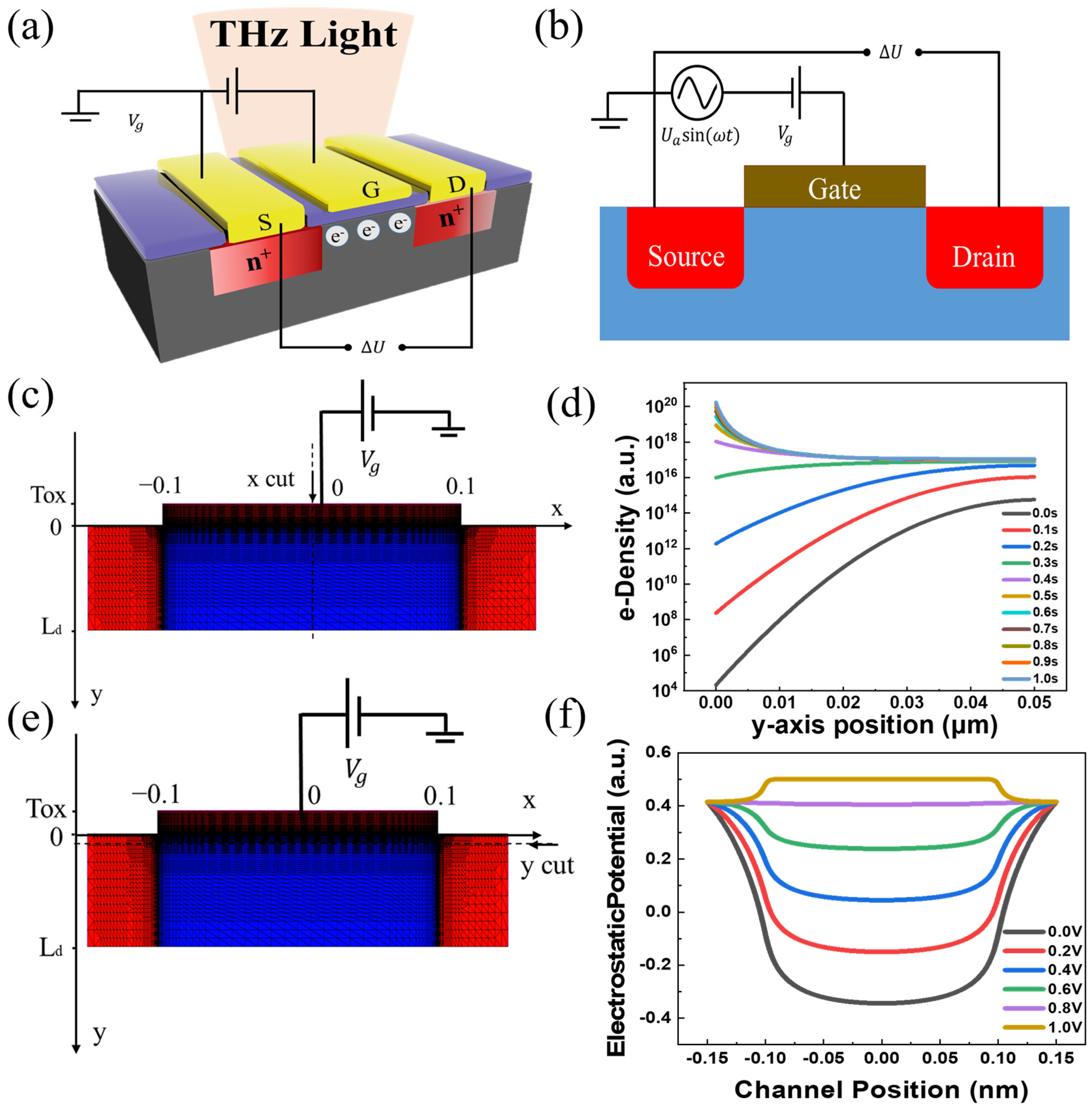
2. Concept of Nonlinear Rectification in a Quasi-One-Dimensional Analysis Model

Harmonic generation is a general characteristic of nonlinear systems; the process of nonlinear rectification in MOSFETs for THz radiation also exhibits this feature [4,5,6,7,8,40]. Following Dyakonov and Shur’s work, the nonlinear properties of plasma waves due to the oscillation of carrier density and velocity play a central role in THz radiation rectification [4,5,6,7,8]. The 2D electron gas will exhibit interesting hydrodynamic behavior [3,4], and the steady current flow in a FET channel can lead to the growth of plasma waves [4]. The AC voltage generated by the incident THz light will act on the channel of the FET, and the nonlinear current–voltage dependence will generate different orders of signal due to the harmonic generation [42,43,44]. Thus, the physical process of THz nonlinear rectification is described as follows.
The surface concentration n in the MOSFET channel is related to the local gate-to-channel voltage swing above the threshold and can be simply determined by the gradual channel approximation [4,5,6,7,8]:
n = C U / q
where C is the gate-to-channel capacitance per unit area; q is the electron charge and U = Ugc(x)UT; Ugc is the gate-to-channel voltage; and UT is the threshold voltage.
The hydrodynamic Euler equation and current continuity equation can be used to understand the dynamic processes of carriers according to the theory of Dyakonov and Shur [4,5,6,7,8], which can be written as follows:
v t + v v x + q m U x + v τ = 0
n t 1 q j n x = 0
where v is the local electron velocity, ∂U/∂x is the longitudinal electric field in the channel, m is the effective electron mass,  τ  is the momentum relaxation time, n is the electron concentration, and jn is the electron current density (for the n-type channel).
Considering Equation (1), the usual continuity equation should be used to calculate Equation (2), which is as follows:
U t + U ν x = 0
These equations coincide with hydrodynamic equations for shallow water. The growth of plasma waves caused by current flow in the FET channel is similar to the shallow water wave [4,5,6,7,8].
Besides, the boundary conditions are as follows:
U 0 , t = V g s + U a sin ω t ,   f o r   x = 0
j L , t = 0 , f o r   x = L
where Vgs is the dc gate-to-source voltage swing, Ua is the amplitude representing the intensity of the THz radiation, and ω is the angular frequency of the incident THz radiation.  U a c = V g s + U a sin ω t  is the external AC voltage induced between the gate and source by the incoming THz wave, and  j = C U ν  is the electron current per unit width.
Then, the solution of Equations (2) and (4) is described in the following form:
ν = ν + ν 1 + ν 2
U = U + U 1 + U 2
where  ν , U  are the time-averaged electron velocity and channel potential, respectively, and  ν n , U n  vary with time with the frequency  n ω , where  ω  is the frequency of the input signal. Since Equations (1) and (2) are nonlinear equations, different harmonics are coupled. It is worth noting that the nonlinear properties of plasma waves can provide the possibility of optical detection [4,5,6,7,8]. However, if the input signal, Ua, is relatively small,  ν 1 , U 1 , are proportional to Ua, while  U U 0 , ν , and  ν 2 , U 2 , are proportional to Ua2, etc. Because the incident THz electromagnetic waves are small in energy, Ua is a small quantity, and Ua2 is an even smaller magnitude. Finally, the embodied higher-order harmonics are dominated by the second-order harmonics.
To the first order in Ua, the following equations are obtained:
v 1 t + u 1 x + v 1 τ = 0
u 1 t + s 2 v 1 x = 0
where u1 = eU1/m and s = (eU0/m)1/2 is the plasma wave velocity. Retaining the second-order time-independent terms, we find the following:
d d x u + ν 1 2 2 + ν τ = 0
d d x ( s 2 v + u 1 ν 1 ) = 0
Here,  u = e U / m  and the angular brackets denote the time averaging over the period  2 π / ω . The boundary conditions for (9)–(12) follow from (5) and (6):
u 1 0 = e m U a c o s ω t
u 0 = e m U 0
v L = v 1 L = 0
For the boundary conditions given by (14) and (15), the integration of (11) and (12) with respect to x yields the following:
Δ u = u L u 0 = 1 2 v 1 2 0 1 τ 0 L v d x
v = u 1 v 1 s 2
Furthermore, the evaluation of  Δ u  from solving the plasma wave dispersion equation, yields the detector response  Δ U = m Δ u / e , which is the constant source-to-drain voltage induced by the incoming ac signal [4,5,6,7,8].
Δ U V g s = 1 4 U a U 0 2 f ω
where
f ω = 1 + 2 ω τ 1 + ω τ 2
Depending on the collision-induced damping of the plasma wave oscillations in the channel, the detection mode is composed of resonant and non-resonant modes, which are determined by the excitation frequency ω and the momentum relaxation time τ.
When  ω τ 1 , the detector works as a resonant detector. The damping of the plasma oscillations is small under the illumination of incident light. The plasma waves reflect between the two boundaries of the channel, causing continuous plasma wave oscillation. The resonance occurs at a specific frequency  ω N = ω 0 ( 2 N + 1 )  leading to a sharp resonance,  ω 0 = π s / 2 L g , s is the plasma wave velocity and Lg is the channel length [4,5,6,7,8,24,25].
On the other hand, the detector works in the nonresonant mode due to the overdamping of the plasma wave when  ω τ 1 . In this case, the DC voltage between the source and drain is a constant. Compared with the case in the non-resonant mode, the generated photoresponse signal could be improved several times in the resonant mode [4,5,6,7,8]. However, several factors, such as channel length and phonons or impurity scattering processes, could limit the signal, which is usually prominent at room temperature. Therefore, we only focus on the THz detector operating in the non-resonant mode at room temperature [4,5,6,7,8].
Theoretically, Equations (1) and (2) indicate the physics of 2D electrons and plasma waves in a simple form. Nonlinear properties of the 2D electron gas lead not only to the rectification of the incoming electromagnetic radiation but also to the emergence of the signal with the second-order and higher harmonics of the incoming radiation [4,5,6,7,8]. It can be seen from Equation (19) that the photoresponse changes only by a factor of three, even when the parameter  ω τ  increases from zero to a very high value. Even though the underlying physical process may be different, the voltage-tunability of FETs endows them with unique advantages to reach higher performance.

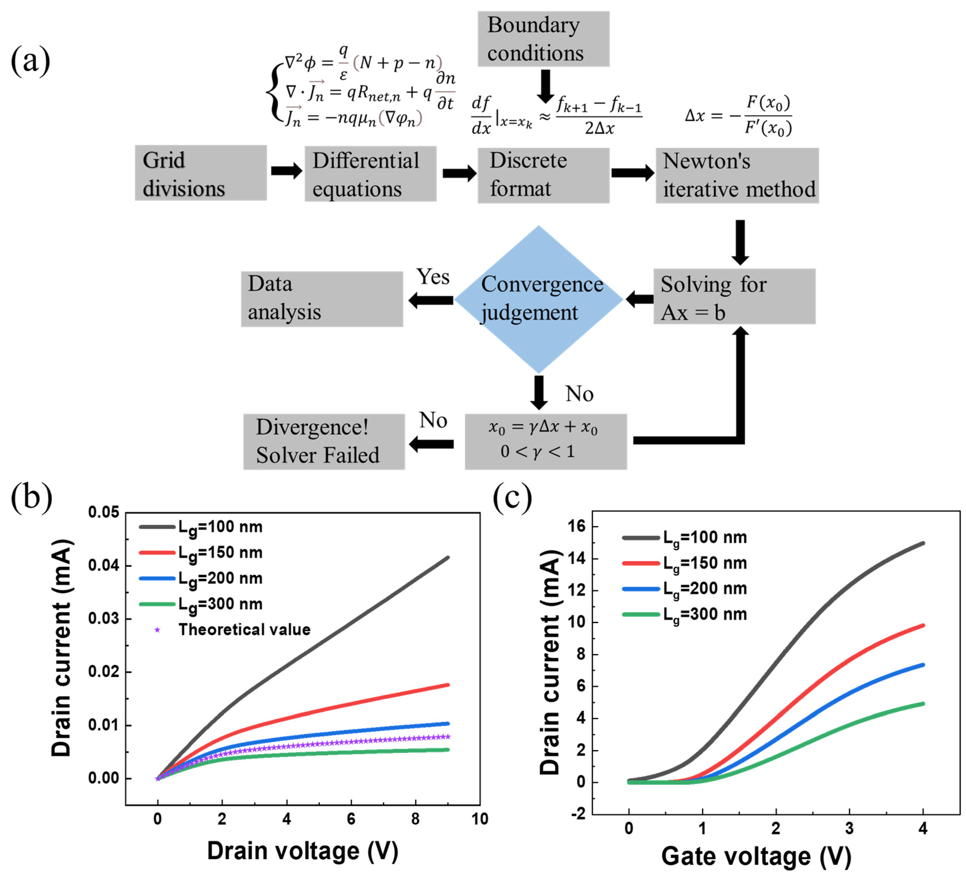
3. Simulation Model and Equations

Based upon the simplest description of nonlinear rectification in one-dimensional terms, we would like to introduce more intricate situations of nonequilibrium dynamics when considering realistic devices. In this work, Sentaurus Technology Computer-Aided Design (TCAD L-2016.03-SP2) simulation is explored via the hydrodynamic/drift-diffusion transport model with extensive incorporation of different physical quantities, open circuit boundary conditions, etc., which describes the plasma wave in the MOSFET channel in a self-consistent manner [4,48,49,50]. The drift-diffusion transport model is used when in thermodynamic equilibrium [50]. When further considering the lattice and electron temperatures, we will use the hydrodynamic model included in the software for the simulation [51,52,53]. During the simulation process, the drift-diffusion model, the Mobility model, the Hydrodynamic model and the RSH (Shockley–Read–Hall) model contained in the simulator are fully used. Here, the basic equations used in the Sentaurus Device are described as follows.
Firstly, the software solves the Poisson equation, which is described as follows:
2 ϕ = q ε N + p n
where,  ϕ  is the electrostatic potential, q is the elementary electronic charge,  ε  is the permittivity, n is the electron density, and p is the hole density.
Secondly, the software solves the continuity equation. In addition, in this device, the charge carriers are electrons, which is described as follows:
· J n = q R n e t , n + q n t
where,  R n e t , n  is the electron net recombination rate,  J n  is electron current density.
Thirdly, the software solves the drift-diffusion transport equation, which is described as follows:
J n = n q μ n φ n
where,  φ n  is the Quasi-fermi potential and  μ n  is the electron mobility. During the simulation, the drift-diffusion transport equations can, eventually, be extended to the hydrodynamic equations.
Fourthly, the thermodynamic transport equation differs from drift-diffusion when the lattice temperature equation is solved. However, it is possible to solve the lattice temperature equation even when using the drift-diffusion model.
J n = n q μ n φ n + p n T
where,  p n  is the absolute thermoelectric power and T is the lattice temperature.
Fifthly, when the electron temperature is also considered in the hydrodynamic model in TCAD, the solution equation is the following:
J n = μ n ( n E c + k T n n n k T n ln γ n + λ n f n t d k n T n 1.5 n k T n ln m n )
in Equation (24), the first term takes into account the contribution due to the spatial variations of electrostatic potential, electron affinity, and the band gap. The remaining terms in Equation (24) take into account the contribution due to the gradient of concentration, the carrier temperature, eventually Te in the channel, gradients, and the spatial variation of the effective masse, mn. for Boltzmann statistics, γ n = λ n = 1 . The thermal diffusion constant  f n t d  defaults to zero, which corresponds to the Stratton model in TCAD [51,52]. Theoretically, the carriers absorb photon energy via an interband or intraband transition under radiation, which leads to the average temperature Te rising above the lattice temperature T. This transport model of Equation (24) takes into account the non-equilibrium state between hot carriers and lattice temperature for different channel sizes, which can be used to study the microphysical behavior of hot electrons [51,52,53].
By self-consistently solving the above physical equations, it allows for the description of the microphysical processes at the interior of the device and ensures the accuracy of the simulation results. It will also provide a convenient way to study the nonlinear rectification process in two-dimensional materials, which opens the door for modification of physical and material parameters [29,30,31,32,33,34,35,36,37,38,39].

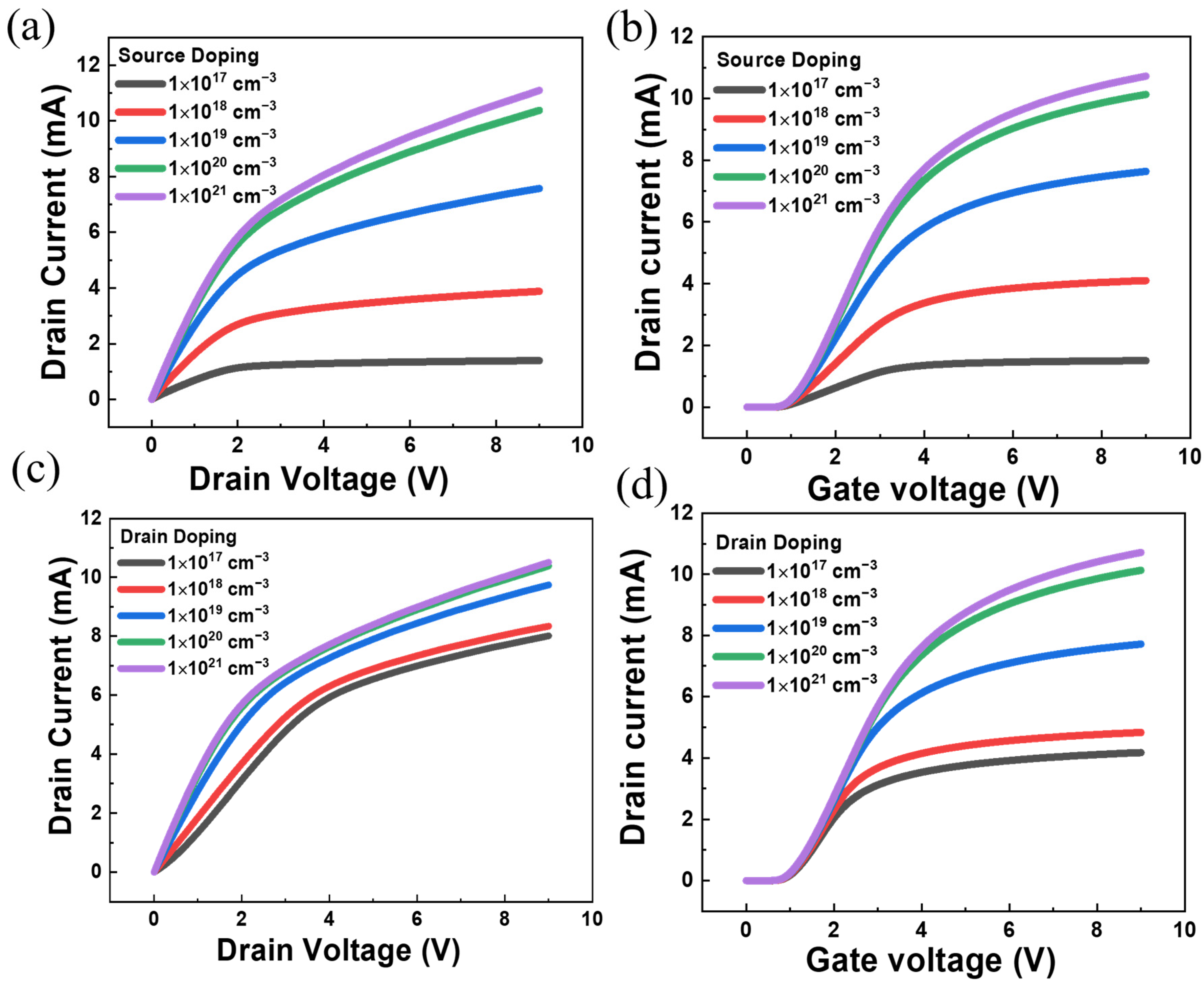
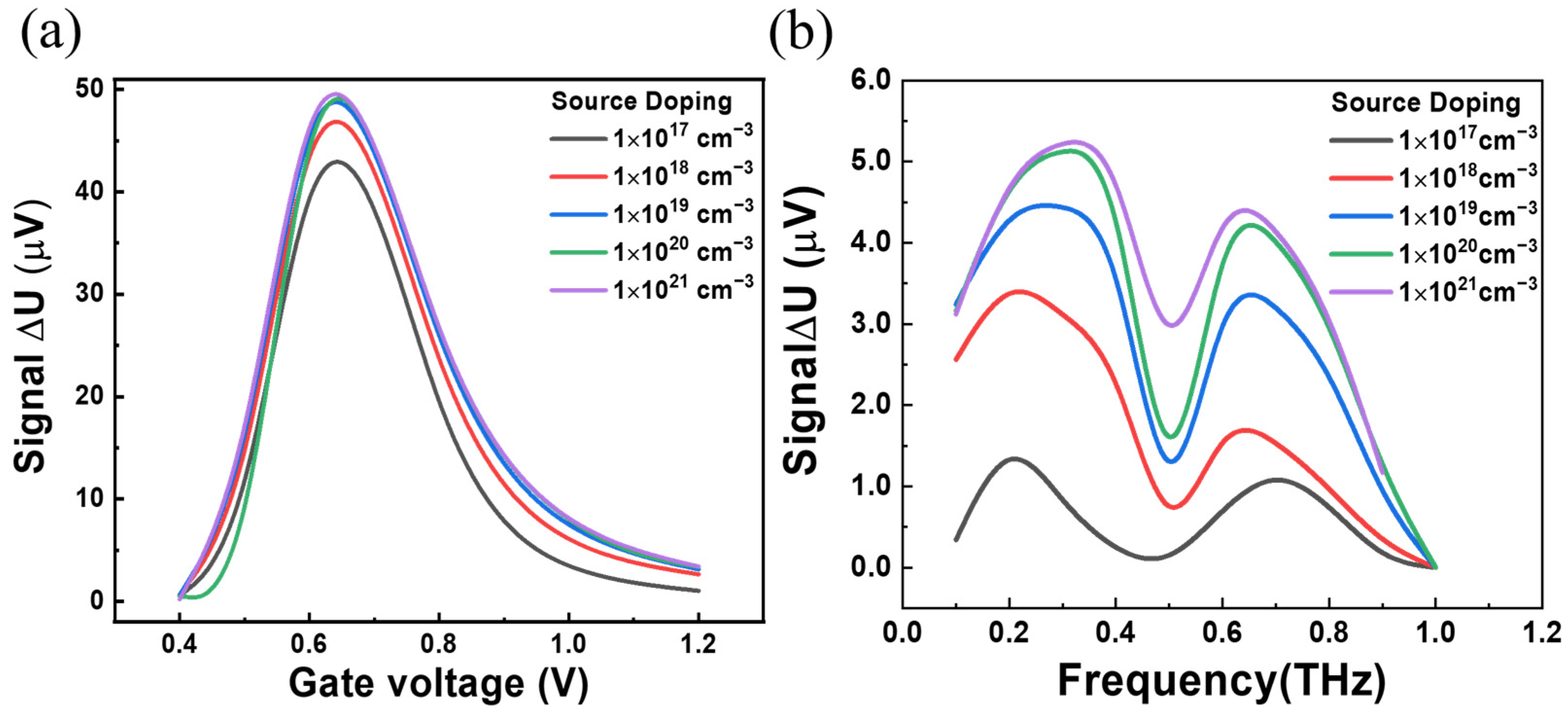
4. Simulation Procedure for Finite Element Analysis

Finite Element Analysis (FEA), by using the numerical calculation method, is an efficient tool to solve all kinds of scientific problems [46,47]. Many problems can be solved by using the finite element method, including electromagnetics, heat transfer, fluid mechanics, stress analysis and other problems [54,55,56]. Meanwhile, it is widely used in scientific fields such as aerospace, automotive, electronics, nuclear science and other fields [50,51]. To date, more and more complex problems in the field of science need to be extracted from their physical models and even consider the interaction of various physical fields. At this moment, FEA can be used to combine a variety of complex physical models and solve complex scientific problems [57,58,59].
The finite element method is used by partitioning a continuous entity into multiple subdomains [54]. In this way, the entity is partitioned into a discrete body with no intersection between each subdomain within the body. The discretized subdomains after partitioning are used as differential elements representing the entity model [60,61]. Separate analysis of each differential element is achieved by solving differential equations created for each element and analyzing the solution results of the differential equations [62,63,64].
The physical field equations that satisfy the behavior of carriers in semiconductors [47] can be solved in TCAD, such as voltage and current magnitude, electron-hole movement and recombination [65,66]. The device is divided into numerous subdomains, and the finite element analysis is performed in each subdomain. Each subdomain of the device is interlinked, such as the contact area between the adjacent subdomains, the type of material added, and the doping concentration of the added material [67,68,69]. The specific simulation steps are described as follows.
The schematic of the silicon-based FETs is shown in Figure 1a. The length of drain Ld and source Ls is 50 nm, the channel length Lg is 100–300 nm, and the  S i O 2  insulating layer is 10 nm. Figure 1b shows the main parameters used in the simulation. The dc gate voltage Vgs and AC voltage Uasin(ωt) are provided between the gate and source (the source terminal is grounded), and Vds is measured with an open circuit boundary condition. Figure 1c shows the finite element division of the mesh structure. Within a specified period of time, the electron concentration of the channel at x = 0 as the gate voltage linearly increases from 0 to 1 V is shown in Figure 1d. During the gate voltage scanning, electron concentration increased by 16 orders of magnitude. Figure 1e,f show the surface electrostatic potential over the range of gate voltage from 0 to 1 V. These figures show that the channel potential continues to rise, and eventually an antipattern layer is formed. Figure 1e shows the cross-section of the channel at y = 3 nm. Figure 1f shows that the surface electrostatic potential rises, extending along the x-axis plane in the channel, as the gate voltage scans. Theoretically, it indicates that the channel is conducting, which can be further used for the internal physical process of the detector. Next, Table 1 lists the important parameters for silicon materials [54].
Figure 2a illustrates the process of finite element simulation and summarizes the main flow of the device simulation. The device is divided into finite grids, and the equations are solved in each grid considering the boundary conditions. The solution results are output after convergence judgment. Figure 2b shows the output current–voltage characteristics of the MOSFET simulated at the gate voltage Vg = 3 V and different gate lengths. Meanwhile, the simulation results have the same trend as the previously calculated theoretical results, which further validates that our finite element simulation is reliable [70]. Figure 2c shows the transfer current–voltage characteristics of the transistor calculated at the drain voltage Vd = 2 V. One can find that the device threshold voltage (Vth) increases as the Lg increases. Specifically, when the Lg is 300 nm, the Vth is 1.23 V, which is significantly larger than that of 100 nm as attributable to a larger parasitic capacitance.
Next, detailed quasi-continuous time-domain simulations are performed to analyze THz mixing in the MOSFET channel. Following Dyakonov and Shur’s work, the nonlinear properties of the 2D electron gas led to THz rectification and the appearance of the signal at the second and higher harmonics under THz radiation [4,5,6,7,8].
Figure 3a shows the time evolution of Vds at the gate bias of 0.7 V with a channel length of 100 nm. It is worth noting that the drain output is comprised of harmonics and self-mixing DC components. To extract the dc response voltage, we performed a Fourier transform to obtain the frequency domain characteristics of the output signal amplitude (Figure 3b). It can be observed that a fundamental tone of ω = 0.2 THz (the incident frequency) is accompanied by a distinguishable DC component (Figure 3b, in the inset). Moreover, as shown in Figure 3c, the second harmonic (0.4 THz) can be observed. Figure 3d–f show the optical response of the device at Vgs = 0.8 V. Figure 3g–i shows the optical response of the device at Vgs = 0.9 V.
In general, the fundamental harmonics (0.2 THz) and the second harmonics (0.4 THz) are in along with the DC component (f~0). As a detector, the DC component can be extracted as the photovoltaic response and is generally used as a signal for THz detection.
By using the hydrodynamic model (corresponding to the drift-diffusion model in software), the open circuit boundary conditions, we simulate the incoming THz wave as a sinusoidal AC signal of frequency (ω), which induces 2D electrons and plasma waves to oscillate in the channel. Here, the oscillations can be captured in a two-dimensional distribution after a rigorous calculation of the transport equation. With the open circuit boundary condition, Figure 4a–c show the simulated results of 2D electron and plasma wave oscillation as a function of time and position along the channel, corresponding to the Lg of 100, 200 and 300 nm.
In agreement with Equations (2), (4) and (18), which describe the plasma wave oscillation with an open circuit boundary condition, we can see a significant asymmetric shift in the electron concentration within one oscillation cycle. The asymmetric shift is caused by the interplay between nonlinear electron oscillation and asymmetric boundary conditions along the channel, leading to a change in potential distribution after time accumulation. Besides, it can be found that the asymmetric offset becomes more pronounced as the Lg increases, which is probably caused by the loading effect reported before [71,72,73,74,75].
Figure 4d shows the drain output direct current (DC) voltage signal ΔU with the change of gate-to-source static voltage for different channel lengths Lg. With the increase in Lg, ΔU initially increases, and then it can be seen that ΔU reaches its peak at Lg = 200 nm. At channels longer than 200 nm, the signal starts to decrease as a result of the loading effect from the access region in the MOSFET device, and the efficiency is reduced at the expense of sub-threshold swing.
Besides, in Figure 4e, we plot the optical response of devices with different Lg from 0.1 to 0.9 THz. It can be observed that the response reaches its lowest value at 0.5 THz. At Lg = 100 nm, the response of the device is smaller than in the other two cases. However, such a process is inefficient at higher frequencies due to the adverse effects of parasitic capacitance and resistance [70]. By taking into account the level of response and reliability, it can be concluded that the optimal length is at Lg = 200 nm.
As a detector, the linear dynamic response is another important parameter that describes the power-dependent properties of targeting weak objects. A good linear relationship between DC output and normalized input radiation power ( U a 2 ) obtained by changing the power by more than an order of magnitude, is shown in Figure 4f [40]. Indeed, it can be inferred from Figure 2, Figure 3 and Figure 4 that the simulated results display very good output and transfer characteristics, and plasma-mixing with high efficiency is given rise at the drain-end under THz irradiation and asymmetric open-circuit boundary conditions. These results validate the reliability and feasibility of our approach for designing and optimizing such types of devices, according to the literature [53].
Following the results of Figure 2c and Figure 4d, an interesting phenomenon can be identified: the Vth is minimal when the Lg is 100 nm, and the saturation curve bends significantly upward as Vd increases. In Figure 4d, the response signal does not grow monotonously after increasing both Vg and Lg and reaches its peak near the threshold gate voltage at Lg = 200 nm. Such a trend cannot be described by simply following Equation (18), from which only a constant voltage drop can be derived, manifesting the discrepancy of gradual channel approximation from the more realistic case that our numerical modeling captures, which means that the physical processes are more complicated when the device is operated below the threshold voltage Vth. Furthermore, our results are also in good agreement with other experimental results for gate voltage-dependent properties, which all show the maximum response near Vth [76,77,78].

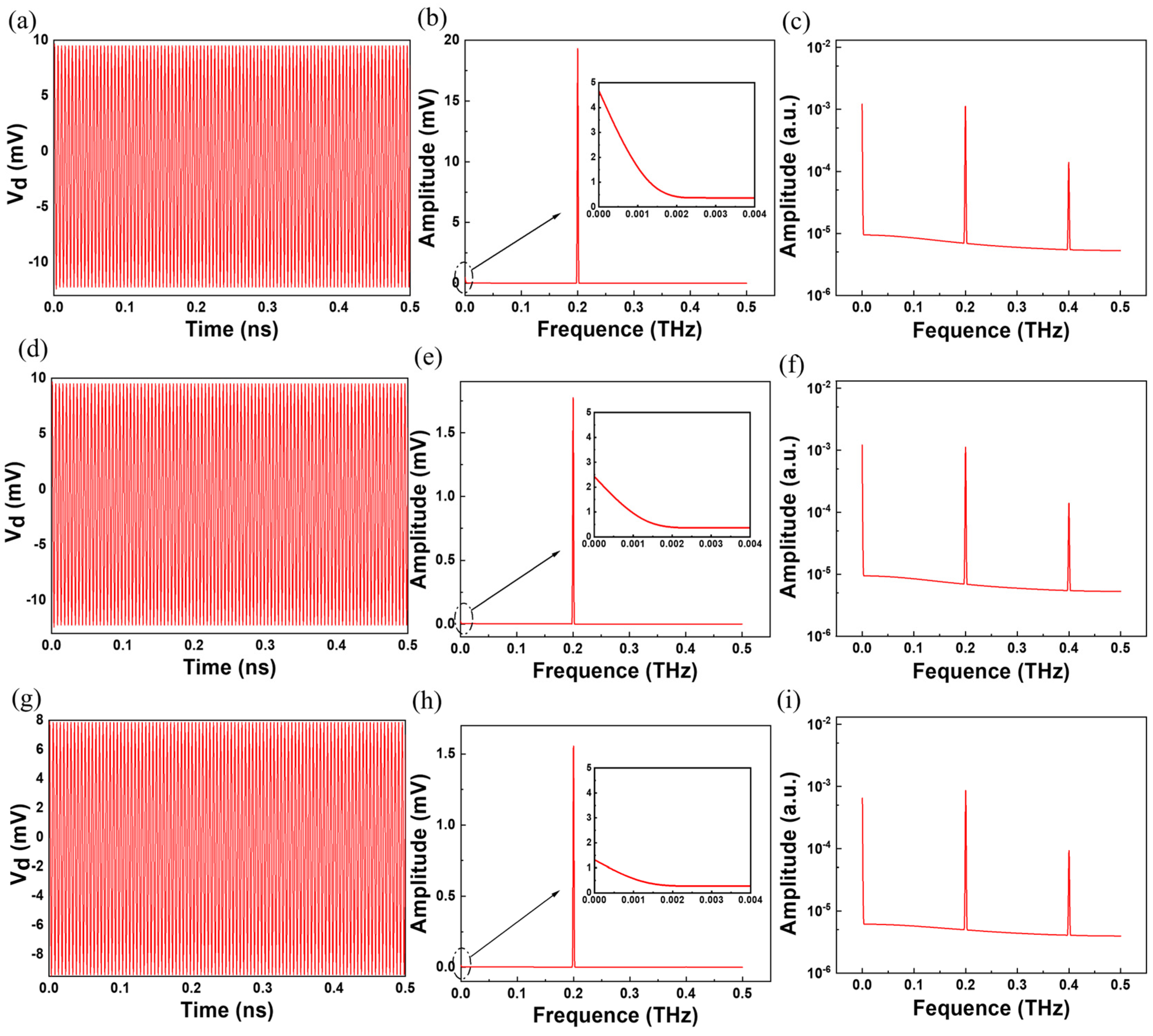
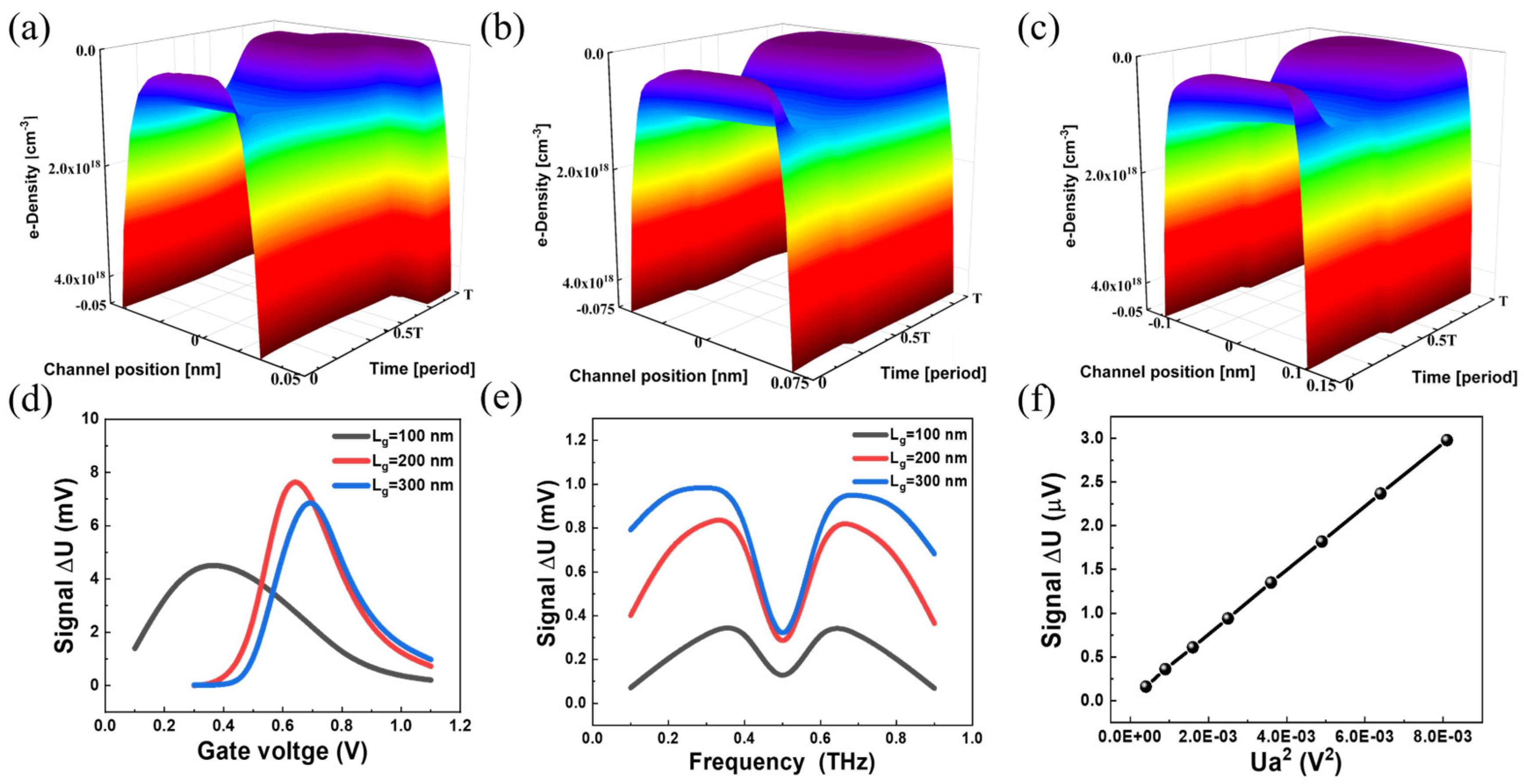
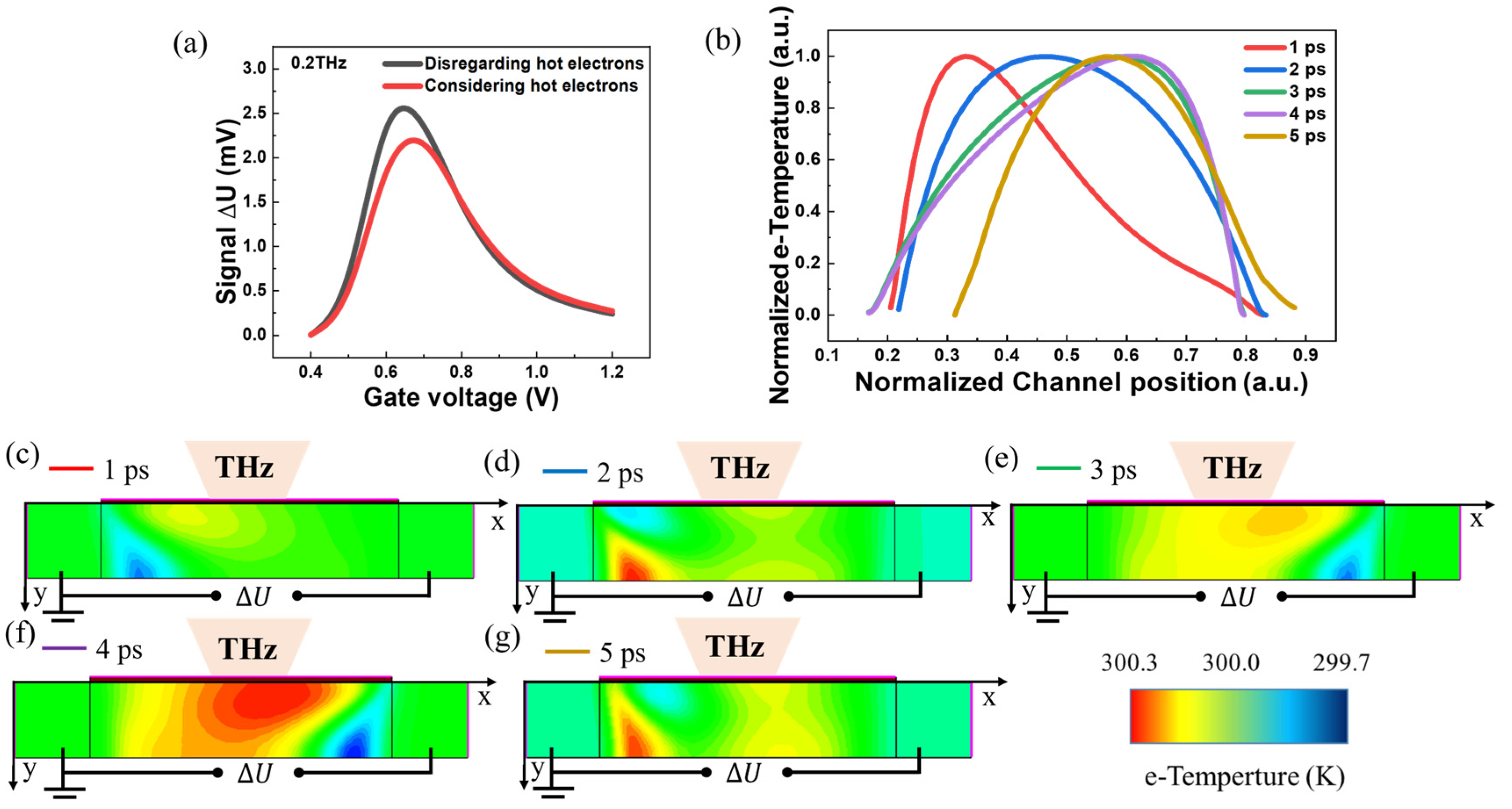
5. Impact of Hot Electrons on Optical Detection

In order to understand the role of non-equilibrium hot electronic processes, we have investigated the physical behavior of carriers in MOSFET short-channel structures. When the channel length of the device is less than the thermal relaxation length of the material, the hot electron effect cannot be neglected in the case of detectors [79].
In 2014, Wang et al. first revealed the physical mechanism of photocurrent generation inside the detector, confirming that THz irradiation can generate a current from hot electrons [80,81]. Under the low energy of terahertz irradiation, it forms hot carriers in the channel with an average temperature Te above the lattice temperature T [82,83]. Theoretically, the formation of hot carriers is much faster than the rate of thermal equilibrium with the lattice, and the hot carrier temperature can remain above the lattice temperature for a considerable period of time [79,82,83]. As a result, it creates a temperature gradient ΔT in the channel. During this period, some of the hot carriers in the channel spontaneously diffused from the high-temperature region to the low-temperature region under the drive of the temperature gradient, which generates current in the channel [79,82,83]. For our simulated process, the hot carriers are hot electrons, whose free diffusion leads to hot electron effects that result in a reduced optical response for THz nonlinear rectification. Theoretically, the ability of hot carrier diffusion is expressed by the Seebeck coefficient, and the potential built into the channel under THz radiation is that  Δ U = S Δ T  [79]. The direction of the resulting current depends on the variation of the material Seebeck system, which is non-monotonic under THz irradiation [80,81,82,83].
The following figure plots the distribution of different electron temperatures during one THz radiation oscillation cycle. In the hydrodynamic model, we have considered the impact of temperature induced by hot electrons on the current. Moreover, other variables are kept constant unless specifically stated.
Figure 5a shows that the optical response is somewhat reduced when considering the physical processes in which hot electrons are present. Therefore, we further analyze the internal variation of the detector during a 0.2 THz oscillation cycle. The electron temperature distribution at different times within a THz oscillation cycle (from 0 to 5 ps) is shown in Figure 5c–g. One can find that the highest temperature point of the electron gradually moves from the source to the drain and finally returns to its original state. We further extract the one-dimensional electron temperature profiles along the horizontal direction of the device (Figure 5b), which intuitively illustrates the movement of the electron temperature peak. In this case, a temperature gradient in the channel is formed due to the non-uniform temperature distribution, which results in the directional diffusion of hot electrons from the drain to the source and a reduction of the non-linear terahertz response at the drain output.
Following the previous device simulations, our finite-element model can be further verified by varying the source/drain doping concentrations and examining the hot electron effect on the output and transfer characteristic curves of the device [84].
Figure 6a–d display the transfer and output characteristic curves by changing the doping at the source and drain, respectively. At first, we calculate the Vth of the transfer curve at different doping concentrations, and Vth is 1.05 V at drain doping of 1017 cm−3, Vth is 1.05 V at drain doping of 1018 cm−3, Vth is 1.07 V at drain doping of 1019 cm−3, Vth is 1.11 V at drain doping of 1020 cm−3, and Vth is 1.12 V at drain doping of 1021 cm−3. The doping concentrations in the range of 1018 to 1020 cm−3 show an obvious effect on the transferring curve, while little effect is observed with doping below or beyond this regime.
Next, we would like to reveal the effect of doping at the source on the device’s performance. The Vth is growing up by increasing the concentration, e.g., Vth is 0.87 V at source doping 1017 cm−3, Vth is 0.97 V at source doping 1018 cm−3, Vth is 1.07 V at source doping 1019 cm−3, Vth is 1.11 V at source doping 1020 cm−3, and Vth is 1.12 V at source doping 1021 cm−3. The output characteristic curves exhibit a saturated trend at intermediate doping concentrations between 1017 and 1020 cm−3. This can reduce the effect of hot electrons on the output characteristics of the device.
Following the above results, the response curves of the device under THz irradiation by changing the doping at the source side are simulated and shown in Figure 7. Under different gate voltage modulations, it can be clearly seen that the device hosts a good response when the doping is between 1019 and 1020 cm−3 in Figure 7a. Furthermore, the highest value of the device response shifts toward a larger Vg as the doping concentration increases. When the doping concentration is below or above the range from 1018 to 1020 cm−3. Based on this, the optimum source doping concentration can be selected.
Furthermore, the optical responses related to different source doping concentrations and different frequencies from 0.1 to 1.0 THz are presented in Figure 7b. It can be found that the optimal doping concentration is between 1019 and 1021 cm−3, and the response remains high with bandwidth exceeding 0.65 THz, which may help in other novel materials for studying THz nonlinear rectification.

6. Conclusions

In this work, we have demonstrated the physical mechanism of nonlinear THz rectification by a finite element method by self-consistently solving the transport equation dynamically. Extensive time-domain simulations are performed to show the carrier dynamics in the channel, considering the hydrodynamic and drift-diffusion models. The competitive behavior between nonlinear rectification and hot electrons induced by the photothermoelectric effect is clearly presented in nanoscale detectors. It is found that the hot-electron effect can be reduced by optimizing the source doping concentrations. Our results provide opportunities for device optimization and understanding the nonlinear THz rectification in other electronic systems, enabling low-energy photon harvesting techniques.

Author Contributions

Y.W. simulated the devices and analyzed the data. Y.W., L.Z., C.Y. and Z.C. discussed the data; L.W., W.L. and X.C. supervised the project; writing—original draft preparation, Y.W.; writing—review and editing L.Z., L.H., L.W. and X.C. All authors commented on the manuscript. All authors have read and agreed to the published version of the manuscript.

Funding

This work was supported by the National Key R&D Program of China (No. 2021YFB2800702), the Zhijiang Lab (No.2021MB0AB01), the Shanghai Natural Science Foundation Project (21ZR1402200, 21ZR1473800), the Shanghai Municipal Science and Technology Major Project (Grant No. 2019SHZDZX01), Analytical Instrumentation Center (#SPST-AIC10112914), Soft Matter Nanofab (#SPST-SMN180827), and Quantum Device Lab, Shanghai Tech University (SQDL).

Institutional Review Board Statement

Not applicable.

Informed Consent Statement

Not applicable.

Data Availability Statement

The datasets used and/or analyzed during the current study are available from the corresponding author on reasonable request.

Conflicts of Interest

The authors declare no conflict of interest.

References

  1. Siegel, P.H. Terahertz technology. IEEE Trans. Microw. Theory Tech. 2002, 50, 910–928. [Google Scholar] [CrossRef]
  2. Akkaş, M.A. Terahertz wireless data communication. Wirel. Netw. 2019, 25, 145–155. [Google Scholar] [CrossRef]
  3. Ueno, Y.; Rungsawang, R.; Tomita, I.; Ajito, K. Terahertz images of biological molecules: Frequency dependence of spatial resolution using a tunable terahertz laser source. Jpn. J. Appl. Phys. 2008, 47, 1315. [Google Scholar] [CrossRef]
  4. Dyakonov, M.; Shur, M. Shallow water analogy for a ballistic field effect transistor: New mechanism of plasma wave generation by dc current. Phys. Rev. Lett. 1993, 71, 2465. [Google Scholar] [CrossRef] [PubMed]
  5. Dyakonov, M.; Shur, M. Two dimensional electronic flute. Appl. Phys. Lett. 1995, 67, 1137–1139. [Google Scholar] [CrossRef]
  6. Dyakonov, M.; Shur, M. Detection, mixing, and frequency multiplication of terahertz radiation by two-dimensional electronic fluid. IEEE Trans. Electron Devices 1996, 43, 380–387. [Google Scholar] [CrossRef]
  7. Dyakonov, M.I.; Shur, M.S. Plasma wave electronics: Novel terahertz devices using two dimensional electron fluid. IEEE Trans. Electron Devices 1996, 43, 1640–1645. [Google Scholar] [CrossRef]
  8. Knap, W.; Dyakonov, M.; Coquillat, D.; Teppe, F.; Dyakonova, N.; Łusakowski, J.; Karpierz, K.; Sakowicz, M.; Valusis, G.; Seliuta, D. Field effect transistors for terahertz detection: Physics and first imaging applications. J. Infrared Millim. Terahertz Waves 2009, 30, 1319–1337. [Google Scholar] [CrossRef] [Green Version]
  9. Fang, T.; Liu, Z.-Y.; Liu, L.-Y.; Li, Y.-Y.; Liu, J.-Q.; Liu, J.; Wu, N.-J. Detection of 3.0 THz wave with a detector in 65 nm standard CMOS process. In Proceedings of the 2017 IEEE Asian Solid-State Circuits Conference (A-SSCC), Seoul, Republic of Korea, 6–8 November 2017; pp. 189–192. [Google Scholar]
  10. Jungemann, C.; Linn, T.; Bittner, K.; Brachtendorf, H.-G. Numerical investigation of plasma effects in silicon MOSFETs for THz-wave detection. Solid-State Electron. 2017, 128, 129–134. [Google Scholar] [CrossRef]
  11. Khan, M.I.W.; Kim, S.; Park, D.-W.; Kim, H.-J.; Han, S.-K.; Lee, S.-G. Nonlinear analysis of nonresonant THz response of MOSFET and implementation of a high-responsivity cross-coupled THz detector. IEEE Trans. Terahertz Sci. Technol. 2017, 8, 108–120. [Google Scholar] [CrossRef]
  12. Liu, Z.; Liu, L.; Zhang, Z.; Liu, J.; Wu, N. Terahertz detector for imaging in 180-nm standard CMOS process. Sci. China Inf. Sci. 2017, 60, 082401. [Google Scholar] [CrossRef]
  13. Daher, C.; Torres, J.; Iñiguez-De-La-Torre, I.; Nouvel, P.; Varani, L.; Sangaré, P.; Ducournau, G.; Gaquière, C.; Mateos, J.; González, T. Room temperature direct and heterodyne detection of 0.28–0.69-THz waves based on GaN 2-DEG unipolar nanochannels. IEEE Trans. Electron Devices 2015, 63, 353–359. [Google Scholar] [CrossRef] [Green Version]
  14. Tanigawa, T.; Onishi, T.; Takigawa, S.; Otsuji, T. Enhanced responsivity in a novel AlGaN/GaN plasmon-resonant terahertz detector using gate-dipole antenna with parasitic elements. In Proceedings of the 68th Device Research Conference, Notre Dame, IN, USA, 21–23 June 2010; pp. 167–168. [Google Scholar]
  15. Antonov, A.; Gavrilenko, V.; Maremyanin, K.; Morozov, S.; Teppe, F.; Knap, W. Resonance detection of terahertz radiation in submicrometer field-effect GaAs/AlGaAs transistors with two-dimensional electron gas. Semiconductors 2009, 43, 528–531. [Google Scholar] [CrossRef]
  16. Javadi, E.; Shahabadi, M.; Masoumi, N.; Notario, J.A.D.; Meziani, Y.M.; Perez, J.E.V. Terahertz detection and imaging using an uncooled off-the-shelf GaN high electron mobility field-effect transistor. In Proceedings of the 2017 Iranian Conference on Electrical Engineering (ICEE), Tehran, Iran, 2–4 May 2017; pp. 409–411. [Google Scholar]
  17. Sangaré, P.; Ducournau, G.; Grimbert, B.; Brandli, V.; Faucher, M.; Gaquière, C.; Íñiguez-de-la-Torre, A.; Íñiguez-de-la-Torre, I.; Millithaler, J.F.; Mateos, J. Experimental demonstration of direct terahertz detection at room-temperature in AlGaN/GaN asymmetric nanochannels. J. Appl. Phys. 2013, 113, 034305. [Google Scholar] [CrossRef] [Green Version]
  18. Suzuki, D.; Oda, S.; Kawano, Y. Gate-voltage tunable terahertz detection by a GaAs/AlGaAs quantum device. In Proceedings of the 2012 37th International Conference on Infrared, Millimeter, and Terahertz Waves, Wollongong, Australia, 23–28 September 2012; pp. 1–2. [Google Scholar]
  19. Suzuki, D.; Oda, S.; Kawano, Y. GaAs/AlGaAs field-effect transistor for tunable terahertz detection and spectroscopy with built-in signal modulation. Appl. Phys. Lett. 2013, 102, 122102. [Google Scholar] [CrossRef]
  20. Vicarelli, L.; Vitiello, M.; Coquillat, D.; Lombardo, A.; Ferrari, A.C.; Knap, W.; Polini, M.; Pellegrini, V.; Tredicucci, A. Graphene field-effect transistors as room-temperature terahertz detectors. Nat. Mater. 2012, 11, 865–871. [Google Scholar] [CrossRef] [Green Version]
  21. Wang, L.; Liu, C.; Chen, X.; Zhou, J.; Hu, W.; Wang, X.; Li, J.; Tang, W.; Yu, A.; Wang, S.W. Toward sensitive room-temperature broadband detection from infrared to terahertz with antenna-integrated black phosphorus photoconductor. Adv. Funct. Mater. 2017, 27, 1604414. [Google Scholar] [CrossRef]
  22. Zak, A.; Andersson, M.A.; Bauer, M.; Matukas, J.; Lisauskas, A.; Roskos, H.G.; Stake, J. Antenna-integrated 0.6 THz FET direct detectors based on CVD graphene. Nano Lett. 2014, 14, 5834–5838. [Google Scholar] [CrossRef] [Green Version]
  23. Li, Y.; Zhang, Y.; Li, T.; Li, M.; Chen, Z.; Li, Q.; Zhao, H.; Sheng, Q.; Shi, W.; Yao, J. Ultrabroadband, ultraviolet to terahertz, and high sensitivity CH3NH3PbI3 perovskite photodetectors. Nano Lett. 2020, 20, 5646–5654. [Google Scholar] [CrossRef]
  24. Li, Y.; Zhang, Y.; Li, T.; Tang, X.; Li, M.; Chen, Z.; Li, Q.; Sheng, Q.; Shi, W.; Yao, J. A fast response, self-powered and room temperature near infrared-terahertz photodetector based on a MAPbI 3/PEDOT: PSS composite. J. Mater. Chem. C 2020, 8, 12148–12154. [Google Scholar] [CrossRef]
  25. Lu, J.-Q.; Shur, M.S.; Hesler, J.L.; Sun, L.; Weikle, R. Terahertz detector utilizing two-dimensional electronic fluid. IEEE Electron Device Lett. 1998, 19, 373–375. [Google Scholar]
  26. Knap, W.; Kachorovskii, V.; Deng, Y.; Rumyantsev, S.; Lü, J.-Q.; Gaska, R.; Shur, M.; Simin, G.; Hu, X.; Khan, M.A. Nonresonant detection of terahertz radiation in field effect transistors. J. Appl. Phys. 2002, 91, 9346–9353. [Google Scholar] [CrossRef]
  27. Lü, J.-Q.; Shur, M.S. Terahertz detection by high-electron-mobility transistor: Enhancement by drain bias. Appl. Phys. Lett. 2001, 78, 2587–2588. [Google Scholar] [CrossRef]
  28. Wang, Y.; Niu, Y.; Chen, M.; Wen, J.; Wu, W.; Jin, Y.; Wu, D.; Zhao, Z. Ultrabroadband, sensitive, and fast photodetection with needle-like EuBiSe3 single crystal. ACS Photonics 2019, 6, 895–903. [Google Scholar] [CrossRef]
  29. Chen, M.; Wang, Y.; Wen, J.; Chen, H.; Ma, W.; Fan, F.; Huang, Y.; Zhao, Z. Annealing temperature-dependent terahertz thermal-electrical conversion characteristics of three-dimensional microporous graphene. ACS Appl. Mater. Interfaces 2019, 11, 6411–6420. [Google Scholar] [CrossRef]
  30. Chen, M.; Wang, Y.; Zhao, Z. Localized Electromagnetic Resonance Enabled THz Photothermoelectric Detection in Graphene. Front. Phys. 2020, 8, 216. [Google Scholar] [CrossRef]
  31. Wen, J.; Niu, Y.; Wang, P.; Chen, M.; Wu, W.; Cao, Y.; Sun, J.-L.; Zhao, M.; Zhuang, D.; Wang, Y. Ultra-broadband self-powered reduced graphene oxide photodetectors with annealing temperature-dependent responsivity. Carbon 2019, 153, 274–284. [Google Scholar] [CrossRef]
  32. Guo, W.; Dong, Z.; Xu, Y.; Liu, C.; Wei, D.; Zhang, L.; Shi, X.; Guo, C.; Xu, H.; Chen, G. Sensitive terahertz detection and imaging driven by the photothermoelectric effect in ultrashort-channel black phosphorus devices. Adv. Sci. 2020, 7, 1902699. [Google Scholar] [CrossRef] [Green Version]
  33. Viti, L.; Hu, J.; Coquillat, D.; Knap, W.; Tredicucci, A.; Politano, A.; Vitiello, M.S. Black phosphorus terahertz photodetectors. Adv. Mater. 2015, 27, 5567–5572. [Google Scholar] [CrossRef] [Green Version]
  34. Viti, L.; Hu, J.; Coquillat, D.; Politano, A.; Consejo, C.; Knap, W.; Vitiello, M.S. Heterostructured hBN-BP-hBN nanodetectors at terahertz frequencies. Adv. Mater. 2016, 28, 7390–7396. [Google Scholar] [CrossRef] [Green Version]
  35. Belopolski, I.; Chang, G.; Cochran, T.A.; Cheng, Z.-J.; Yang, X.P.; Hugelmeyer, C.; Manna, K.; Yin, J.-X.; Cheng, G.; Multer, D. Observation of a linked-loop quantum state in a topological magnet. Nature 2022, 604, 647–652. [Google Scholar] [CrossRef] [PubMed]
  36. Kumar, D.; Hsu, C.-H.; Sharma, R.; Chang, T.-R.; Yu, P.; Wang, J.; Eda, G.; Liang, G.; Yang, H. Room-temperature nonlinear Hall effect and wireless radiofrequency rectification in Weyl semimetal TaIrTe4. Nat. Nanotechnol. 2021, 16, 421–425. [Google Scholar] [CrossRef] [PubMed]
  37. Ma, Q.; Xu, S.-Y.; Shen, H.; MacNeill, D.; Fatemi, V.; Chang, T.-R.; Mier Valdivia, A.M.; Wu, S.; Du, Z.; Hsu, C.-H. Observation of the nonlinear Hall effect under time-reversal-symmetric conditions. Nature 2019, 565, 337–342. [Google Scholar] [CrossRef] [PubMed] [Green Version]
  38. Soluyanov, A.A.; Gresch, D.; Wang, Z.; Wu, Q.; Troyer, M.; Dai, X.; Bernevig, B.A. Type-ii weyl semimetals. Nature 2015, 527, 495–498. [Google Scholar] [CrossRef] [Green Version]
  39. Yan, M.; Huang, H.; Zhang, K.; Wang, E.; Yao, W.; Deng, K.; Wan, G.; Zhang, H.; Arita, M.; Yang, H. Lorentz-violating type-II Dirac fermions in transition metal dichalcogenide PtTe2. Nat. Commun. 2017, 8, 257. [Google Scholar] [CrossRef]
  40. Kovalev, S.; Dantas, R.M.; Germanskiy, S.; Deinert, J.-C.; Green, B.; Ilyakov, I.; Awari, N.; Chen, M.; Bawatna, M.; Ling, J. Non-perturbative terahertz high-harmonic generation in the three-dimensional Dirac semimetal Cd3As2. Nat. Commun. 2020, 11, 2451. [Google Scholar] [CrossRef]
  41. Javadi, E.; But, D.B.; Ikamas, K.; Zdanevičius, J.; Knap, W.; Lisauskas, A. Sensitivity of field-effect transistor-based terahertz detectors. Sensors 2021, 21, 2909. [Google Scholar] [CrossRef]
  42. Ma, Q.; Grushin, A.G.; Burch, K.S. Topology and geometry under the nonlinear electromagnetic spotlight. Nat. Mater. 2021, 20, 1601–1614. [Google Scholar] [CrossRef]
  43. Bahramy, M.; Clark, O.; Yang, B.-J.; Feng, J.; Bawden, L.; Riley, J.; Marković, I.; Mazzola, F.; Sunko, V.; Biswas, D. Ubiquitous formation of bulk Dirac cones and topological surface states from a single orbital manifold in transition-metal dichalcogenides. Nat. Mater. 2018, 17, 21–28. [Google Scholar] [CrossRef] [Green Version]
  44. Fei, Z.; Palomaki, T.; Wu, S.; Zhao, W.; Cai, X.; Sun, B.; Nguyen, P.; Finney, J.; Xu, X.; Cobden, D.H. Edge conduction in monolayer WTe2. Nat. Phys. 2017, 13, 677–682. [Google Scholar] [CrossRef] [Green Version]
  45. Wang, Q.; Zheng, J.; He, Y.; Cao, J.; Liu, X.; Wang, M.; Ma, J.; Lai, J.; Lu, H.; Jia, S. Robust edge photocurrent response on layered type II Weyl semimetal WTe2. Nat. Commun. 2019, 10, 5736. [Google Scholar] [CrossRef] [PubMed] [Green Version]
  46. Barnes, J.J.; Lomax, R.J.; Haddad, G.I. Finite-element simulation of GaAs MESFET’s with lateral doping profiles and submicron gates. IEEE Trans. Electron Devices 1976, 23, 1042–1048. [Google Scholar] [CrossRef]
  47. Buturla, E.; Cottrell, P.; Grossman, B.; Salsburg, K. Finite-element analysis of semiconductor devices: The FIELDAY program. IBM J. Res. Dev. 1981, 25, 218–231. [Google Scholar] [CrossRef]
  48. Frank, D.J.; Dennard, R.H.; Nowak, E.; Solomon, P.M.; Taur, Y.; Wong, H.-S.P. Device scaling limits of Si MOSFETs and their application dependencies. Proc. IEEE 2001, 89, 259–288. [Google Scholar] [CrossRef]
  49. Gaensslen, F. Geometry effects of small MOSFET devices. IBM J. Res. Dev. 1979, 23, 682–688. [Google Scholar] [CrossRef]
  50. Wachutka, G. An Extended Thermodynamic Model for the Simultaneous Simulation of the Thermal and Electrical Behaviour of Semiconductor Devices. In Proceedings of the Sixth International Conference on the Numerical Analysis of Semiconductor Devices and Integrated Circuits (NASECODE VI), Dublin, Ireland, 11–14 July 1989; pp. 409–414. [Google Scholar]
  51. Stratton, R. Diffusion of hot and cold electrons in semiconductor barriers. Phys. Rev. 1962, 126, 2002. [Google Scholar] [CrossRef]
  52. Apanovich, Y.; Blakey, P.; Cottle, R.; Lyumkis, E.; Polsky, B.; Shur, A.; Tcherniaev, A. Numerical simulation of submicrometer devices including coupled nonlocal transport and nonisothermal effects. IEEE Trans. Electron Devices 1995, 42, 890–898. [Google Scholar] [CrossRef]
  53. Palm, E.; Van de Wiele, F. Current lines and accurate contact current evaluation in 2-D numerical simulation of semiconductor devices. IEEE Trans. Electron Devices 1985, 32, 2052–2059. [Google Scholar] [CrossRef]
  54. Nguyen, T.N. Small-Geometry MOS Transistors: Physics and Modeling of Surface-and Buried-Channel MOSFETs; Stanford University: Stanford, CA, USA, 1984. [Google Scholar]
  55. Taur, Y.; Ning, T.H. Fundamentals of Modern VLSI Devices; Cambridge University Press: Cambridge, UK, 1998. [Google Scholar]
  56. Lisauskas, A.; Pfeiffer, U.; Öjefors, E.; Bolìvar, P.H.; Glaab, D.; Roskos, H.G. Rational design of high-responsivity detectors of terahertz radiation based on distributed self-mixing in silicon field-effect transistors. J. Appl. Phys. 2009, 105, 114511. [Google Scholar] [CrossRef]
  57. Hannukainen, A.; Korotov, S.; Křížek, M. The maximum angle condition is not necessary for convergence of the finite element method. Numer. Math. 2012, 120, 79–88. [Google Scholar] [CrossRef]
  58. Hong, J.-W.; Bathe, K.-J. Coupling and enrichment schemes for finite element and finite sphere discretizations. Comput. Struct. 2005, 83, 1386–1395. [Google Scholar] [CrossRef]
  59. Lin, Q.; Liu, J. Counterexamples to the asymptotic expansion of interpolation in finite elements. Adv. Comput. Math. 2007, 27, 167–177. [Google Scholar] [CrossRef]
  60. Odermatt, S.; Ketter, N.; Witzigmann, B. Luminescence and absorption analysis of undoped organic materials. Appl. Phys. Lett. 2007, 90, 221107. [Google Scholar] [CrossRef]
  61. Ruhstaller, B.; Beierlein, T.; Riel, H.; Karg, S.; Scott, J.C.; Riess, W. Simulating electronic and optical processes in multilayer organic light-emitting devices. IEEE J. Sel. Top. Quantum Electron. 2003, 9, 723–731. [Google Scholar] [CrossRef]
  62. Ruhstaller, B.; Carter, S.; Barth, S.; Riel, H.; Riess, W.; Scott, J. Transient and steady-state behavior of space charges in multilayer organic light-emitting diodes. J. Appl. Phys. 2001, 89, 4575–4586. [Google Scholar] [CrossRef]
  63. Tutiš, E.; Bussac, M.; Masenelli, B.; Carrard, M.; Zuppiroli, L. Numerical model for organic light-emitting diodes. J. Appl. Phys. 2001, 89, 430–439. [Google Scholar] [CrossRef]
  64. Walker, A.; Kambili, A.; Martin, S. Electrical transport modelling in organic electroluminescent devices. J. Phys. Condens. Matter 2002, 14, 9825. [Google Scholar] [CrossRef]
  65. Varga, R.S. Matrix Iterative Analysis; Prentice Hall: Englewood Cliffs, NJ, USA, 1962. [Google Scholar]
  66. Bank, R.E.; Rose, D.J.; Fichtner, W. Numerical methods for semiconductor device simulation. SIAM J. Sci. Stat. Comput. 1983, 4, 416–435. [Google Scholar] [CrossRef]
  67. Cheng, S.-W.; Dey, T.K.; Edelsbrunner, H.; Facello, M.A.; Teng, S.-H. Sliver exudation. J. ACM 2000, 47, 883–904. [Google Scholar] [CrossRef]
  68. Edelsbrunner, H. Triangulations and meshes in computational geometry. Acta Numer. 2000, 9, 133–213. [Google Scholar] [CrossRef]
  69. Edelsbrunner, H.; Guoy, D. An experimental study of sliver exudation. Eng. Comput. 2002, 18, 229–240. [Google Scholar] [CrossRef]
  70. Scheinert, S.; Paasch, G.; Schrödner, M.; Roth, H.-K.; Sensfuß, S.; Doll, T. Subthreshold characteristics of field effect transistors based on poly (3-dodecylthiophene) and an organic insulator. J. Appl. Phys. 2002, 92, 330–337. [Google Scholar] [CrossRef]
  71. Gutin, A.; Nahar, S.; Hella, M.; Shur, M. Modeling terahertz plasmonic Si FETs with SPICE. IEEE Trans. Terahertz Sci. Technol. 2013, 3, 545–549. [Google Scholar] [CrossRef]
  72. Ryu, M.W.; Lee, J.S.; Kim, K.S.; Park, K.; Yang, J.-R.; Han, S.-T.; Kim, K.R. High-performance plasmonic THz detector based on asymmetric FET with vertically integrated antenna in CMOS technology. IEEE Trans. Electron Devices 2016, 63, 1742–1748. [Google Scholar] [CrossRef]
  73. El Moutaouakil, A.; Suemitsu, T.; Otsuji, T.; Videlier, H.; Boubanga-Tombet, S.A.; Coquillat, D.; Knap, W. Device loading effect on nonresonant detection of terahertz radiation in dual grating gate plasmon-resonant structure using InGaP/InGaAs/GaAs material systems. Phys. Status Solidi C 2011, 8, 346–348. [Google Scholar] [CrossRef]
  74. Mogab, C. The loading effect in plasma etching. J. Electrochem. Soc. 1977, 124, 1262. [Google Scholar] [CrossRef]
  75. Smirnov, G.M.; Mahan, J.E. Distributed series resistance in photovoltaic devices; intensity and loading effects. Solid-State Electron. 1980, 23, 1055–1058. [Google Scholar] [CrossRef]
  76. Knap, W.; Rumyantsev, S.; Vitiello, M.; Coquillat, D.; Blin, S.; Dyakonova, N.; Shur, M.; Teppe, F.; Tredicucci, A.; Nagatsuma, T. Nanometer size field effect transistors for terahertz detectors. Nanotechnology 2013, 24, 214002. [Google Scholar] [CrossRef]
  77. Stillman, W.; Shur, M.; Veksler, D.; Rumyantsev, S.; Guarin, F. Device loading effects on nonresonant detection of terahertz radiation by silicon MOSFETs. Electron. Lett. 2007, 43, 422–423. [Google Scholar] [CrossRef]
  78. Vitiello, M.S.; Coquillat, D.; Viti, L.; Ercolani, D.; Teppe, F.; Pitanti, A.; Beltram, F.; Sorba, L.; Knap, W.; Tredicucci, A. Room-temperature terahertz detectors based on semiconductor nanowire field-effect transistors. Nano Lett. 2012, 12, 96–101. [Google Scholar] [CrossRef]
  79. Song, J.C.; Rudner, M.S.; Marcus, C.M.; Levitov, L.S. Hot carrier transport and photocurrent response in graphene. Nano Lett. 2011, 11, 4688–4692. [Google Scholar] [CrossRef] [PubMed] [Green Version]
  80. Wang, Y.; Zhang, G.; Qiao, L.; Wei, J.; Zhu, J.-L.; Chen, Z.; Zhao, Z.; Sun, J.-L. Photocurrent response of carbon nanotube-metal heterojunctions in the terahertz range. Opt. Express 2014, 22, 5895–5903. [Google Scholar] [CrossRef] [PubMed]
  81. Wang, Y.; Deng, X.; Zhang, G.; Wei, J.; Zhu, J.-L.; Chen, Z.; Zhao, Z.; Sun, J.-L. Terahertz photodetector based on double-walled carbon nanotube microbundle-metal contacts. Opt. Express 2015, 23, 13348–13357. [Google Scholar] [CrossRef] [PubMed]
  82. Lu, X.; Sun, L.; Jiang, P.; Bao, X. Progress of photodetectors based on the photothermoelectric effect. Adv. Mater. 2019, 31, 1902044. [Google Scholar] [CrossRef]
  83. Nanot, S.; Cummings, A.W.; Pint, C.L.; Ikeuchi, A.; Akiho, T.; Sueoka, K.; Hauge, R.H.; Léonard, F.; Kono, J. Broadband, polarization-sensitive photodetector based on optically-thick films of macroscopically long, dense and aligned carbon nanotubes. Sci. Rep. 2013, 3, 1335. [Google Scholar] [CrossRef] [Green Version]
  84. Preu, S.; Kim, S.; Verma, R.; Burke, P.; Sherwin, M.; Gossard, A. An improved model for non-resonant terahertz detection in field-effect transistors. J. Appl. Phys. 2012, 111, 024502. [Google Scholar] [CrossRef]
Figure 1. (a) MOSFET THz detector structure. (b) Circuit schematic for dynamic simulation. (c,d) Electron concentration of the channel at x = 0 as the gate voltage increases linearly. (e,f) Surface electrostatic potential over the range of gate voltage from 0 to 1 V.
Sensors 23 05367 g001
Figure 2. (a) Flow chart of finite element simulation. (b) Output characteristics of MOSFETs with different channel lengths. (c) Transfer characteristic curves of devices with different channel lengths.
Sensors 23 05367 g002
Figure 3. With Vgs at 0.7 V, (a) Time-domain simulation for Vds. (b) Fourier transform for the response with amplitude at 0.2 THz. (c) FFT was plotted in the logarithmic coordinate system. With Vgs at 0.8 V, (d) Time-domain simulation for Vds. (e) Fourier transform for the response with amplitude at 0.2 THz. (f) FFT was plotted in the logarithmic coordinate system. With Vgs at 0.9 V, (g) Time-domain simulation for Vds. (h) Fourier transform for the response with amplitude at 0.2 THz. (i) FFT was plotted in the logarithmic coordinate system.
Sensors 23 05367 g003
Figure 4. Plot of electron concentration with period and channel position at (a) 100, (b) 200 and (c) 300 nm for asymmetric boundary conditions. (d) Optical response of the device at different gate voltages. (e) Optical response of the device under different THz radiation with frequency changed from 0.1 to 0.9 THz range, different channel length device optical response, and the gate voltage fixed at threshold voltage. (f) Square-law dependence of response on RF signal amplitude at Vgs = 0.7 V.
Sensors 23 05367 g004
Figure 5. (a) Hot-electron effect on the optical response of the device. (b) Distribution of different electron temperatures during a 0.2 THz radiation oscillation cycle. (cg) Two-dimensional distribution of different electron temperatures within one cycle of THz radiation oscillations.
Sensors 23 05367 g005
Figure 6. (a) I-V curves of devices with increasing doping concentrations at the source with a 200 nm channel. (b) Transfer characteristics curves with increasing doping concentrations at the source. (c) I-V curves of devices with increasing doping concentration at drain with a 200 nm channel. (d) Transfer characteristics curves with increasing doping concentrations at the drain with a 200 nm channel.
Sensors 23 05367 g006
Figure 7. (a) Optical response of 200 nm channel devices doped with different source concentrations at different gate voltages. (b) Optical response of 200 nm channel devices doped with different source concentrations at a 0.7 V gate voltage in the frequency range of 0.1 to 0.9 THz.
Sensors 23 05367 g007
Table 1. Physical Properties of Silicon.
PropertiesSi
Effective density of states in the conduction band, Nc (cm−3) 2.8 × 10 19
Effective density of states in the valence band, Nv (cm−3) 1.04 × 10 19
Electron affinity (V)4.05
Energy gap at 300 K (eV)1.12
Minority carrier lifetime (s) 2.5 × 10 3
Electron Mobility (drift) (cm2/V s)1500
Hole Mobility (drift) (cm2/V s)450
Disclaimer/Publisher’s Note: The statements, opinions and data contained in all publications are solely those of the individual author(s) and contributor(s) and not of MDPI and/or the editor(s). MDPI and/or the editor(s) disclaim responsibility for any injury to people or property resulting from any ideas, methods, instructions or products referred to in the content.

