
Front-End Development for Radar Applications: A Focus on 24 GHz Transmitter Design

Abstract
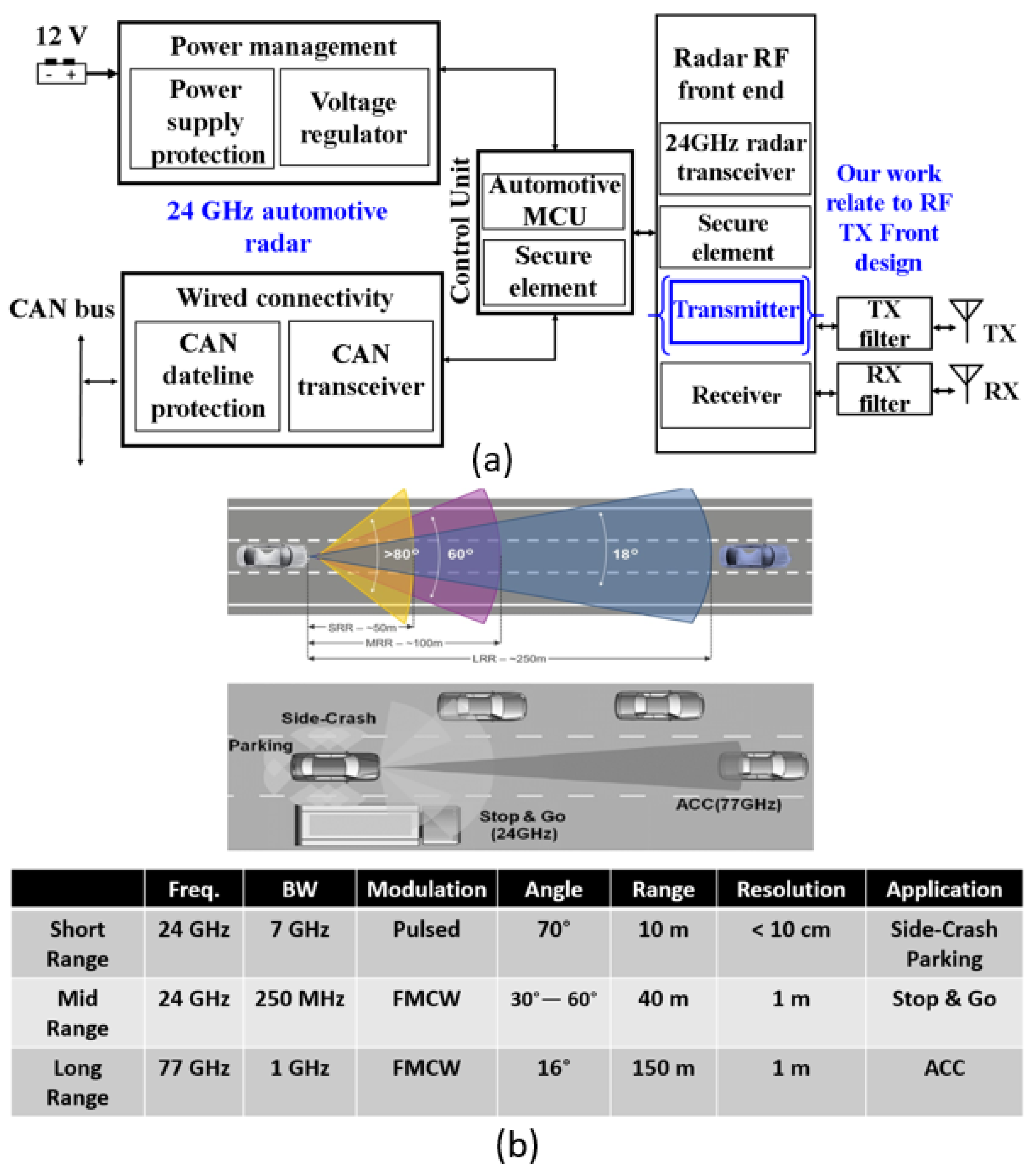
:1. Introduction
1.1. Related Literature
1.2. Main Contributions
2. TX Front-End Integrated Circuit
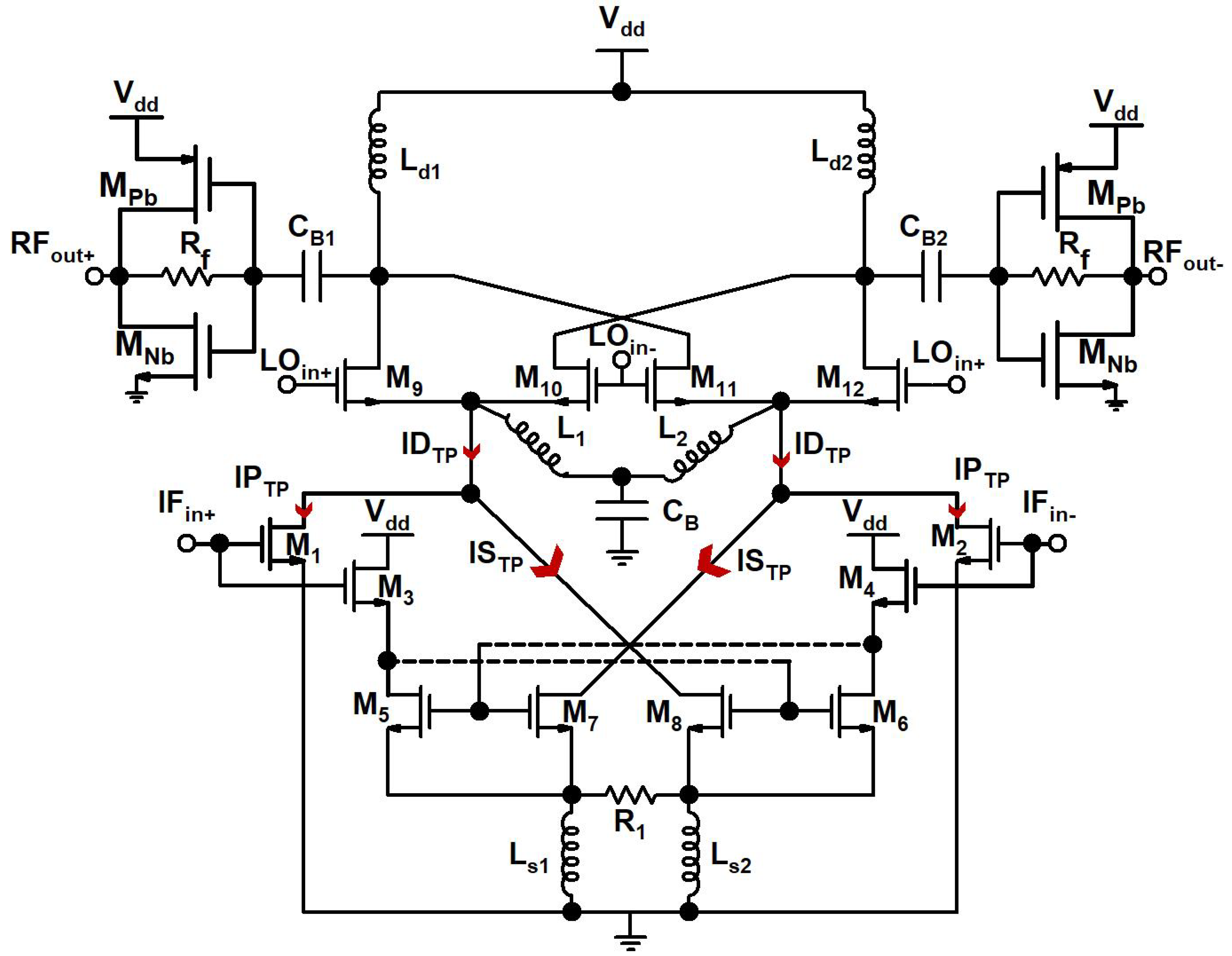
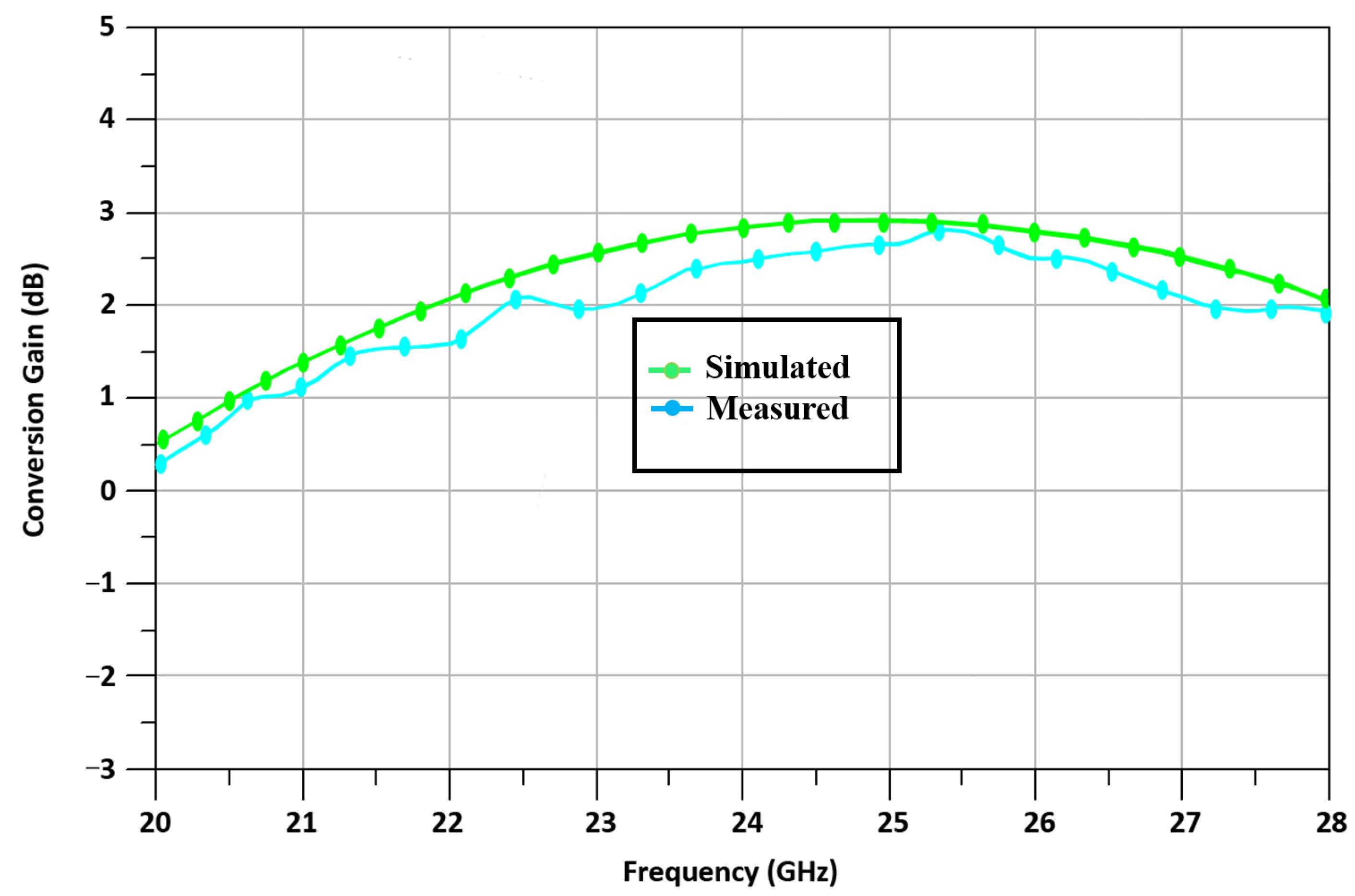
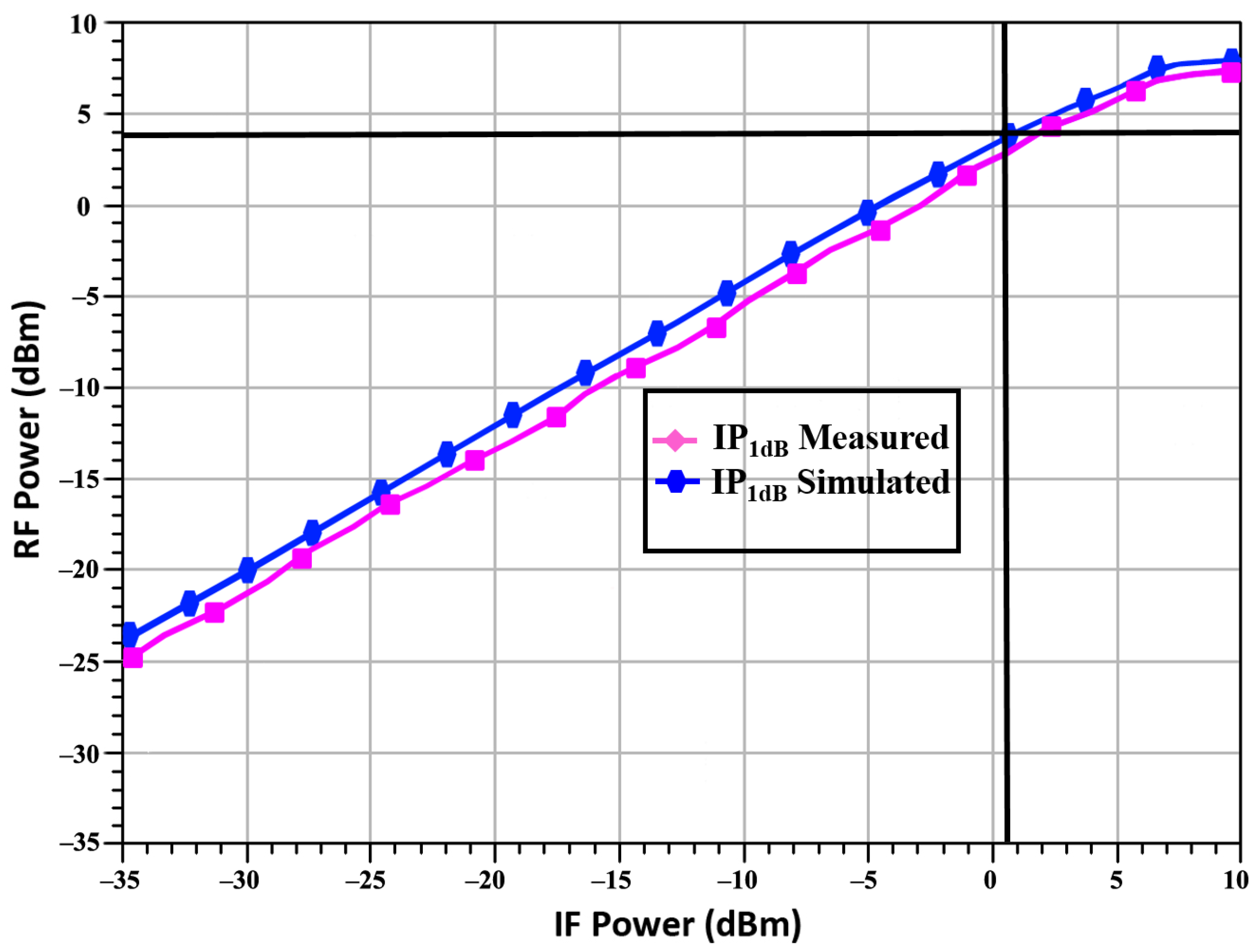
2.1. CMOS Up-Conversion Mixer for TX
2.2. CMOS PA for TX
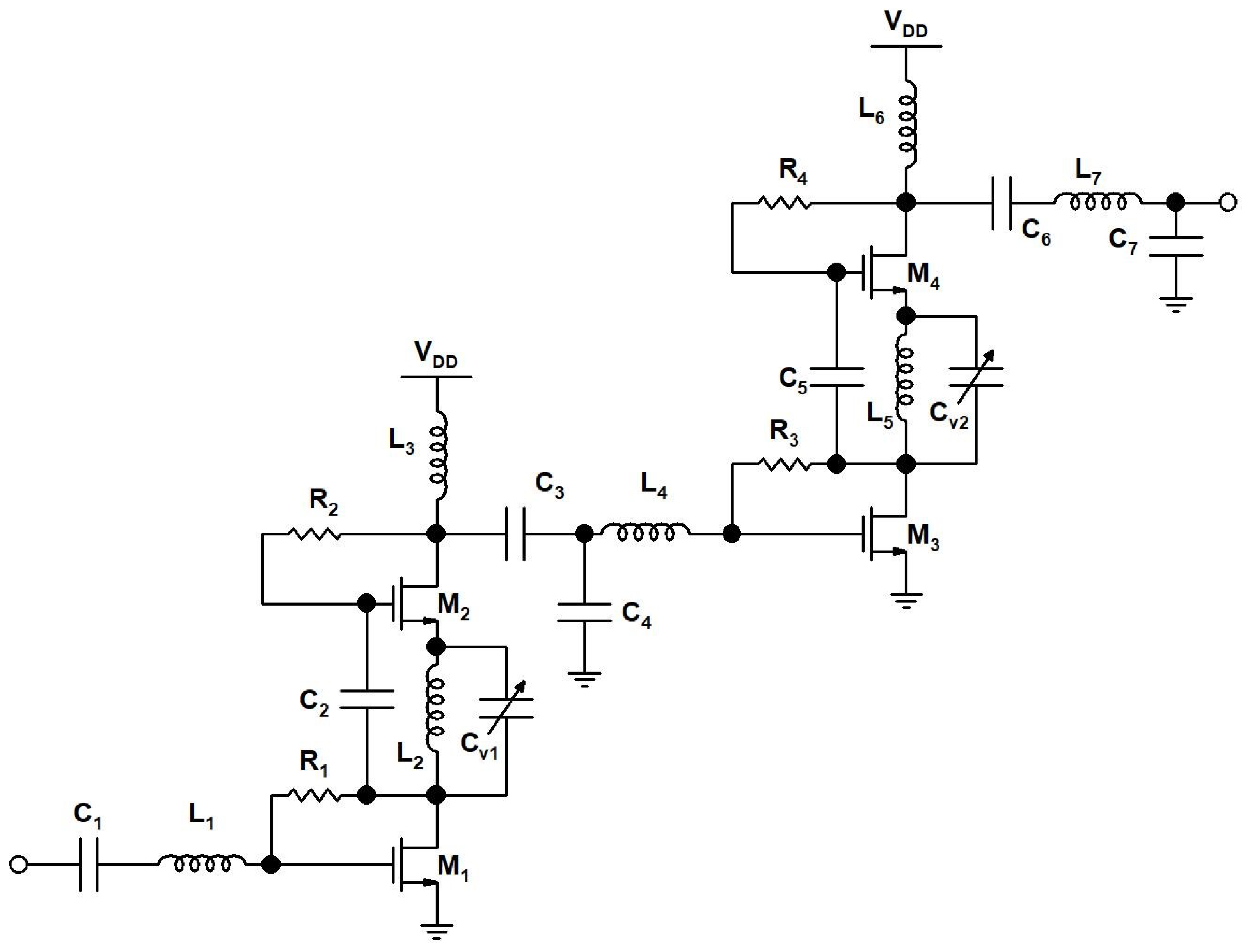
2.3. Proposed TX Front-End: Building Blocks and Integration
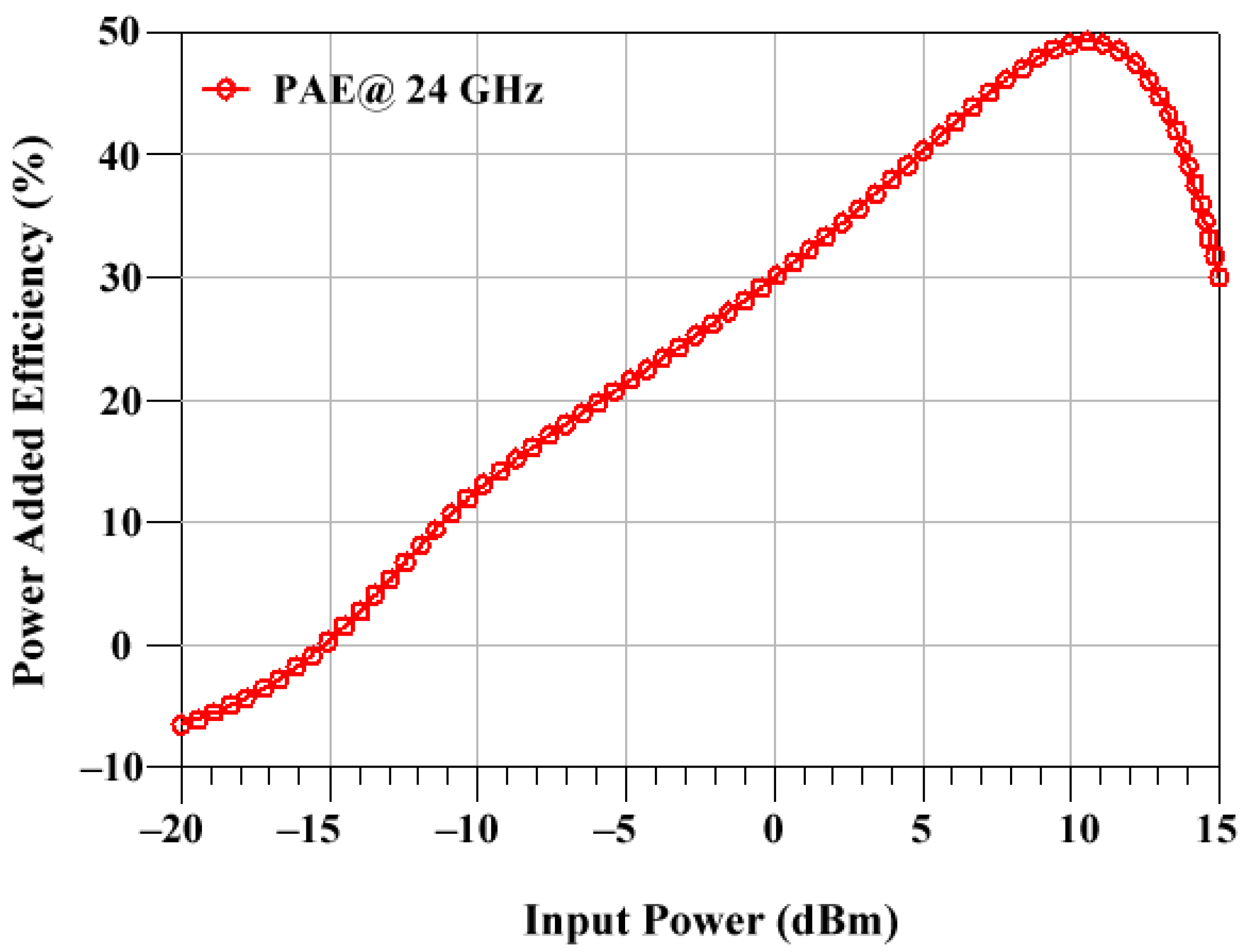
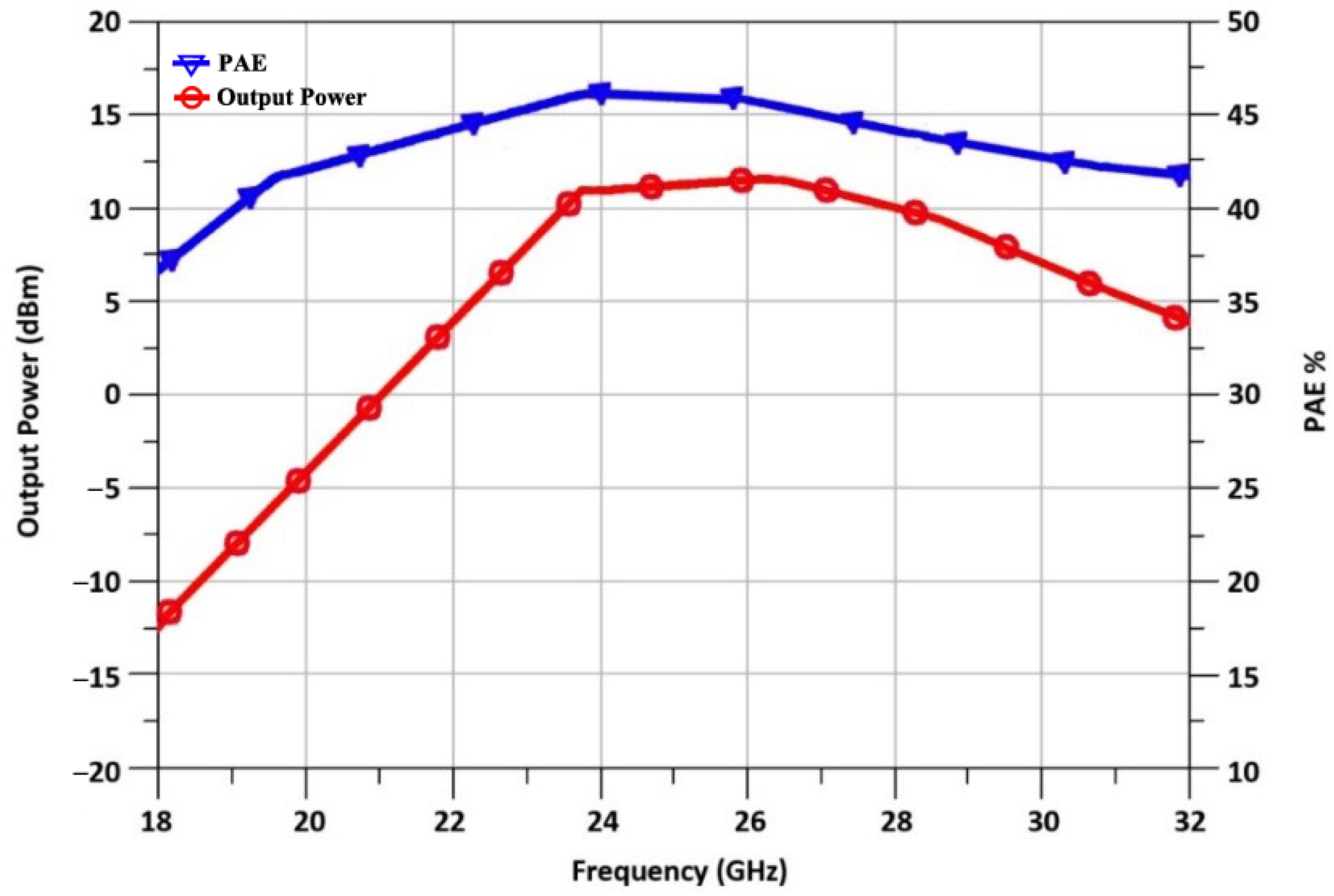
3. Results and Discussion
4. Conclusions and Future Research
Author Contributions
Funding
Institutional Review Board Statement
Informed Consent Statement
Data Availability Statement
Acknowledgments
Conflicts of Interest
References
- Zhang, Y.; He, Y.; Wang, H.; Sun, L.; Su, Y. Ultra-broadband mode size converter using on-chip metamaterial-based Lune-burg lens. ACS Photonics 2021, 8, 202–208. [Google Scholar] [CrossRef]
- Jiang, Y.; Li, X. Broadband cancellation method in an adaptive co-site interference cancellation system. Int. J. Electron. 2022, 109, 854–874. [Google Scholar] [CrossRef]
- Lee, Y.; Kim, S.; Shin, H. A 24 GHz CMOS Direct-Conversion RF Receiver with I/Q Mismatch Calibration for Radar Sensor Applications. Sensors 2022, 22, 8246. [Google Scholar] [CrossRef] [PubMed]
- Wen, C.; Huang, Y.; Davidson, T.N. Efficient Transceiver Design for MIMO Dual-Function Radar-Communication Systems. IEEE Trans. Signal Process. 2023, 71, 1786–1801. [Google Scholar] [CrossRef]
- Zhou, G.; Deng, R.; Zhou, X.; Long, S.; Li, W.; Lin, G.; Li, X. Gaussian inflection point selection for LiDAR hidden echo signal decomposition. IEEE Geosci. Remote Sens. Lett. 2021, 19, 1–5. [Google Scholar] [CrossRef]
- Li, A.; Masouros, C.; Swindlehurst, A.L.; Yu, W. 1-Bit massive MIMO transmission: Embracing interference with symbol-level precoding. IEEE Commun. Mag. 2021, 59, 121–127. [Google Scholar] [CrossRef]
- Tian, H.; Huang, N.; Niu, Z.; Qin, Y.; Pei, J.; Wang, J. Mapping winter crops in China with multi-source satellite imagery and phenology-based algorithm. Remote Sens. 2019, 11, 820. [Google Scholar] [CrossRef]
- Wen, C.; Huang, Y.; Zheng, L.; Liu, W.; Davidson, T.N. Transmit Waveform Design for Dual-Function Radar-Communication Systems via Hybrid Linear-Nonlinear Precoding. IEEE Trans. Signal Process. 2023, 71, 2130–2145. [Google Scholar] [CrossRef]
- Tang, X.; Liu, Z.; Liang, J.; Wu, K.; Bu, Z.; Chen, L. A Fast Fault Diagnosis Method for RF Front-End Modules Based on Adaptive Signal Decomposition and Deep Neural Network. In Proceedings of the IEEE AUTOTESTCON, National Harbor, MD, USA, 28–31 August 2023; pp. 1–5. [Google Scholar]
- Zmrzlak, L.; Blatnik, A.; Scaffardi, M.; Bogoni, A.; Batagelj, B. Transmitter and Receiver Amplifier Chains in X-and Ku-bands of Radio Frequency Front-End for Frequency-Agile Microwave Photonic Radars. In Proceedings of the 2023 30th International Conference on Systems, Signals and Image Processing (IWSSIP), Ohrid, North Macedonia, 27–29 June 2023; pp. 1–5. [Google Scholar]
- Maier, M.; Wäsner, S.; Issakov, V. System Considerations and FMCW Radar Transceiver for Breast Cancer Detection. In Proceedings of the 2023 IEEE MTT-S International Microwave Biomedical Conference (IMBioC), Leuven, Belgium, 11–13 September 2023; pp. 1–3. [Google Scholar]
- Asbeck, P.M.; Rostomyan, N.; Özen, M.; Rabet, B.; Jayamon, J.A. Power amplifiers for mm-wave 5G applications: Tech-nology comparisons and CMOS-SOI demonstration circuits. IEEE Trans. Microw. Theory Tech. 2019, 67, 3099–3109. [Google Scholar] [CrossRef]
- Aoki, I.; Kee, S.D.; Rutledge, D.B.; Hajimiri, A. Fully integrated CMOS power amplifier design using the distributed ac-tive-transformer architecture. IEEE Solid-State Circuits 2002, 37, 371–383. [Google Scholar] [CrossRef]
- Delwar, T.S.; Siddique, A.; Biswal, M.R.; Behera, P.; Choi, Y.; Ryu, J.Y. A 65 nm Duplex Transconductance Path Up-Conversion Mixer for 24 GHz Automotive Short-Range Radar Sensor Applications. Sensors 2022, 22, 594. [Google Scholar] [CrossRef] [PubMed]
- Nguyen, T.K.; Oh, N.J.; Han, S.K.; Lee, S.G. A low-power CMOS RF transmitter front-end for 2.4 GHz ZigBee applications. In Proceedings of the 2006 IEEE Radio and Wireless Symposium, San Diego, CA, USA, 17–19 October 2006; pp. 43–46. [Google Scholar]
- Kwon, D.H.; Li, H.; Chang, Y.; Tseng, R.; Chiu, Y. Digitally equalized CMOS transmitter front-end with integrated power amplifier. IEEE Solid-State Circuits 2010, 45, 1602–1614. [Google Scholar] [CrossRef]
- Nuyts, P.A.; Singerl, P.; Dielacher, F.; Reynaert, P.; Dehaene, W. A fully digital delay line-based GHz range multimode transmitter front-end in 65 nm CMOS. IEEE Solid-State Circuits 2012, 47, 1681–1692. [Google Scholar] [CrossRef]
- Saleem, A.R.; Stadius, K.; Hannula, J.M.; Lehtovuori, A.; Kosunen, M.; Viikari, V.; Ryynänen, J. A 1.5–5 GHz integrated RF transmitter front end for active matching of an antenna cluster. IEEE Trans. Microw. Theory Tech. 2020, 68, 4728–4739. [Google Scholar] [CrossRef]
- Kim, H.; Yoon, I.J.; Yoon, Y.J. A novel fully integrated transmitter front-end with high power-added efficiency. IEEE Trans. Microw. Theory Tech. 2005, 53, 3206–3214. [Google Scholar]
- Sandström, D.; Varonen, M.; Kärkkäinen, M.; Halonen, K.A. A W-band 65 nm CMOS transmitter front-end with 8 GHz IF bandwidth and 20 dB IR ratio. In Proceedings of the 2010 IEEE International Solid-State Circuits Conference-(ISSCC), San Francisco, CA, USA, 7–11 February 2010; pp. 418–419. [Google Scholar]
- Liu, B.; Yi, X.; Yang, K.; Liang, Z.; Feng, G.; Choi, P.; Boon, C.C.; Li, C. A carrier aggregation transmitter front end for 5 GHz WLAN 802.11 ax application in 40 nm CMOS. IEEE Trans. Microw. Theory Tech. 2019, 68, 264–276. [Google Scholar] [CrossRef]
- Shin, B.; Kim, C.; Bae, S.; Moon, H.; Nam, I. A 24 GHz CMOS transmitter front-end for vital signal monitoring radar system. In Proceedings of the 2017 Progress in Electromagnetics Research Symposium-Fall (PIERS-FALL), Singapore, 19–22 November 2017; pp. 1354–1357. [Google Scholar]
- Zhu, W.; Wang, J.; Lv, W.; Zhang, X.; Liao, B.; Zhu, Y.; Wang, Y. A 24–28 GHz power and area efficient 4-element phased-array transceiver front-end with 21.1%/16.6% transmitter peak/OP1dB PAE supporting 2.4 Gb/s in 256-QAM for 5G communications. In Proceedings of the 2020 IEEE Radio Frequency Integrated Circuits Symposium (RFIC), Los Angeles, CA, USA, 4–6 August 2020; pp. 351–354. [Google Scholar]
- Chen, H.S.; Lu, L.H. A 34.8%-PAE CMOS transmitter frontend for 24 GHz FMCW radar applications. In Proceedings of the 2012 IEEE Asian Solid State Circuits Conference (A-SSCC), Kobe, Japan, 12–14 November 2012; pp. 265–268. [Google Scholar]
- Kim, C.Y.; Kim, J.G.; Baek, D.; Hong, S. A circularly polarized balanced radar front-end with a single antenna for 24 GHz radar applications. IEEE Trans. Microw. Theory Tech. 2008, 57, 293–297. [Google Scholar]
- Boroujeni, S.R.; Mazaheri, M.H.; Ituah, S.; Wyrzykowska, A.; Ziabakhsh, S.; Palizban, A.; Chen, G.; El-Gouhary, A.; Ferei-dani, K.; Nezhad-Ahmadi, M.R.; et al. A high-efficiency 27–30 GHz 130 nm Bi-CMOS transmitter front end for SATCOM phased arrays. IEEE Trans. Microw. Theory Tech. 2021, 69, 4977–4985. [Google Scholar] [CrossRef]
- Lee, H.S.; Park, M.; Min, B.W. A 26 GHz transmitter front-end using double quadrature architecture. PLoS ONE 2019, 14, e0216474. [Google Scholar] [CrossRef]
- Saito, N.; Tsukizawa, T.; Shirakata, N.; Morita, T.; Tanaka, K.; Sato, J.; Morishita, Y.; Kanemaru, M.; Kitamura, R.; Shima, T.; et al. A fully integrated 60 GHz CMOS transceiver chipset based on WiGig/IEEE 802.11 ad with built-in self cali-bration for mobile usage. IEEE J. Solid-State Circuits 2013, 48, 3146–3159. [Google Scholar] [CrossRef]
- Okada, K.; Minami, R.; Tsukui, Y.; Kawai, S.; Seo, Y.; Sato, S.; Kondo, S.; Ueno, T.; Takeuchi, Y.; Yamaguchi, T.; et al. 20.3 A 64-QAM 60 GHz CMOS transceiver with 4-channel bonding. In Proceedings of the 2014 IEEE International Solid-State Circuits Conference Digest of Technical Papers (ISSCC), San Francisco, CA, USA, 9–13 February 2014; pp. 346–347. [Google Scholar]
- Zhao, D.; Kulkarni, S.; Reynaert, P. A 60 GHz outphasing transmitter in 40 nm CMOS. IEEE J. Solid-State Circuits 2012, 47, 3172–3183. [Google Scholar] [CrossRef]


| Parameter | Dimension |
|---|---|
| M1∼ M2 | 36 m/65 nm |
| M3 ∼M4 | 64 m/65 nm |
| M5∼ M6 | 36 m/65 nm |
| M7 ∼ M8 | 216 m/65 nm |
| M9 ∼ M12 | 40 m/65 nm |
| MPb ∼ MNb | 90 m/65 nm |
| L1 ∼ L2 | 180 pH |
| Ld1 ∼ Ld2 | 250 pH |
| Ls1 ∼ Ls2 | 150 pH |
| R1 | 2 K |
| Rf | 4 K |
| CB | 80 pF |
| CB1 ∼ CB2 | 145 pF |
| Parameter | Dimension |
|---|---|
| L1 | 0.65 nH |
| L2 | 0.78 nH |
| L3 | 1.7 nH |
| L4 | 0.91 nH |
| L5 | 1.1 nH |
| L6 | 1.8 nH |
| L7 | 1.5 nH |
| R1∼R2 | 73 |
| R3∼R4 | 78 |
| C1∼C3∼C7 | 0.5 pF |
| C2 | 0.87 pF |
| C4 | 0.51 pF |
| C5 | 0.37 pF |
| C6 | 0.41 pF |
| Cv1 | 0.45 pF |
| Cv2 | 0.2 pF |
| Parameter | Supply voltage Technology RF frequency IF frequency | 1.2 V 65 nm CMOS 24 GHz 2.4 GHz |
| Up-Conversion Mixer | Conversion gain Noise figure OP1dB Power consumption Chip area | 2.49 dB 3.9 dB 3.9 dBm 3.24 mW 0.42 mm2 |
| Power Amplifier | Conversion gain IIP3 PAE Psat Chip area | 28.4 ± 0.5 dB 14.5 dBm 47.5% 14.21 dBm 0.406 mm2 |
| TX RF Front-End | Conversion gain S11/S22 OP1dB PAE Psat Chip area | 28.1 dB −13.2/−18.7 dB 10.5 dBm 47% 11.7 3.2 mm2 |
Disclaimer/Publisher’s Note: The statements, opinions and data contained in all publications are solely those of the individual author(s) and contributor(s) and not of MDPI and/or the editor(s). MDPI and/or the editor(s) disclaim responsibility for any injury to people or property resulting from any ideas, methods, instructions or products referred to in the content. |
© 2023 by the authors. Licensee MDPI, Basel, Switzerland. This article is an open access article distributed under the terms and conditions of the Creative Commons Attribution (CC BY) license (https://creativecommons.org/licenses/by/4.0/).
Share and Cite
Delwar, T.S.; Aras, U.; Siddique, A.; Lee, Y.; Ryu, J.-Y. Front-End Development for Radar Applications: A Focus on 24 GHz Transmitter Design. Sensors 2023, 23, 9704. https://doi.org/10.3390/s23249704
Delwar TS, Aras U, Siddique A, Lee Y, Ryu J-Y. Front-End Development for Radar Applications: A Focus on 24 GHz Transmitter Design. Sensors. 2023; 23(24):9704. https://doi.org/10.3390/s23249704
Chicago/Turabian StyleDelwar, Tahesin Samira, Unal Aras, Abrar Siddique, Yangwon Lee, and Jee-Youl Ryu. 2023. "Front-End Development for Radar Applications: A Focus on 24 GHz Transmitter Design" Sensors 23, no. 24: 9704. https://doi.org/10.3390/s23249704