
T-ray Wavelength Decoupled Imaging and Profile Mapping of a Whole Wafer for Die Sorting and Analysis


Abstract
:1. Introduction
2. Materials and Methods
2.1. Mechanics of Cameraless Image Formation: Decoupling the Wavelength
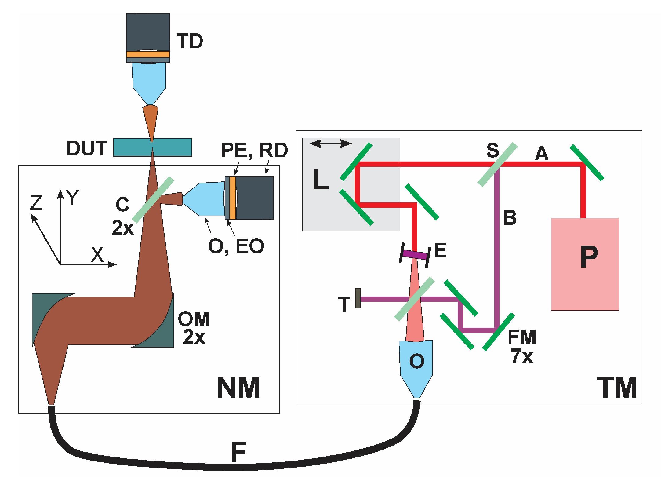
2.2. Experimental
3. Results
3.1. Comparison of the T-ray Image of Die Features with Optical Images
3.2. Profile along a Row of Dies
3.3. A Criterion for Sorting Good Dies
4. Discussion
5. Conclusions
Funding
Institutional Review Board Statement
Informed Consent Statement
Data Availability Statement
Conflicts of Interest
References
- Maynard, D.N.; Rosner, R.J.; Kerbaugh, M.L.; Hamilton, R.A.; Bentlage, J.R.; Boye, C.A. Wafer Line Productivity Optimization in a Multi-Technology Multi-Part-Number Fabricator. In Proceedings of the IEEE/SEMI 1998 IEEE/SEMI Advanced Semiconductor Manufacturing Conference and Workshop (Cat. No.98CH36168), Boston, MA, USA, 23–25 September 1998; pp. 34–42. [Google Scholar] [CrossRef]
- Chao, L.-C.; Tong, L.-I. Wafer defect pattern recognition by multi-class support vector machines by using a novel defect cluster index. Expert Syst. Appl. 2009, 36, 10158–10167. [Google Scholar] [CrossRef]
- Murphy, B.T. Cost-Size Optima of Monolithic Integrated Circuits. Proc. IEEE 1964, 52, 1537–1545. [Google Scholar] [CrossRef]
- Stapper, C.H. Defect Density Distribution for LSI Yield Calculations. IEEE Trans. Electron Devices 1973, 20, 655–657. [Google Scholar] [CrossRef]
- Rahman, A.; Rahman, A.K. Nanoscale Metrology of Line Patterns on Semiconductor by Continuous Wave Terahertz Multispectral Reconstructive 3-D Imaging Overcoming the Abbe Diffraction Limit. IEEE Trans. Semicond. Manuf. 2019, 32, 7–13. [Google Scholar] [CrossRef]
- Abbe, E. Beiträge zur Theorie des Mikroskops und der mikroskopischen Wahrnehmung. Arch. Mikrosk. Anat. 1873, 9, 413. [Google Scholar] [CrossRef]
- Rahman, A. Terahertz Multispectral Imaging of Epitaxially Grown Semiconductors’ Lattice Defects. In Proceedings of the 2017 28th Annual SEMI Advanced Semiconductor Manufacturing Conference (ASMC) 2017, Saratoga Springs, NY, USA, 15–18 May 2017; pp. 45–50. [Google Scholar] [CrossRef]
- Rahman, A.; Tanzella, F.; Rahman, A.K.; Page, C.; Godes, R. Lattice Dilation of Plasma Sprayed Nickel Film Quantified by High Resolution Terahertz Imaging. Nov. Res. Sci. 2019, 2. [Google Scholar] [CrossRef]
- Campregher, N.; Cheung, P.Y.K.; Constantinides, G.A.; Vasilko, M. Analysis of yield loss due to random photolithographic defects in the interconnect structure of FPGAs. In Proceedings of the 2005 ACM/SIGDA 13th International Symposium on Field-Programmable Gate Arrays—FPGA ’05, Monterey, CA, USA, 20–22 February 2005. [Google Scholar] [CrossRef]
- Available online: https://semiconductor.samsung.com/support/tools-resources/fabrication-process/eight-essential-semiconductor-fabrication-processes-part-8-eds-electrical-die-sorting-for-the-perfect-chips/ (accessed on 5 March 2023).
- Available online: https://www.kla.com/products/packaging-manufacturing/die-sorting-and-inspection (accessed on 5 March 2023).


| # | M | D | % | Comment |
|---|---|---|---|---|
| Die 1 | 35,042,996 | - | - | Ref |
| Die 2 | 31,875,631 | 3,167,365 | 9 | Fail |
| Die 3 | 33,863,572 | 1,179,424 | 3 | Pass |
| Die 4 | 35,586,599 | −543,603 | −2 | Pass |
| Die 5 | 36,832,244 | −1,789,248 | −5 | Pass |
Disclaimer/Publisher’s Note: The statements, opinions and data contained in all publications are solely those of the individual author(s) and contributor(s) and not of MDPI and/or the editor(s). MDPI and/or the editor(s) disclaim responsibility for any injury to people or property resulting from any ideas, methods, instructions or products referred to in the content. |
© 2023 by the author. Licensee MDPI, Basel, Switzerland. This article is an open access article distributed under the terms and conditions of the Creative Commons Attribution (CC BY) license (https://creativecommons.org/licenses/by/4.0/).
Share and Cite
Rahman, A. T-ray Wavelength Decoupled Imaging and Profile Mapping of a Whole Wafer for Die Sorting and Analysis. Sensors 2023, 23, 3663. https://doi.org/10.3390/s23073663
Rahman A. T-ray Wavelength Decoupled Imaging and Profile Mapping of a Whole Wafer for Die Sorting and Analysis. Sensors. 2023; 23(7):3663. https://doi.org/10.3390/s23073663
Chicago/Turabian StyleRahman, Anis. 2023. "T-ray Wavelength Decoupled Imaging and Profile Mapping of a Whole Wafer for Die Sorting and Analysis" Sensors 23, no. 7: 3663. https://doi.org/10.3390/s23073663
APA StyleRahman, A. (2023). T-ray Wavelength Decoupled Imaging and Profile Mapping of a Whole Wafer for Die Sorting and Analysis. Sensors, 23(7), 3663. https://doi.org/10.3390/s23073663