

Modeling and Design Parameter Optimization to Improve the Sensitivity of a Bimorph Polysilicon-Based MEMS Sensor for Helium Detection


Abstract
:1. Introduction
2. Materials and Methods
3. Results
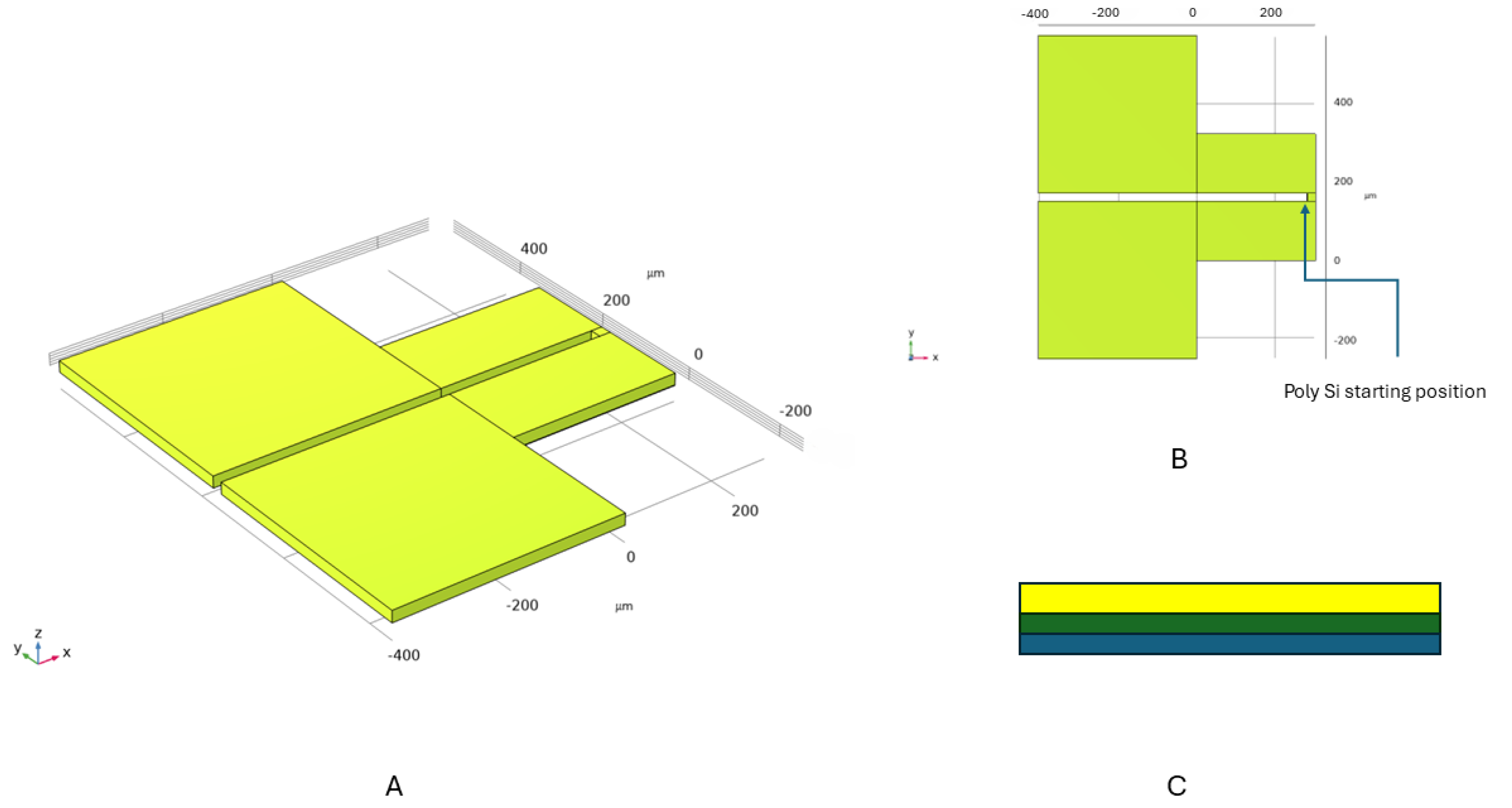
3.1. Basic Design
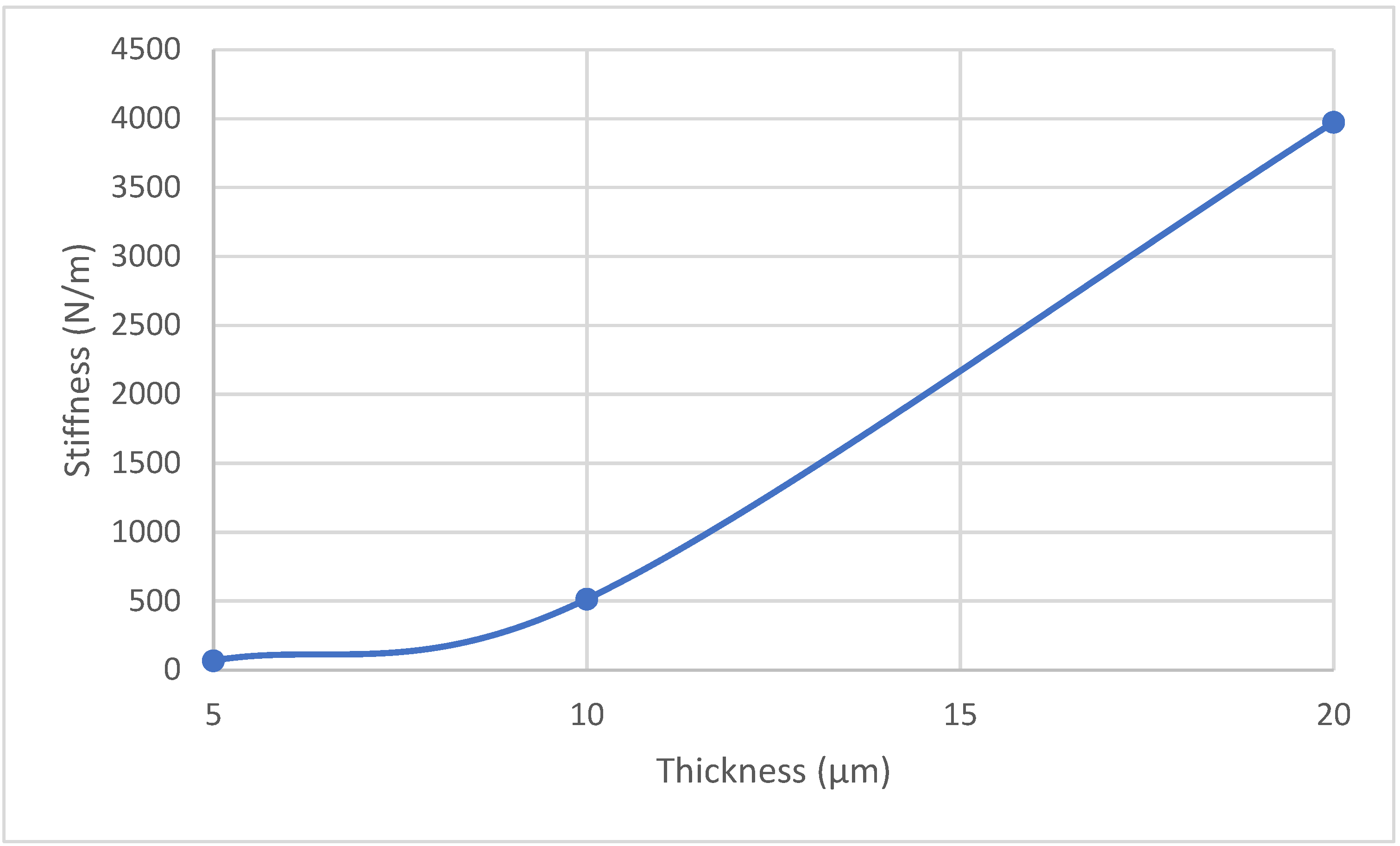
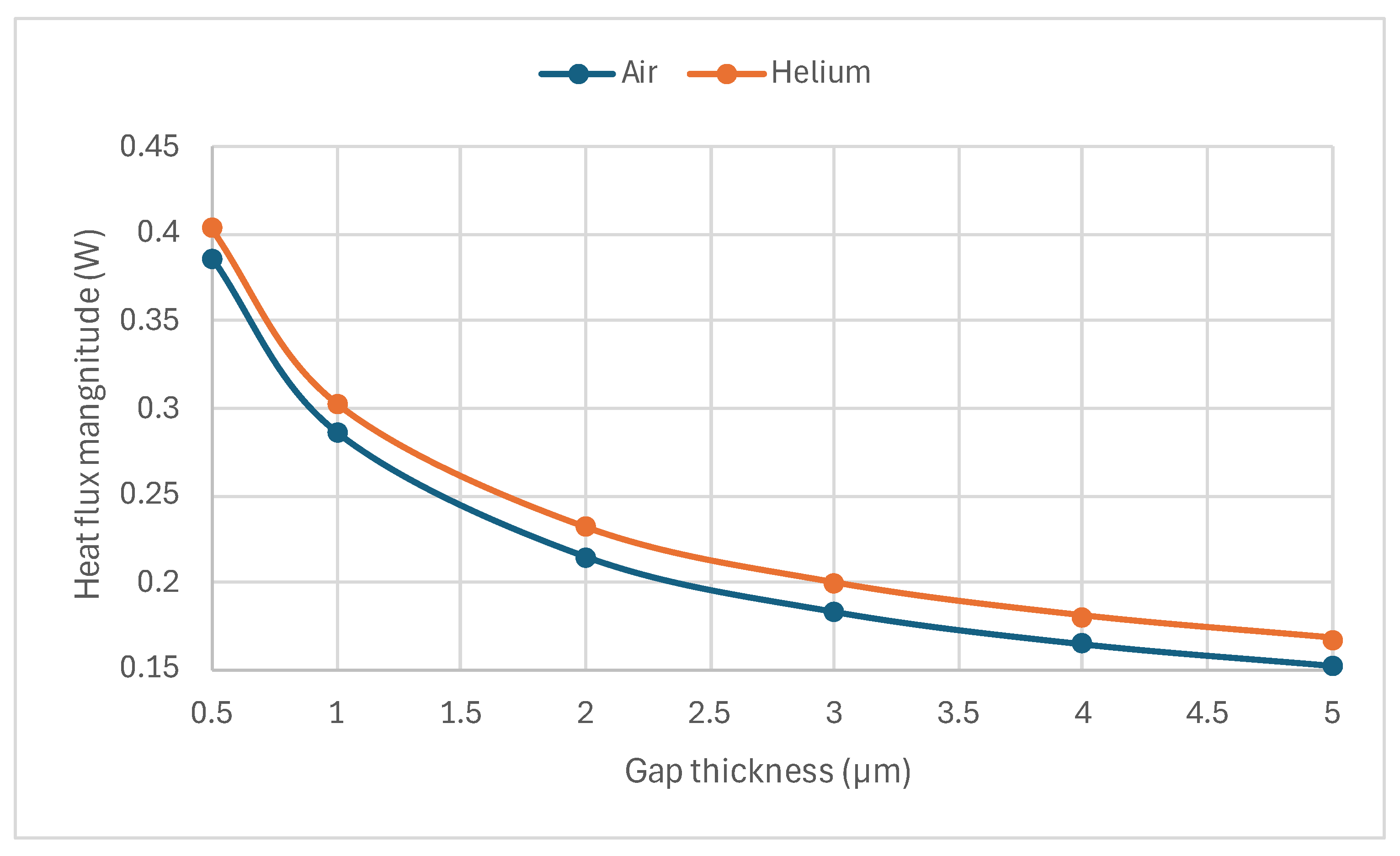
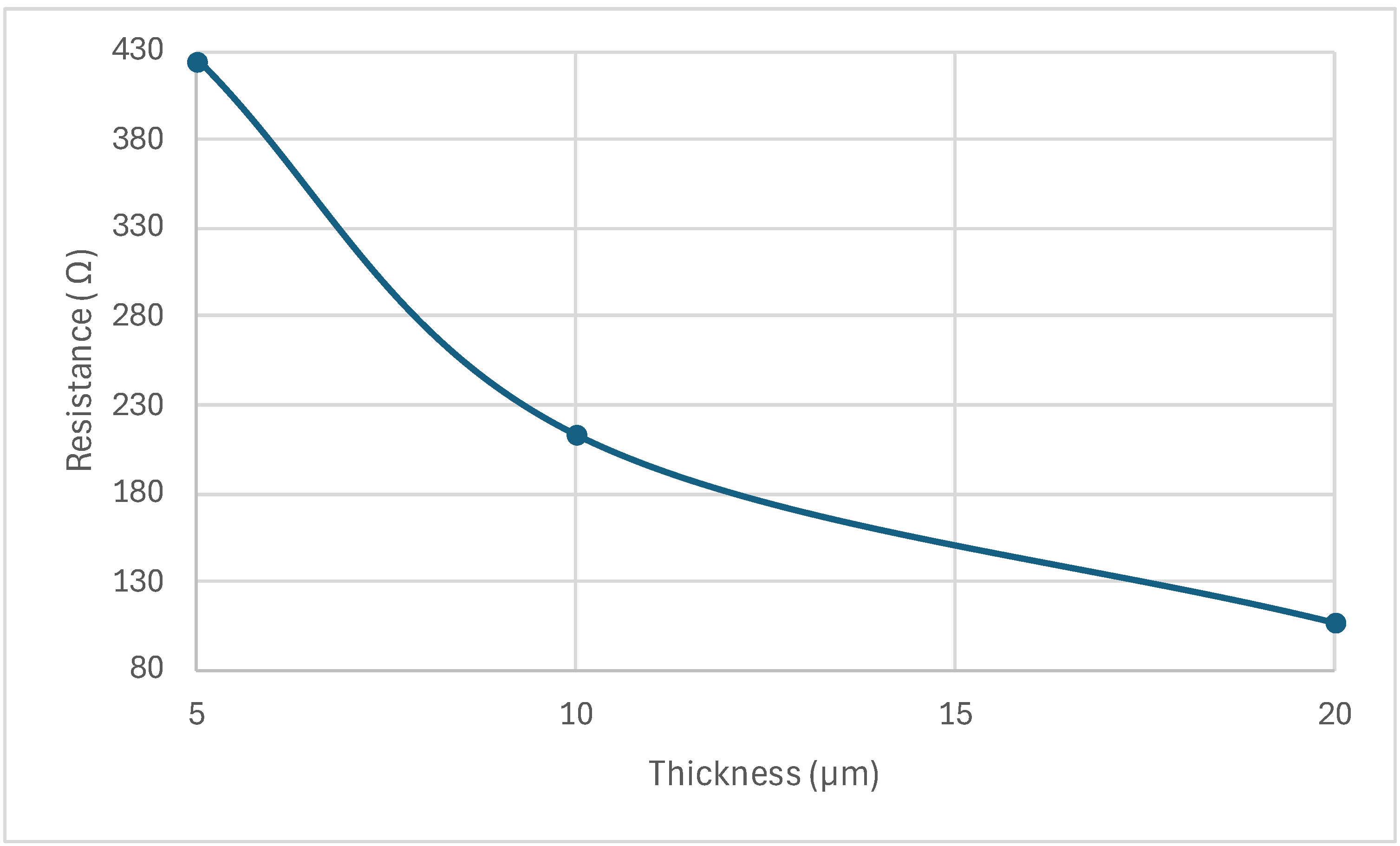
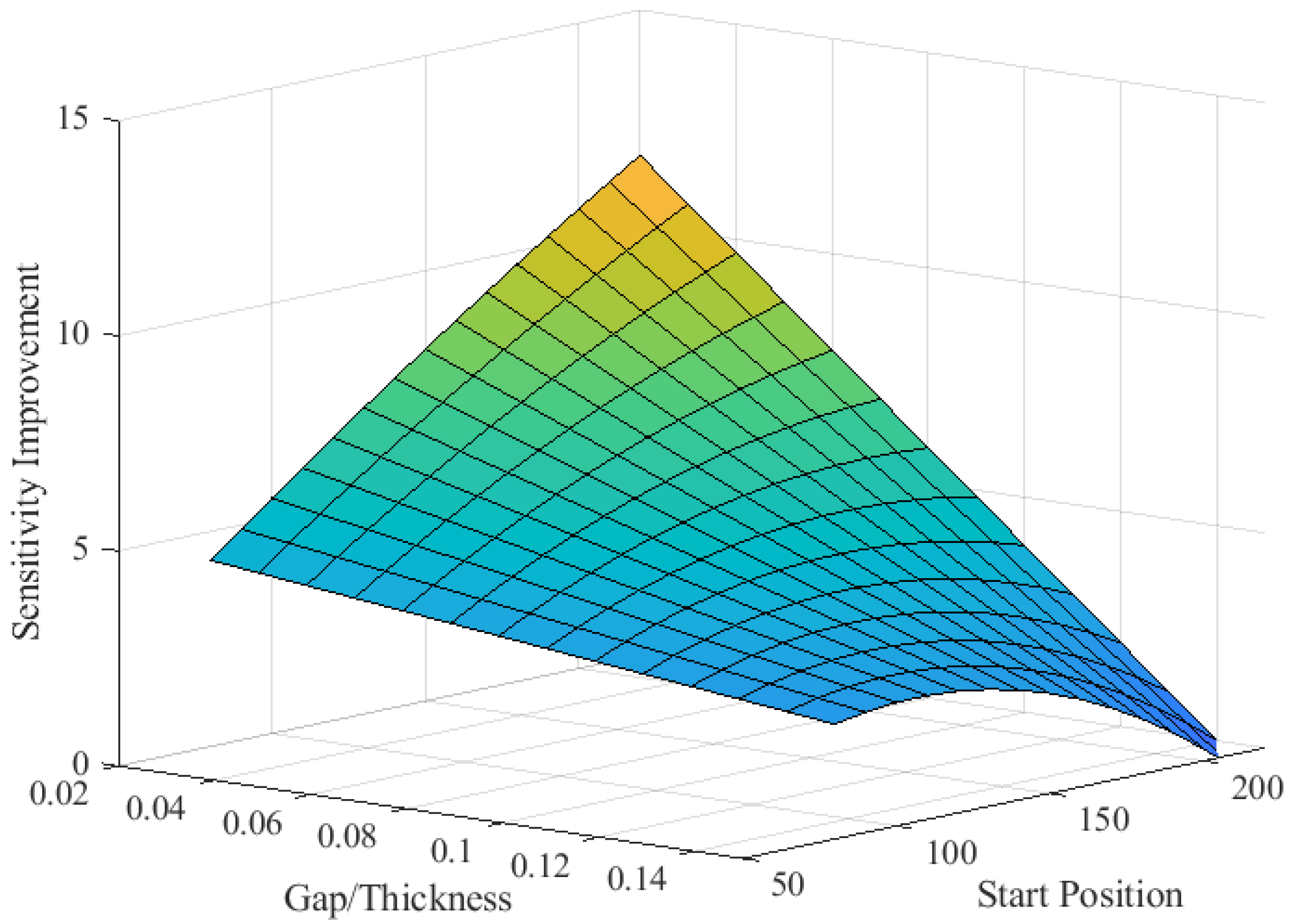
3.2. Geometry Effect
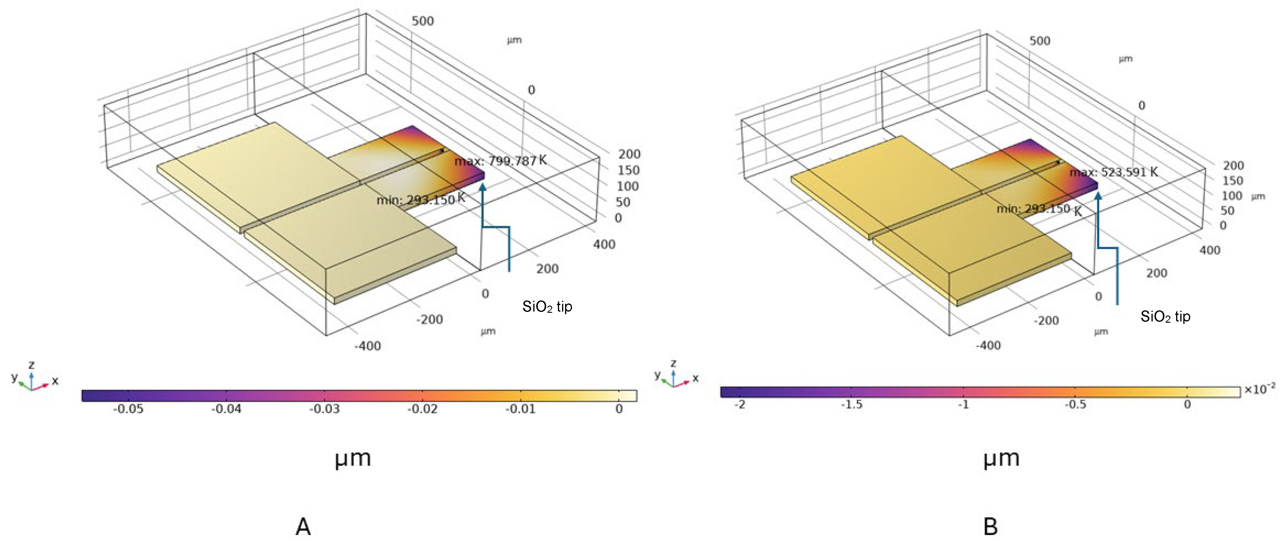
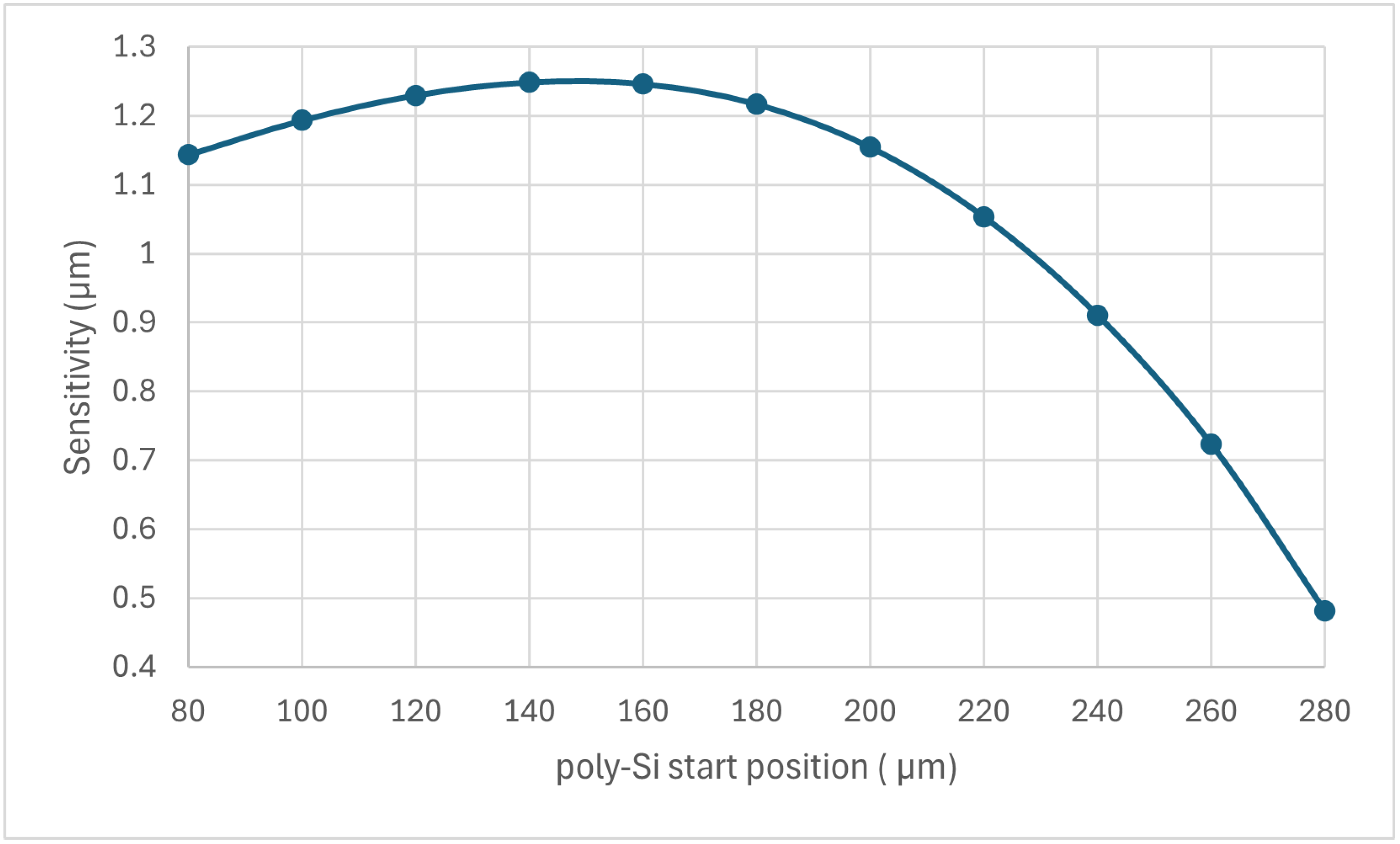
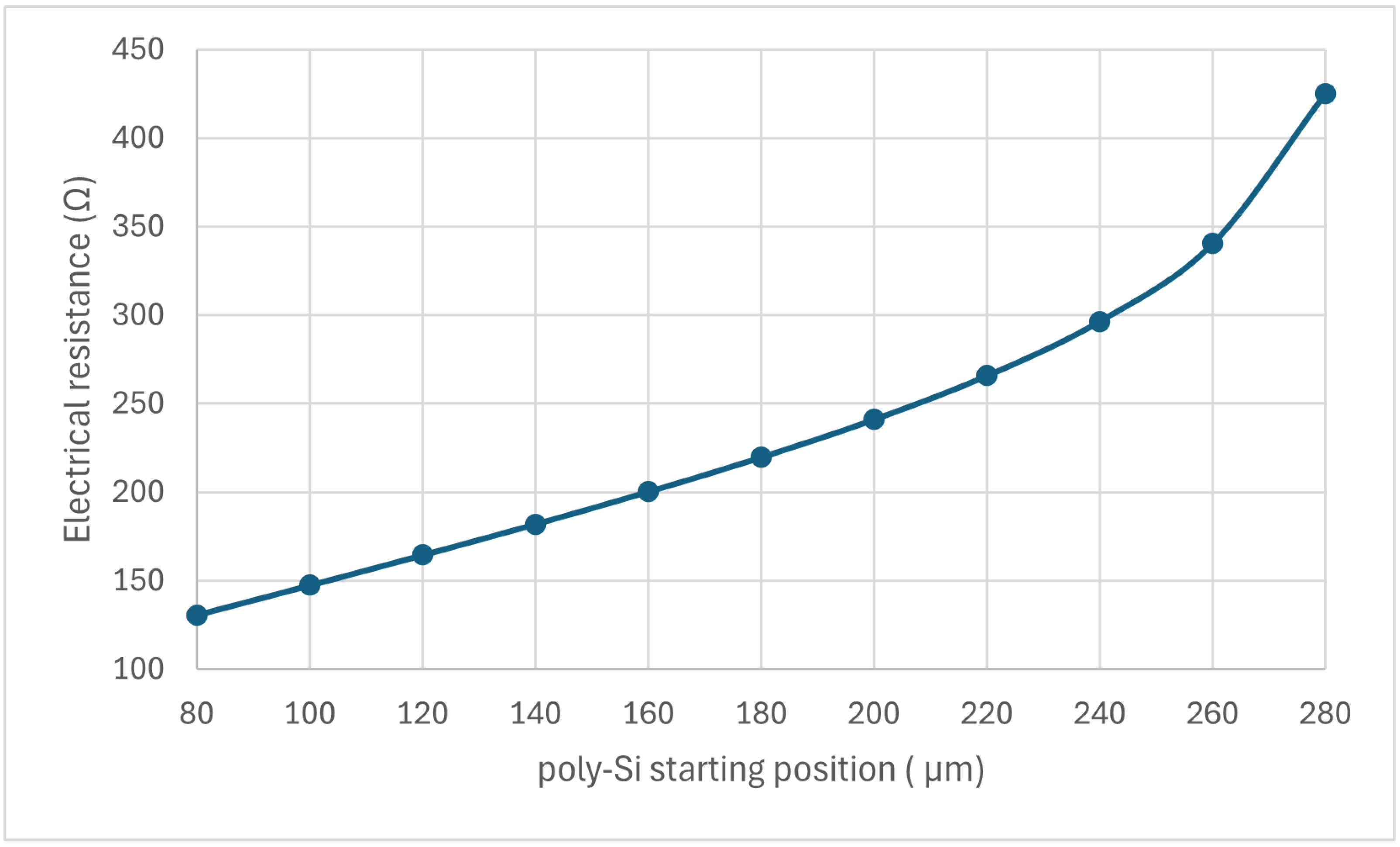
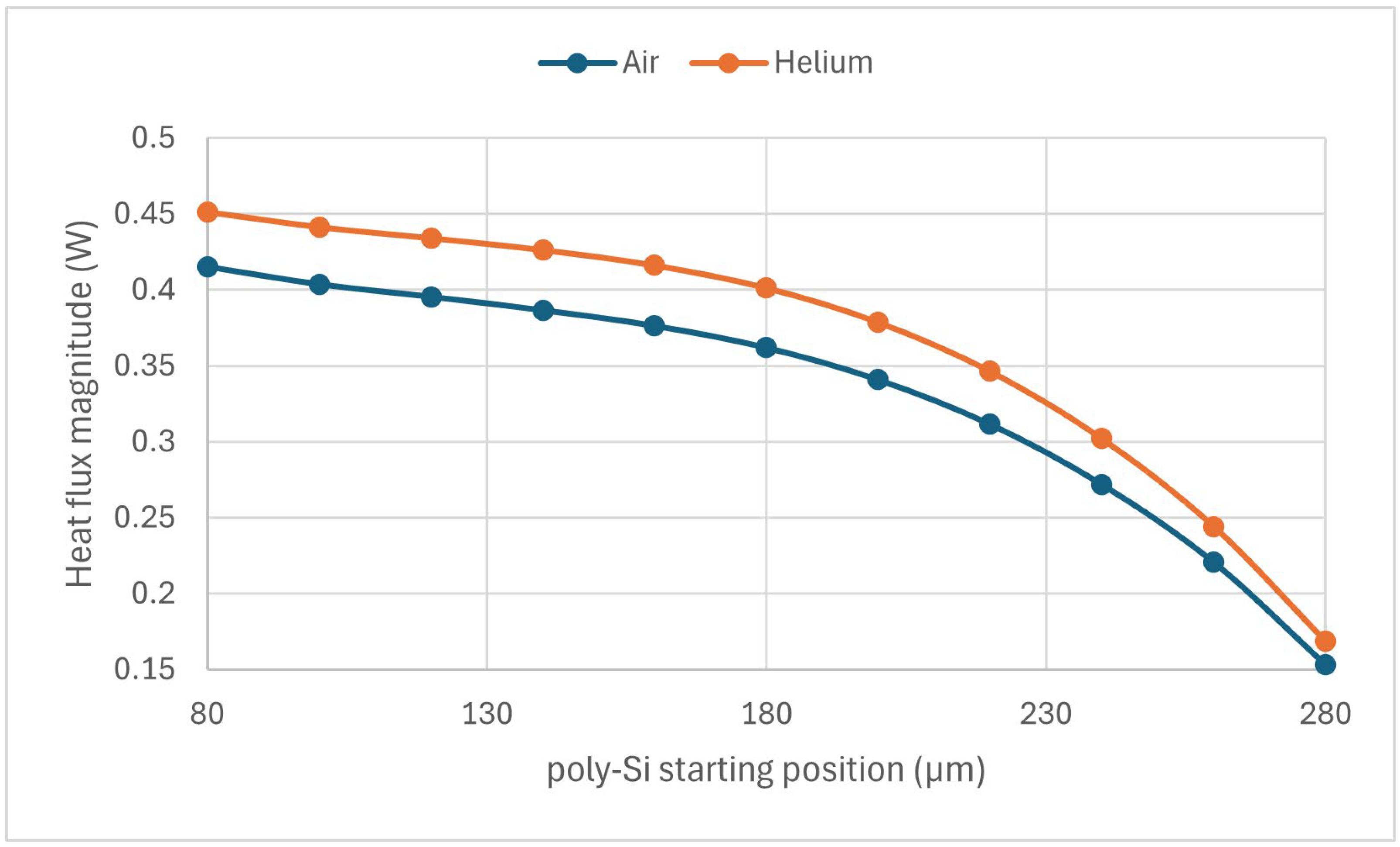
3.3. Effect of the Trench
3.4. Effect of the SiO2 Layer Thickness and Location
4. Discussion
- Construct a nonlinear equation that fits the relationship between the trench and the sensitivity
- Divide the Equation by the beam thickness
- Multiply the Equation by the gap distance
5. Conclusions
Author Contributions
Funding
Institutional Review Board Statement
Informed Consent Statement
Data Availability Statement
Conflicts of Interest
References
- Angelucci, M.; Herranz, L.E.; Paci, S. On the behavior of a concrete-based dry cask for spent nuclear fuel in off-normal and accidental conditions. Nucl. Eng. Des. 2024, 419, 112992. [Google Scholar] [CrossRef]
- Algamili, A.S.; Khir, M.H.; Dennis, J.O.; Ahmed, A.Y.; Alabsi, S.S.; Ba Hashwan, S.S.; Junaid, M.M. A review of actuation and sensing mechanisms in MEMS-based sensor devices. Nanoscale Res. Lett. 2021, 16, 16. [Google Scholar] [CrossRef] [PubMed]
- Asri, M.I.; Hasan, M.N.; Fuaad, M.R.; Yunos, Y.M.; Ali, M.S. MEMS gas sensors: A review. IEEE Sens. J. 2021, 21, 18381–18397. [Google Scholar] [CrossRef]
- Berndt, D.; Muggli, J.; Wittwer, F.; Langer, C.; Heinrich, S.; Knittel, T.; Schreiner, R. MEMS-based thermal conductivity sensor for hydrogen gas detection in automotive applications. Sens. Actuators A Phys. 2020, 305, 111670. [Google Scholar] [CrossRef]
- Gardner, E.L.; Gardner, J.W.; Udrea, F. Micromachined thermal gas sensors—A review. Sensors 2023, 23, 681. [Google Scholar] [CrossRef] [PubMed]
- Xie, D.; Zhang, Y.; He, D.; Yang, Y.; Liu, R.; Xing, C.; Chen, D.; Geng, L.; Wu, Q.; Yao, D.; et al. A High Heat Transfer Efficiency MEMS Thermal Conductivity Gas Sensor with Bridge Structure for Hydrogen Detection. In Proceedings of the 2024 IEEE 37th International Conference on Micro Electro Mechanical Systems (MEMS), Austin, TX, USA, 21–25 January 2024; IEEE: Piscataway, NJ, USA, 2024; pp. 879–882. [Google Scholar]
- Samotaev, N.; Podlepetsky, B.; Mashinin, M.; Ivanov, I.; Obraztsov, I.; Oblov, K.; Dzhumaev, P. Thermal Conductivity Gas Sensors for High-Temperature Applications. Micromachines 2024, 15, 138. [Google Scholar] [CrossRef] [PubMed]
- Lee, H. Thermal Design: Heat Sinks, Thermoelectrics, Heat Pipes, Compact Heat Exchangers, and Solar Cells; John Wiley & Sons: Hoboken, NJ, USA, 2022. [Google Scholar]
- Potekhina, A.; Wang, C. Review of electrothermal actuators and applications. Actuators 2019, 8, 69. [Google Scholar] [CrossRef]
- Chen, B.; Wu, X.; Peng, X. Finite element analysis of ring strain sensor. Sens. Actuators A Phys. 2007, 139, 66–69. [Google Scholar] [CrossRef]
- Singh, K.; Alvi, P.A. Finite element analysis of polysilicon-based MEMS temperature-pressure sensor. Mater. Today Proc. 2020, 27, 280–283. [Google Scholar]
- Sciberras, T.; Demicoli, M.; Grech, I.; Mallia, B.; Mollicone, P.; Sammut, N. Coupled finite element-finite volume multiphysics analysis of MEMS electrothermal actuators. Micromachines 2021, 13, 8. [Google Scholar] [CrossRef] [PubMed]
- Dickinson, E.J.; Ekström, H.; Fontes, E. COMSOL Multiphysics®: Finite element software for electrochemical analysis. Mini-Rev. Electrochem. Commun. 2014, 40, 71–74. [Google Scholar] [CrossRef]
- Shi, T.; Xu, H.; Qi, C.; Lei, B.; Wu, Y.; Zhao, C. Multiphysics modeling of thermochemical heat storage with enhance heat transfer. Appl. Therm. Eng. 2021, 198, 117508. [Google Scholar] [CrossRef]
- Bayat, M.; Dong, W.; Thorborg, J.; To, A.C.; Hattel, J.H. A review of multi-scale and multiphysics simulations of metal additive manufacturing processes with focus on modeling strategies. Addit. Manuf. 2021, 47, 102278. [Google Scholar]
- Sun, J.; Zhang, G.; Zhao, Y. Design of a multiphysics coupling MEMS pressure sensor. J. Phys. Conf. Ser. 2024, 2740, 012045. [Google Scholar] [CrossRef]
- Xu, H.; Wang, Z.; Zhou, Z.; Yi, Z.; Qin, M.; Huang, Q.A. An efficient macromodel extraction strategy for packaged MEMS thermal wind sensor considering multiphysics. IEEE Sens. J. 2023, 23, 5879–5891. [Google Scholar] [CrossRef]
- Alrashed, H.; Obeid, A.; Albrithen, H.; Muthuramamoorthy, M.; Rahman, S.; Al-Gawati, M.A.; Alodhayb, A.N. Modeling the mechanical response of microelectromechanical system (MEMS)-based sensors to volatile alcohol vapors: A finite element analysis. AIP Adv. 2024, 14, 035034. [Google Scholar] [CrossRef]
- Guo, X.; Li, M.; Li, L.; Liu, P.; Zhao, C.; Liu, Z. Study on poly-silicon resistivity control with nano-scale grain size. In Proceedings of the 2013 13th IEEE International Conference on Nanotechnology (IEEE-NANO 2013), Beijing, China, 5–8 August 2013; IEEE: Piscataway, NJ, USA, 2013; pp. 950–953. [Google Scholar]
- Mahdavifar, A.; Aguilar, R.; Peng, Z.; Hesketh, P.J.; Findlay, M.; Stetter, J.R.; Hunter, G.W. Simulation and fabrication of an ultra-low power miniature microbridge thermal conductivity gas sensor. J. Electrochem. Soc. 2014, 161, B55. [Google Scholar] [CrossRef]
- Oh, C.S.; Coles, G.; Sharpe, W.N. High temperature behavior of poly-silicon. In MRS Online Proceedings Library (OPL); Springer: Berlin/Heidelberg, Germany, 2002; p. 741. [Google Scholar]
- Incropera, F.P.; DeWitt, D.P.; Bergman, T.L.; Lavine, A.S. Fundamentals of Heat and Mass Transfer; Wiley: New York, NY, USA, 2017. [Google Scholar]
- Hubert, C.; André, D.; Dubar, L.; Iordanoff, I.; Charles, J.L. Simulation of continuum electrical conduction and Joule heating using DEM domains. Int. J. Numer. Methods Eng. 2017, 110, 862–877. [Google Scholar] [CrossRef]
- Hasan, M.H.; Alsaleem, F.; Ramini, A. Voltage and Deflection Amplification via Double Resonance Excitation in a Cantilever Microstructure. Sensors 2019, 19, 380. [Google Scholar] [CrossRef]
- Hajjaj, A.; Jaber, N.; Alcheikh, N.; Younis, M. A Resonant Gas Sensor Based on Multimode Excitation of a Buckled Microbeam. IEEE Sens. J. 2020, 20, 1778–1785. [Google Scholar] [CrossRef]
- Mohaidat, S.; Alsaleem, F. A Threshold Helium Leakage Detection Switch with Ultra Low Power Operation. Sensors 2023, 23, 4019. [Google Scholar] [CrossRef]


| Beam Thickness (µm) | Gap Thickness (µm) | Input Voltage (V) |
|---|---|---|
| 5 | 0.5 | 13.234 |
| 5 | 1.0 | 11.504 |
| 5 | 2.0 | 10.105 |
| 5 | 3.0 | 9.418 |
| 5 | 4.0 | 8.989 |
| 5 | 5.0 | 8.688 |
| 10 | 0.5 | 11.365 |
| 10 | 1.0 | 9.991 |
| 10 | 2.0 | 8.875 |
| 10 | 3.0 | 8.347 |
| 10 | 4.0 | 8.027 |
| 10 | 5.0 | 7.809 |
| 20 | 0.5 | 9.896 |
| 20 | 1.0 | 8.807 |
| 20 | 2.0 | 7.96 |
| 20 | 3.0 | 7.583 |
| 20 | 4.0 | 7.365 |
| 20 | 5.0 | 7.221 |
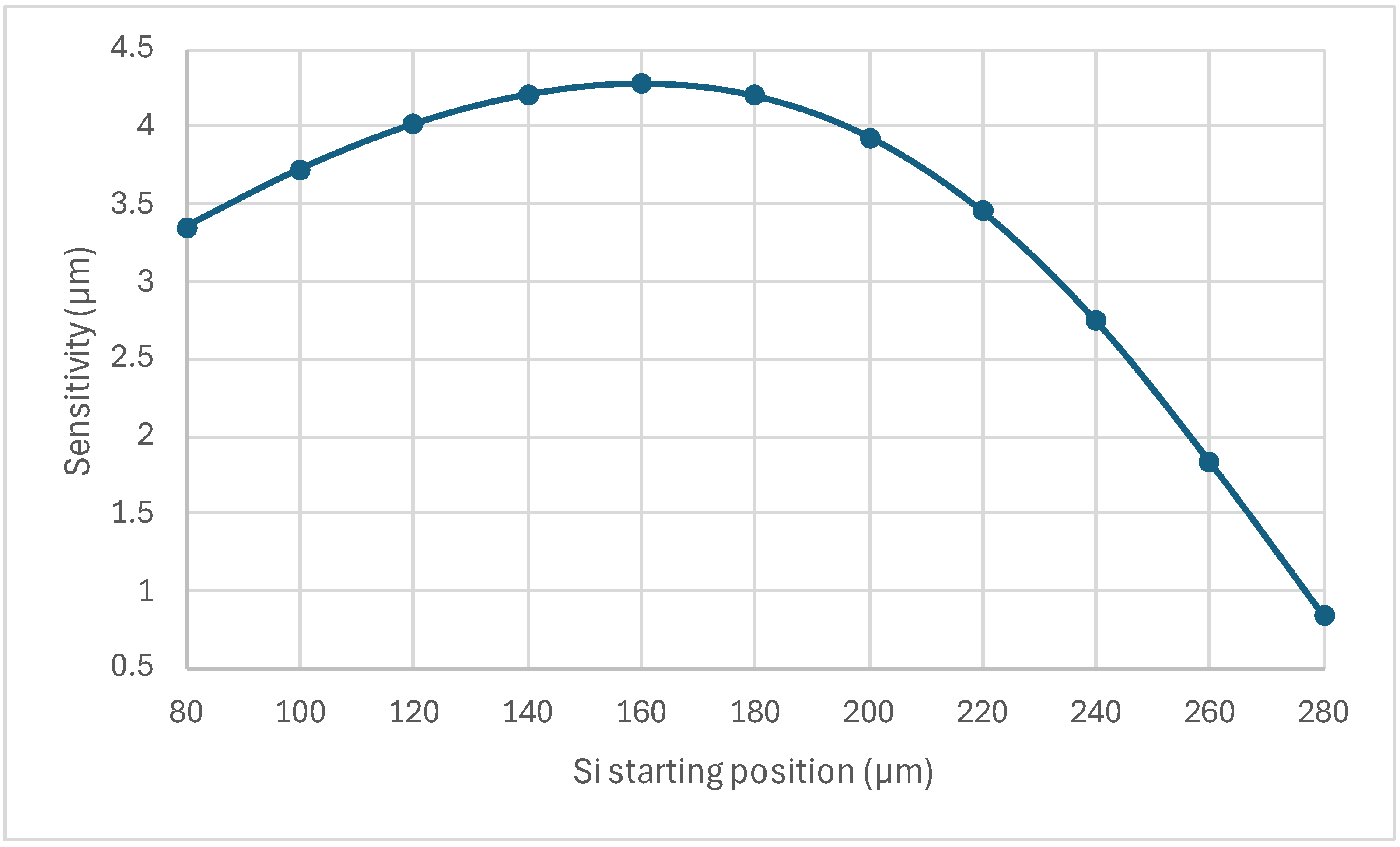
| Si Start Position (µm) | Input Voltage (V) |
|---|---|
| 80 | 8.16 |
| 100 | 8.537 |
| 120 | 8.904 |
| 140 | 9.248 |
| 160 | 9.553 |
| 180 | 9.975 |
| 200 | 9.941 |
| 220 | 9.953 |
| 240 | 9.789 |
| 260 | 9.399 |
| 280 | 8.688 |
| Helium Volume Fraction | Displacement (µm) | Displacement Difference (µm) |
|---|---|---|
| 0 | 5.30 | 0 |
| 0.01 | 5.11 | 0.19 |
| 0.02 | 4.92 | 0.19 |
| 0.03 | 4.75 | 0.17 |
| 0.04 | 4.59 | 0.16 |
| 0.05 | 4.44 | 0.15 |
Disclaimer/Publisher’s Note: The statements, opinions and data contained in all publications are solely those of the individual author(s) and contributor(s) and not of MDPI and/or the editor(s). MDPI and/or the editor(s) disclaim responsibility for any injury to people or property resulting from any ideas, methods, instructions or products referred to in the content. |
© 2024 by the authors. Licensee MDPI, Basel, Switzerland. This article is an open access article distributed under the terms and conditions of the Creative Commons Attribution (CC BY) license (https://creativecommons.org/licenses/by/4.0/).
Share and Cite
Mohaidat, S.; Alsaleem, F. Modeling and Design Parameter Optimization to Improve the Sensitivity of a Bimorph Polysilicon-Based MEMS Sensor for Helium Detection. Sensors 2024, 24, 3626. https://doi.org/10.3390/s24113626
Mohaidat S, Alsaleem F. Modeling and Design Parameter Optimization to Improve the Sensitivity of a Bimorph Polysilicon-Based MEMS Sensor for Helium Detection. Sensors. 2024; 24(11):3626. https://doi.org/10.3390/s24113626
Chicago/Turabian StyleMohaidat, Sulaiman, and Fadi Alsaleem. 2024. "Modeling and Design Parameter Optimization to Improve the Sensitivity of a Bimorph Polysilicon-Based MEMS Sensor for Helium Detection" Sensors 24, no. 11: 3626. https://doi.org/10.3390/s24113626