
Detecting Near-Surface Sub-Millimeter Voids in Additively Manufactured Ti-5V-5Al-5Mo-3Cr Alloy Using a Transmit-Receive Eddy Current Probe
 ,
, 
Abstract
1. Introduction
1.1. Background and Motivation
1.2. Theory
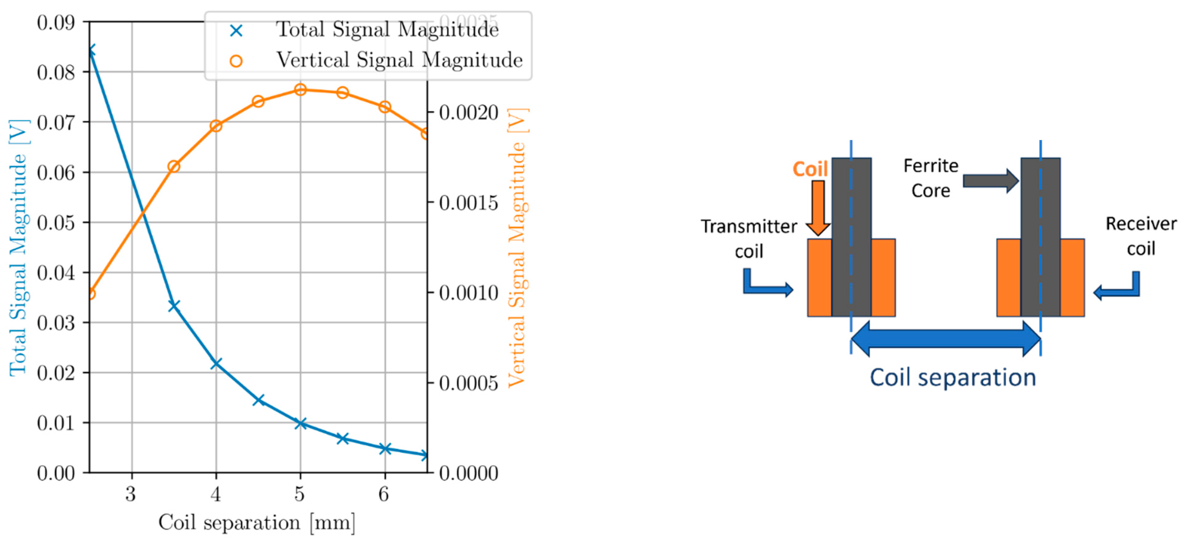
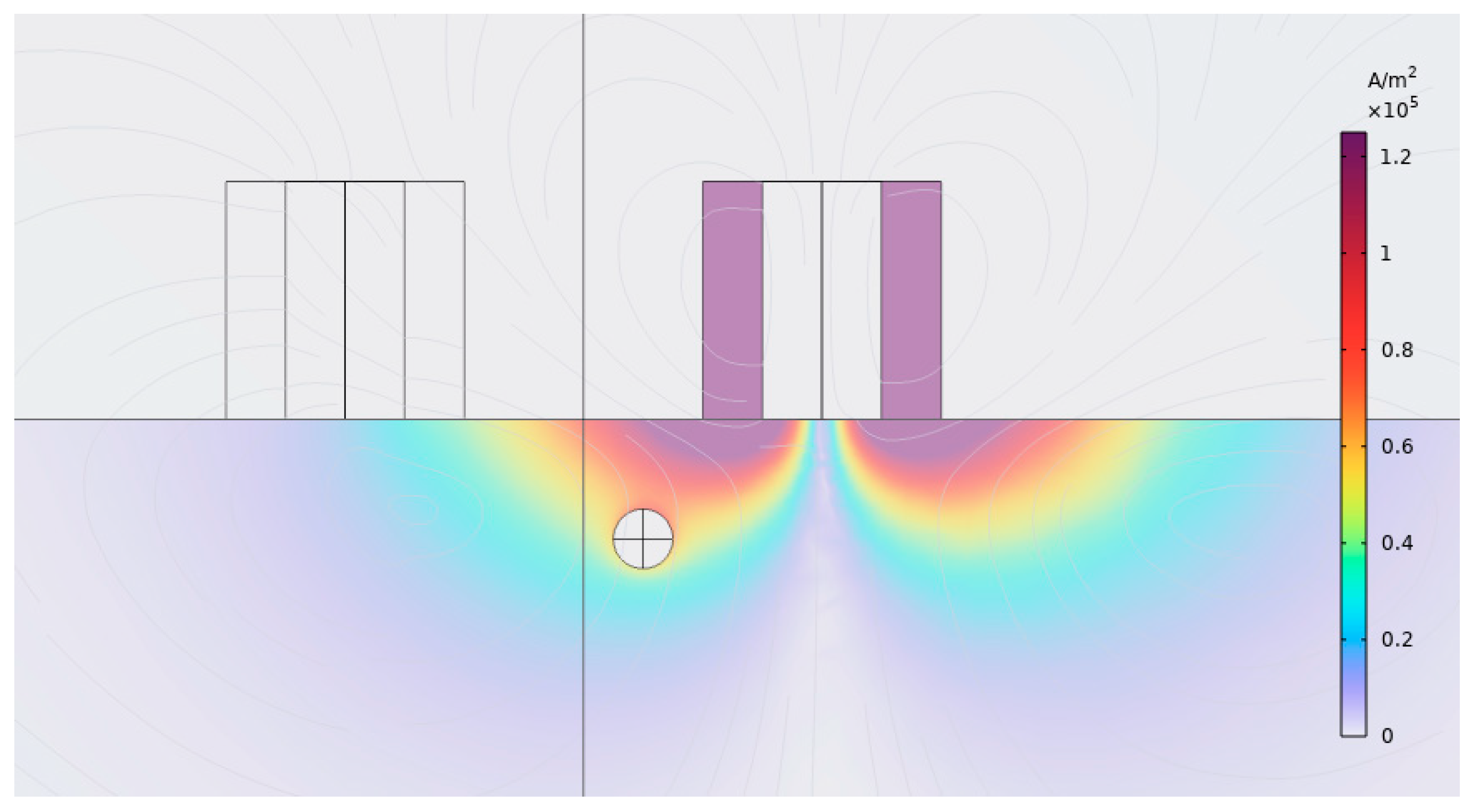
1.3. Finite Element Modelling
2. Experimental Technique
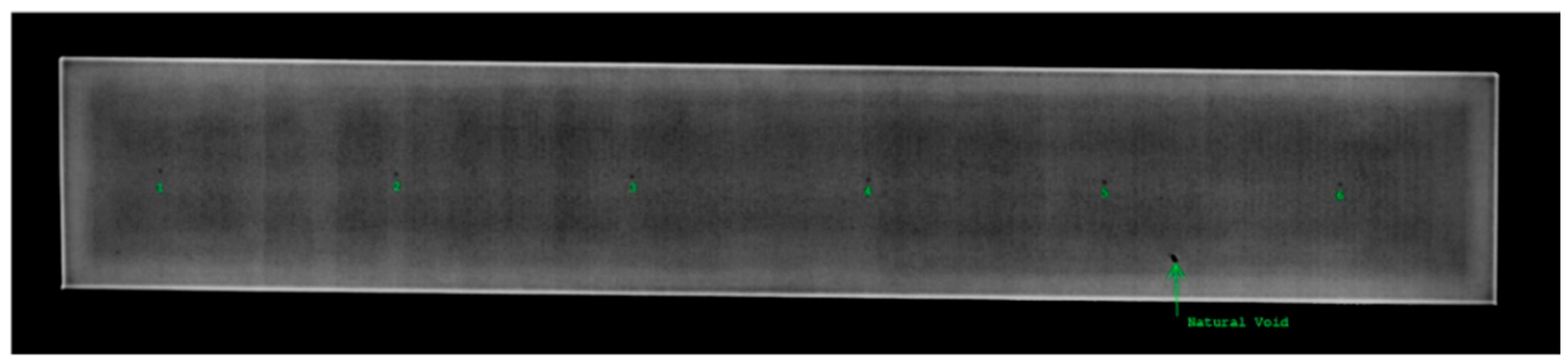
2.1. Materials
2.2. Probe
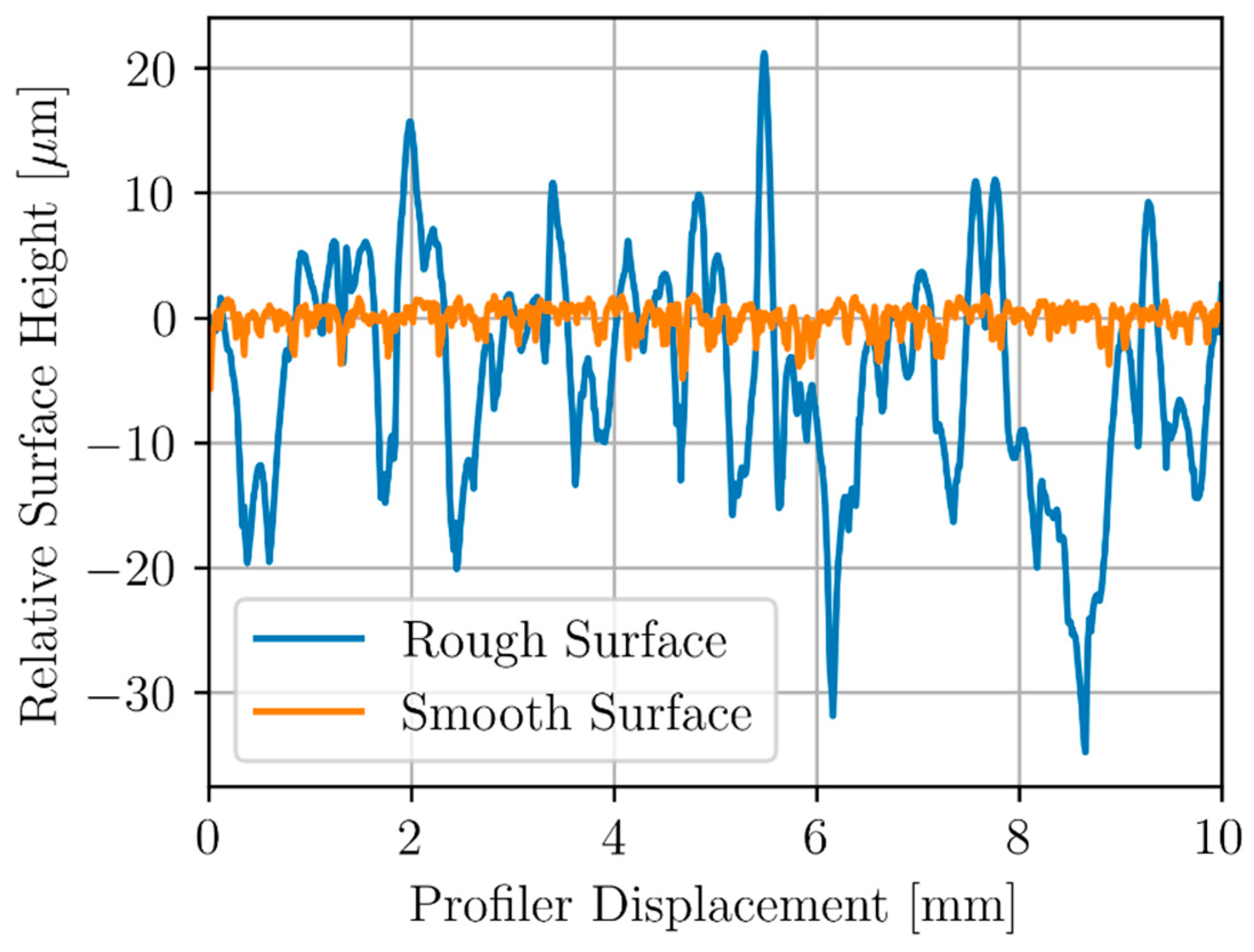
2.3. Apparatus
3. Results and Discussion
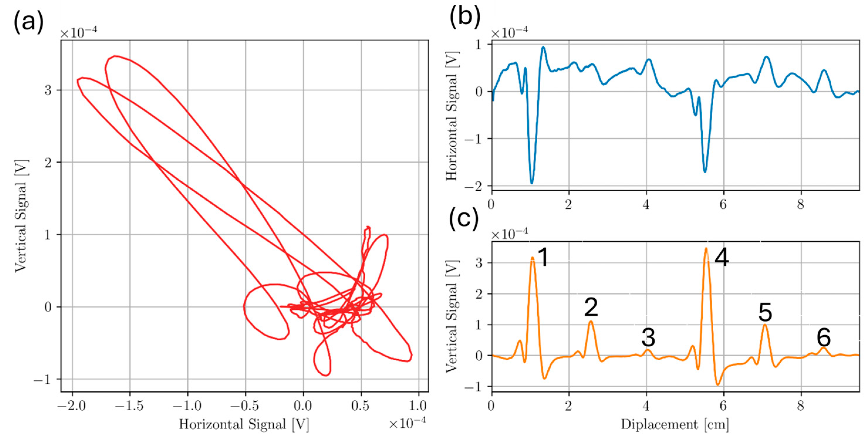
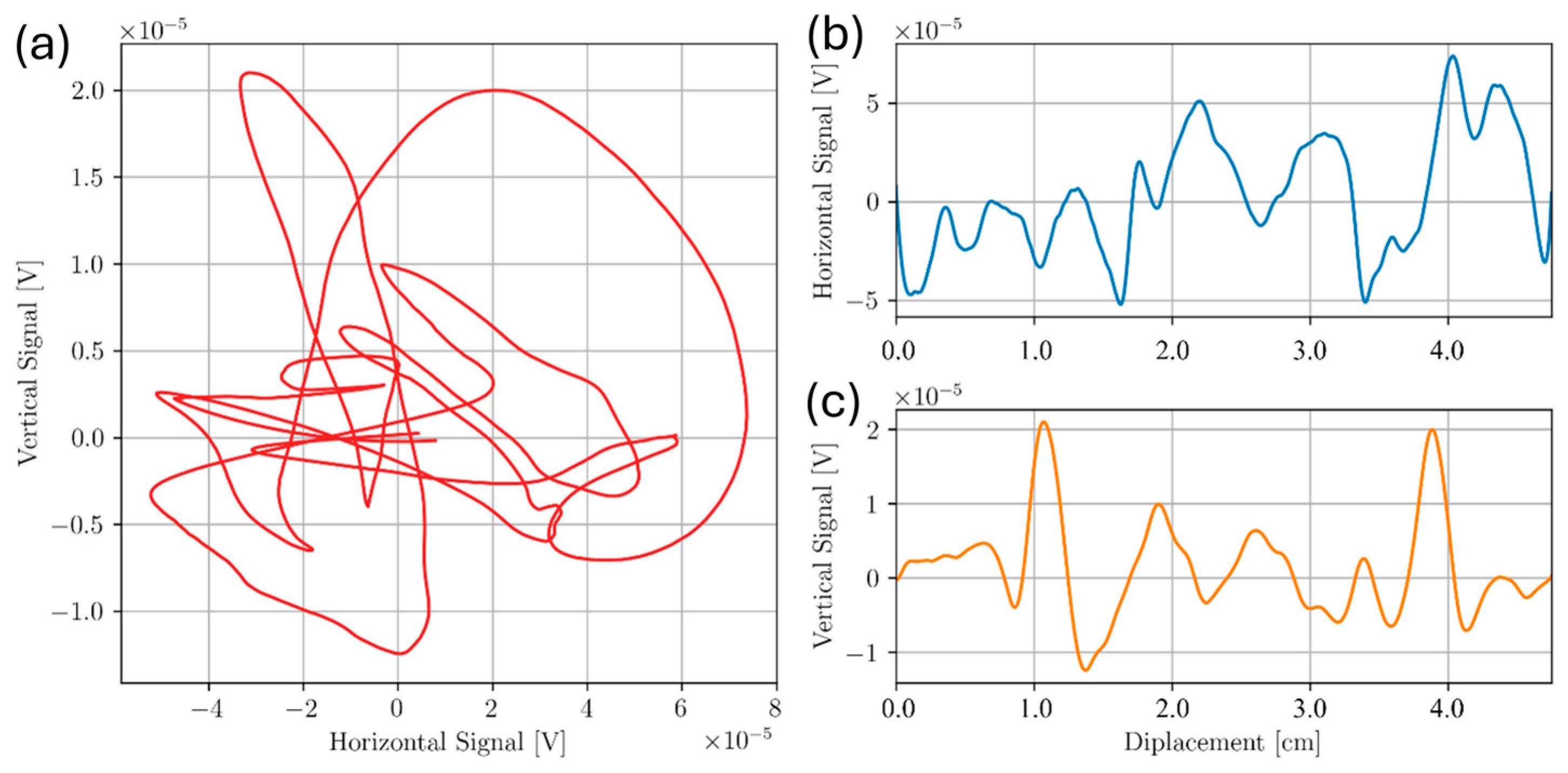
3.1. Sample D
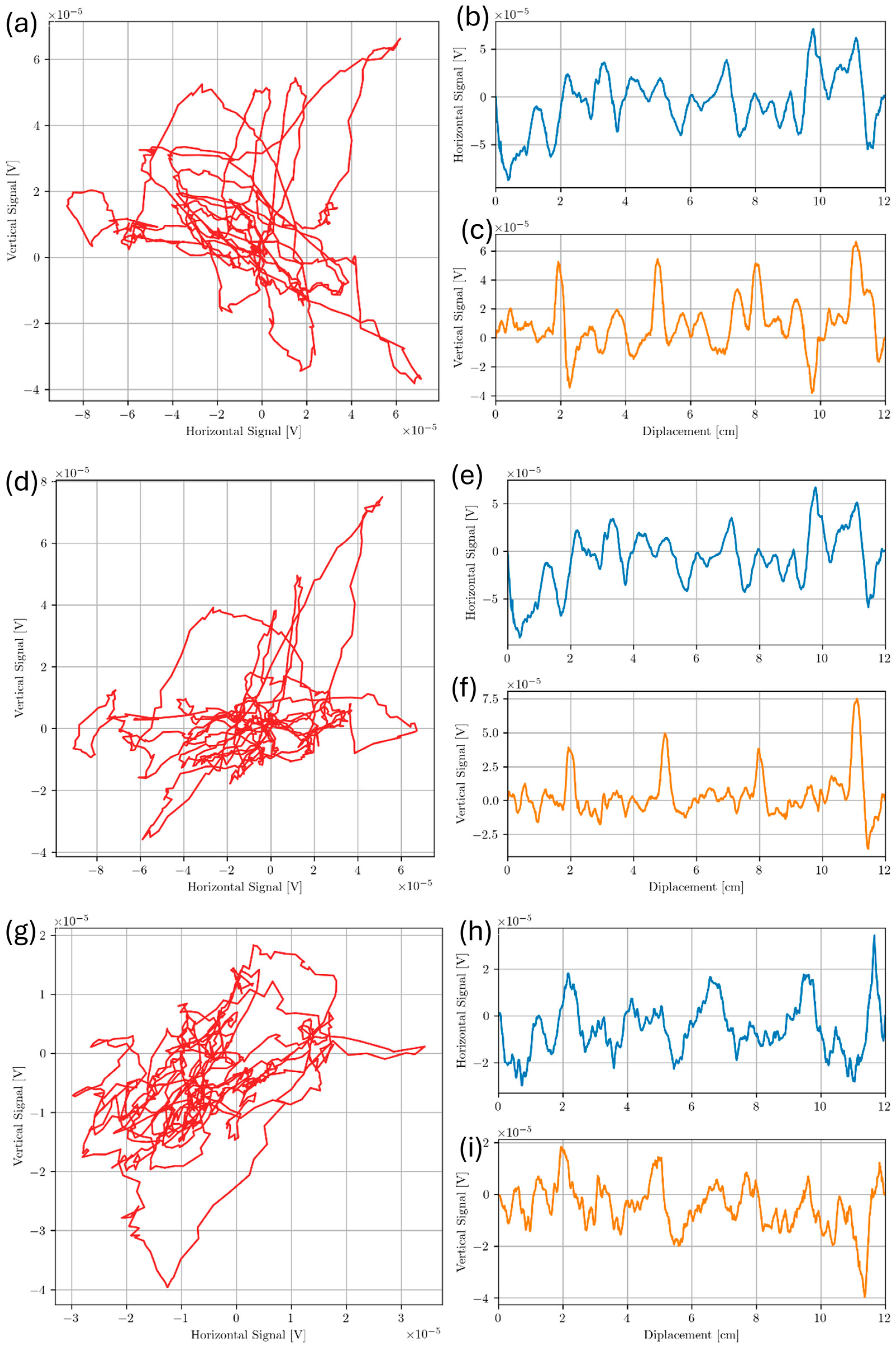
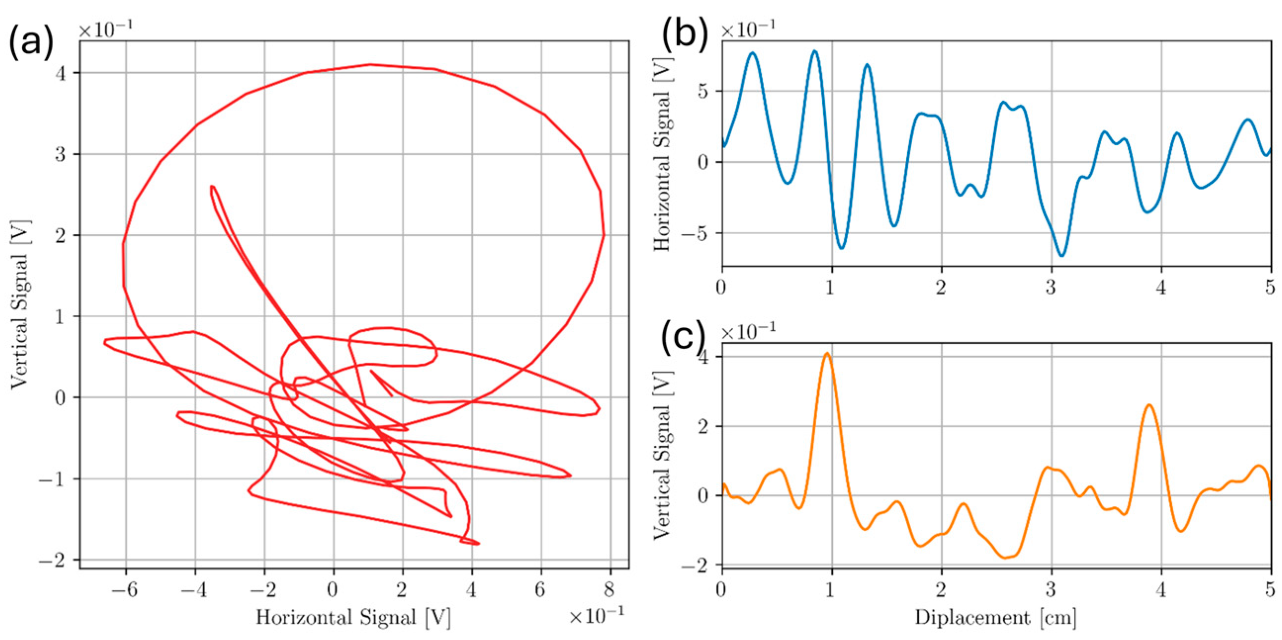
3.2. Sample A
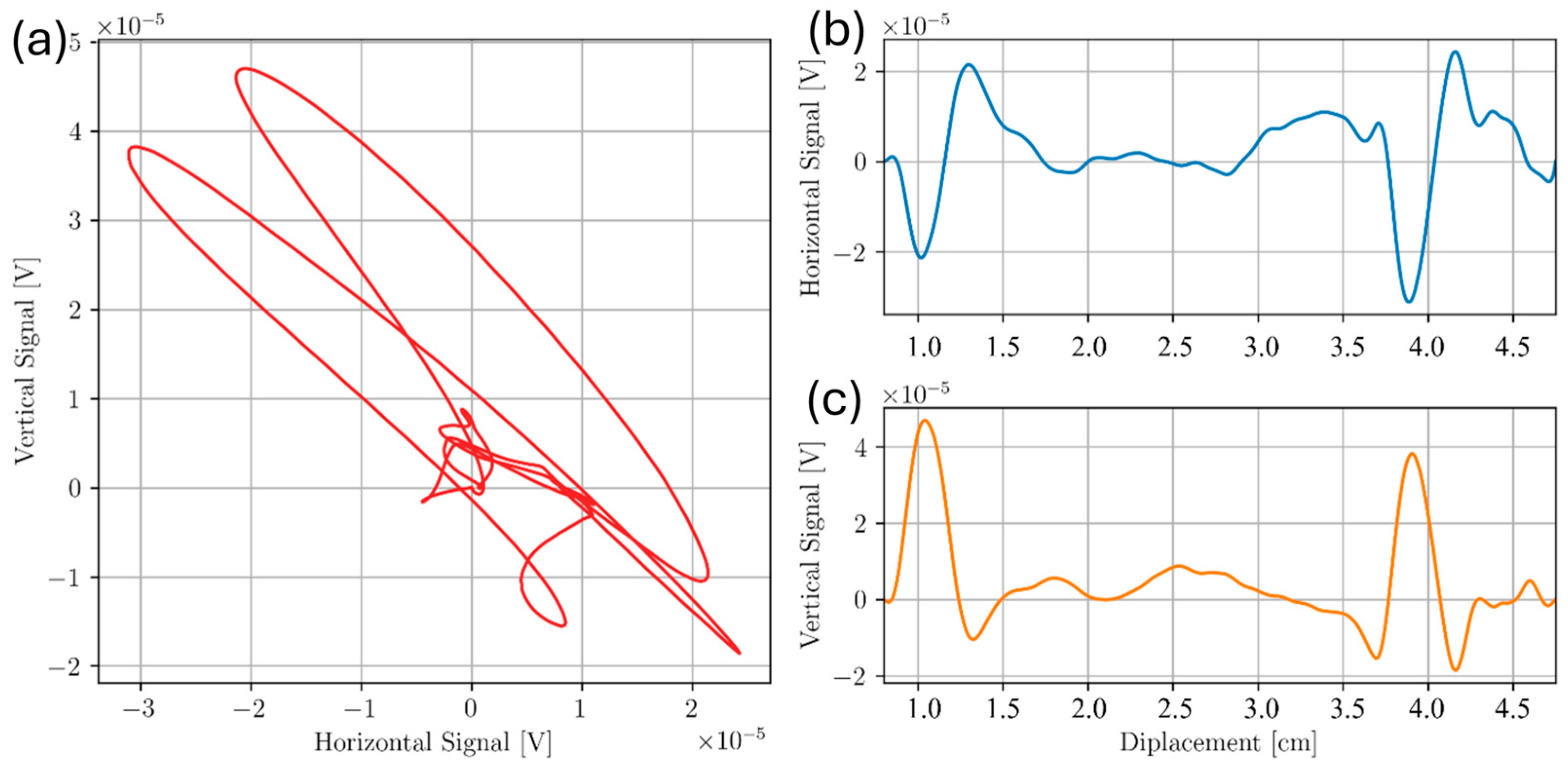
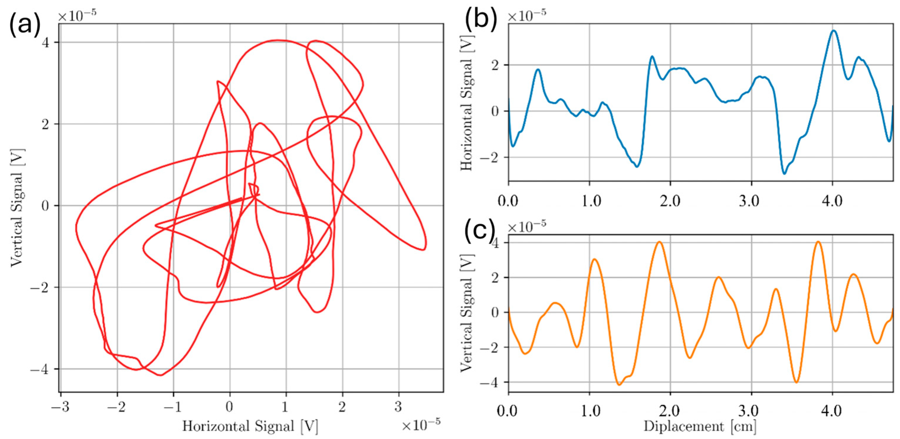
3.3. Sample C
4. Conclusions
Author Contributions
Funding
Institutional Review Board Statement
Informed Consent Statement
Data Availability Statement
Acknowledgments
Conflicts of Interest
References
- El Cheikh, H.; Courant, B.; Branchu, S.; Huang, X.; Hascot, J.Y.; Guilln, R. Direct Laser Fabrication process with coaxial powder projection of 316L steel. Geometrical characteristics and microstructure characterization of wall structures. Opt. Lasers Eng. 2012, 50, 1779–1784. [Google Scholar] [CrossRef]
- Rebecca, L. Additive Manufacturing, Explained|MIT Sloan. Available online: https://mitsloan.mit.edu/ideas-made-to-matter/additive-manufacturing-explained (accessed on 17 March 2024).
- Nyamekye, P.; Leino, M.; Piili, H.; Salminen, A. Overview of Sustainability Studies of CNC Machining and LAM of Stainless Steel. Phys. Procedia 2015, 78, 367–376. [Google Scholar] [CrossRef]
- Rinaldi, M.; Caterino, M.; Manco, P.; Fera, M.; Macchiaroli, R. The impact of Additive Manufacturing on Supply Chain design: A simulation study. Procedia Comput. Sci. 2021, 180, 446–455. [Google Scholar] [CrossRef]
- Jeon, T.J.; Hwang, T.W.; Yun, H.J.; VanTyne, C.J.; Moon, Y.H. Control of Porosity in Parts Produced by a Direct Laser Melting Process. Appl. Sci. 2018, 8, 2573. [Google Scholar] [CrossRef]
- Razavi, S.M.J.; Bordonaro, G.G.; Ferro, P.; Torgersen, J.; Berto, F. Fatigue Behavior of Porous Ti-6Al-4V Made by Laser-Engineered Net Shaping. Materials 2018, 11, 284. [Google Scholar] [CrossRef] [PubMed]
- Liu, M.; Kumar, A.; Bukkapatnam, S.; Kuttolamadom, M. A Review of the Anomalies in Directed Energy Deposition (DED) Processes & Potential Solutions—Part Quality & Defects. Procedia Manuf. 2021, 53, 507–518. [Google Scholar] [CrossRef]
- Jarfors, A.E.W.; Matsushita, T.; Siafakas, D.; Stolt, R. On the nature of the anisotropy of Maraging steel (1.2709) in additive manufacturing through powder bed laser-based fusion processing. Mater. Des. 2021, 204, 109608. [Google Scholar] [CrossRef]
- Benstock, D.; Cegla, F.; Stone, M. The influence of surface roughness on ultrasonic thickness measurements. J. Acoust. Soc. Am. 2014, 136, 3028–3039. [Google Scholar] [CrossRef]
- Huang, Y.; Turner, J.A.; Song, Y.; Ni, P.; Li, X. Enhanced ultrasonic detection of near-surface flaws using transverse-wave backscatter. Ultrasonics 2019, 98, 20–27. [Google Scholar] [CrossRef]
- Xu, Z.; Tian, Q.; Hu, P.; Li, H.; Shen, S. Laser ultrasonic detection of submillimeter artificial holes in laser powder bed fusion manufactured alloys. Opt. Laser Technol. 2024, 169, 110030. [Google Scholar] [CrossRef]
- Zuljan, D.; Zhou, Z. Effect of ultrasonic coupling media and surface roughness on contact transfer loss. Cogent Eng. 2022, 9, 2009092. [Google Scholar] [CrossRef]
- Bray, D.E.; Stanley, R.K. Nondestructive Evaluation: A Tool in Design, Manufacturing and Service; CRC Press: Boca Raton, FL, USA, 2018. [Google Scholar] [CrossRef]
- Cecco, V.S.; Van Drunen, G.; Sharp, F.L. Atomic Energy of Canada Limited Eddy Current Manual Volume 1 Test Method; Chalk River Nuclear Laboratories: Chalk River, ON, Canada, 1981. [Google Scholar]
- Babbar, V.K.; Lepine, B.; Buck, J.; Underhill, P.R.; Morelli, J.; Krause, T.W. Finite element modeling of wall-loss sizing in a steam generator tube using a pulsed eddy current probe. AIP Conf. Proc. 2015, 1650, 1453–1459. [Google Scholar] [CrossRef]
- Stott, C.A.; Underhill, P.R.; Babbar, V.K.; Krause, T.W. Pulsed eddy current detection of cracks in multilayer aluminum lap joints. IEEE Sens. J. 2015, 15, 956–962. [Google Scholar] [CrossRef]
- Krause, T.W.; Underhill, P.R. Selecting the correct electromagnetic inspection technology. Adv. Mater. Lett. 2019, 10, 441–448. [Google Scholar] [CrossRef]
- Sullivan, S. Mathematical Modeling of x-Probe Eddy Current Array Coils Used in Tube Inspection. CINDE J. 2004, 25, 6–11. Available online: https://www.osti.gov/etdeweb/biblio/20777845 (accessed on 17 March 2024).
- Obrutsky, L.; Lepine, B.; Lu, J.; Cassidy, R.; Carter, J. Eddy current technology for heat exchanger and steam generator tube inspection. In Proceedings of the Sixteenth World Conference on Nondestructive Testing, Montreal, QC, Canada, 30 August–3 September 2004. [Google Scholar]
- Obrutsky, L.S.; Sullivan, S.P.; Cecco, V.S. Transmit-Receive Eddy Current Probes. Chalk River. 1996. Available online: https://www.osti.gov/etdeweb/biblio/662700 (accessed on 17 March 2024).
- Geľatko, M.; Hatala, M.; Botko, F.; Vandžura, R.; Hajnyš, J. Eddy Current Testing of Artificial Defects in 316L Stainless Steel Samples Made by Additive Manufacturing Technology. Materials 2022, 15, 6783. [Google Scholar] [CrossRef]
- AISI Type 316L Stainless Steel, Annealed Sheet. Available online: https://www.matweb.com/search/datasheet_print.aspx?matguid=1336be6d0c594b55afb5ca8bf1f3e042 (accessed on 16 April 2024).
- Spurek, M.A.; Spierings, A.B.; Lany, M.; Revaz, B.; Santi, G.; Wicht, J.; Wegener, K. In-situ monitoring of powder bed fusion of metals using eddy current testing. Addit. Manuf. 2022, 60, 103259. [Google Scholar] [CrossRef]
- Cao, S.; Wang, H.; Lu, X.; Tong, J.; Sheng, Z. Topology Optimization Considering Porosity Defects in Metal Additive Manufacturing. Appl. Sci. 2021, 11, 5578. [Google Scholar] [CrossRef]
- Cecco, V.S.; Sullivan, S.P.; Carter, J.R.; Obrutsky, L.S. Innovations in Eddy Current Testing; Chalk River Laboratories: Chalk River, ON, Canada, 1995. [Google Scholar]
- Nelligan, T.; Calderwood, C. Introduction to Eddy Current Testing | Olympus IMS. Available online: https://www.olympus-ims.com/en/ndt-tutorials/eca-tutorial/intro/ (accessed on 18 March 2024).
- Griffiths, D.J. Introduction to Electrodynamics, 4th ed.; Cambridge University Press: Cambridge, UK, 2017. [Google Scholar]
- Jackson, J.D. Classical Electrodynamics, 3rd ed.; Wiley: New York, NY, USA, 1999. [Google Scholar]
- Buck, J.A.; Underhill, P.R.; Mokros, S.G.; Morelli, J.E.; Babbar, V.K.; Lepine, B.; Renaud, J.; Krause, T.W. Pulsed eddy current inspection of support structures in steam generators. IEEE Sens. J. 2015, 15, 4305–4312. [Google Scholar] [CrossRef]
- Multifrequency Eddy Current Signal Analysis; Iowa State University Digital Repository: Ames, IA, USA, 1997; Available online: https://www.semanticscholar.org/paper/Multifrequency-eddy-current-signal-analysis-Avanindra/f3090f82dd83751be243018ed7cd4c9ff932d4f5 (accessed on 17 March 2024).
- Jung, H.J.; Song, S.J.; Kim, C.H.; Kim, D.K. A Study of Frequency Mixing Approaches for Eddy Current Testing of Steam Generator Tubes. J. Korean Soc. Nondestruct. Test. 2009, 29, 579–585. Available online: https://www.dbpia.co.kr/Journal/articleDetail?nodeId=NODE02198808 (accessed on 18 March 2024).
- Mottl, Z. The quantitative relations between true and standard depth of penetration for air-cored probe coils in eddy current testing. NDT Int. 1990, 23, 11–18. [Google Scholar] [CrossRef]
- Mook, G.; Uchanin, V.; Hesse, O.; Deep Penetrating Eddy Currents and Probes. In 9th European Conference on NDT, Berlin, Germany: E-Journal of Nondestructive Testing, Nov. 2006. Available online: https://www.ndt.net/search/docs.php3?id=3740 (accessed on 18 March 2024).
- Lu, Y.; Bowler, J.R. An analytical model of eddy current ferrite-core probes. AIP Conf. Proc. 2012, 1430, 387–392. [Google Scholar] [CrossRef]
- May, P.; Zhou, E.; Morton, D. The design of a ferrite-cored probe. Sens. Actuators A Phys. 2007 136, 221–228. [CrossRef]
- Properties of Grade 5 Titanium (Ti6Al4V or Ti 6-4)—Parts Badger. Available online: https://parts-badger.com/properties-of-grade-5-titanium/ (accessed on 15 May 2024).
- Ahmed, M.; Obeidi, M.A.; Yin, S.; Lupoi, R. Influence of processing parameters on density, surface morphologies and hardness of as-built Ti-5Al-5Mo-5V-3Cr alloy manufactured by selective laser melting. J. Alloys Compd. 2022, 910, 164760. [Google Scholar] [CrossRef]
- Zhang, Y.-H.; Luo, F.-L.; Sun, H.-X. Impedance Evaluation of a Probe-Coil’s Lift-off and Tilt Effect in Eddy-Current Nondestructive Inspection by 3D Finite Element Modeling. In Proceedings of the 17th World Conference on Nondestructive Testing, Shanghai, China, 25–28 October 2008; Special Issue of e-Journal of Nondestructive Testing, November 2008. pp. 25–28. Available online: https://www.ndt.net/search/docs.php3?id=6585 (accessed on 18 March 2024).
- Le Bihan, Y. Lift-off and tilt effects on eddy current sensor measurements: A 3-D finite element study. EPJ Appl. Phys. 2002, 17, 25–28. [Google Scholar] [CrossRef]


| Coil Parameters | ET Array Probe | FEM Starting | FEM Optimized | Physical Probe |
|---|---|---|---|---|
| Coil OD (mm) | 1.5 ± 0.1 | 2 | 2 | 2.50 ± 0.03 |
| Coil ID (mm) | 0.5 ± 0.1 | 1 | 1 | 1.00 ± 0.03 |
| Coil Height (mm) | 1.4 ± 0.1 | 2 | 2 | 2.0 ± 0.1 |
| Wire Gauge (AWG) | 44 | 44 | 44 | 44 |
| Number of turns | 320 | 300 | 300 | 300 |
| Frequency (kHz) | 1000 | 354 | 100 | Various |
| Coil-Coil separation (mm) | 2.0 ± 0.1 | 2.5 | 4 | 4 ± 0.1 |
| Ti5553 Sample | Dimensions (Height × Width × Length) | Flaw Number and Type | Flaw Dimensions | ||
|---|---|---|---|---|---|
| A | 3 × 3 × 19 cm3 | 12 subsurface voids | 500 µm nominal diameter | ||
| B | 3 × 3 × 19 cm3 | 10 side drilled holes | Side Drill Hole Number | Diameter (mm) | Depth from inspection surface (mm) |
| 1 | 0.58 | 0.75 | |||
| 2 | 0.58 | 1.25 | |||
| 3 | 0.58 | 1.75 | |||
| 4 | 0.58 | 2.25 | |||
| 5 | 0.58 | 2.75 | |||
| 6 | 0.79 | 3.25 | |||
| 7 | 0.79 | 2.75 | |||
| 8 | 0.79 | 2.25 | |||
| 9 | 0.79 | 1.75 | |||
| 10 | 0.79 | 1.25 | |||
| C | 1 × 1 × 7 cm3 | 4 subsurface voids | 500 µm nominal diameter | ||
| D | 3 mm × 3 cm × 19 cm | 6 bottom drilled holes | Bottom Drill Hole Number | Diameter (±0.008 mm) | Depth from inspection surface (±0.02 mm) |
| 1 | 0.787 | 0.46 | |||
| 2 | 0.787 | 0.96 | |||
| 3 | 0.787 | 1.46 | |||
| 4 | 0.991 | 0.46 | |||
| 5 | 0.991 | 0.96 | |||
| 6 | 0.991 | 1.46 | |||
Disclaimer/Publisher’s Note: The statements, opinions and data contained in all publications are solely those of the individual author(s) and contributor(s) and not of MDPI and/or the editor(s). MDPI and/or the editor(s) disclaim responsibility for any injury to people or property resulting from any ideas, methods, instructions or products referred to in the content. |
© 2024 by the authors. Licensee MDPI, Basel, Switzerland. This article is an open access article distributed under the terms and conditions of the Creative Commons Attribution (CC BY) license (https://creativecommons.org/licenses/by/4.0/).
Share and Cite
Halliday, B.S.; Eastmure, A.; Underhill, P.R.; Krause, T.W. Detecting Near-Surface Sub-Millimeter Voids in Additively Manufactured Ti-5V-5Al-5Mo-3Cr Alloy Using a Transmit-Receive Eddy Current Probe. Sensors 2024, 24, 4183. https://doi.org/10.3390/s24134183
Halliday BS, Eastmure A, Underhill PR, Krause TW. Detecting Near-Surface Sub-Millimeter Voids in Additively Manufactured Ti-5V-5Al-5Mo-3Cr Alloy Using a Transmit-Receive Eddy Current Probe. Sensors. 2024; 24(13):4183. https://doi.org/10.3390/s24134183
Chicago/Turabian StyleHalliday, Brendan Sungjin, Allyson Eastmure, Peter Ross Underhill, and Thomas Walter Krause. 2024. "Detecting Near-Surface Sub-Millimeter Voids in Additively Manufactured Ti-5V-5Al-5Mo-3Cr Alloy Using a Transmit-Receive Eddy Current Probe" Sensors 24, no. 13: 4183. https://doi.org/10.3390/s24134183
APA StyleHalliday, B. S., Eastmure, A., Underhill, P. R., & Krause, T. W. (2024). Detecting Near-Surface Sub-Millimeter Voids in Additively Manufactured Ti-5V-5Al-5Mo-3Cr Alloy Using a Transmit-Receive Eddy Current Probe. Sensors, 24(13), 4183. https://doi.org/10.3390/s24134183