Review

Gas Sensing Properties of Indium–Oxide–Based Field–Effect Transistor: A Review

1
State Key Laboratory of Coal Mine Disaster Dynamic and Control, Chongqing University, Chongqing 400044, China
2
Key Laboratory of Optoelectronic Technology and Systems of the Education Ministry of China, College of Optoelectronic Engineering, Chongqing University, Chongqing 400044, China
3
Department of Ultrasound, The Affiliated Hospital of Southwest Jiaotong University, The Third People′s Hospital of Chengdu, Chengdu 600031, China
*
Authors to whom correspondence should be addressed.
Sensors 2024, 24(18), 6150; https://doi.org/10.3390/s24186150
Submission received: 26 August 2024 / Revised: 18 September 2024 / Accepted: 20 September 2024 / Published: 23 September 2024
(This article belongs to the Special Issue Inorganic Nanostructure-Based Sensors: Design and Applications)

Abstract

:
Excellent stability, low cost, high response, and sensitivity of indium oxide (In2O3), a metal oxide semiconductor, have been verified in the field of gas sensing. Conventional In2O3 gas sensors employ simple and easy–to–manufacture resistive components as transducers. However, the swift advancement of the Internet of Things has raised higher requirements for gas sensors based on metal oxides, primarily including lowering operating temperatures, improving selectivity, and realizing integrability. In response to these three main concerns, field–effect transistor (FET) gas sensors have garnered growing interest over the past decade. When compared with other metal oxide semiconductors, In2O3 exhibits greater carrier concentration and mobility. The property is advantageous for manufacturing FETs with exceptional electrical performance, provided that the off–state current is controlled at a sufficiently low level. This review presents the significant progress made in In2O3 FET gas sensors during the last ten years, covering typical device designs, gas sensing performance indicators, optimization techniques, and strategies for the future development based on In2O3 FET gas sensors.

1. Introduction

Industrialization has undergone fast iteration and modernization in recent decades, resulting in the emission of several poisonous and hazardous gases that have adversely affected air quality and placed human health at risk [1,2]. Thus, gas sensors are now utilized extensively in several domains such as medical diagnosis, food spoilage detection, agriculture, chemical production, and safety concerns related to flammability and explosive events [3,4,5,6,7,8]. Standard instruments based on gas chromatography spectroscopy and mass spectrometry can achieve extraordinary levels of detection precision [9]. However, the limitations of the conventional equipment such as high expenses, intricate procedures, and lack of portability render them inappropriate for the demands of rapid detection in some situations. Intensive study in recent years has concentrated on semiconductor resistive sensors with simple designs, considering the need for inexpensive and rapid detection. Due to their exceptional stability, accessible cost, high response, and sensitivity, metal oxide semiconductor (MOS) materials, which are utilized in mainstream commercial gas sensors, have been extensively studied as sensitive materials in semiconductor resistive gas sensors [10,11,12,13,14,15].
The rapid development of the Internet of Things (IOT) has placed more demanding requirements on gas sensors that rely on metal oxides. These requirements generally include the capability to reduce the operating temperature, enhance selectivity, and facilitate integration compatibility [16,17,18]. Over the last decade, field–effect transistor (FET) gas sensors have obtained more attention to tackle the three primary concerns stated before. The fundamental characteristic that sets field–effect transistors apart from resistive sensors is the control to channel carrier transport of gate voltages. In general, field–effect transistors can be built with reduced dimensions, making them suitable for integrating complementary metal oxide semiconductor (CMOS) circuits [19,20,21]. In addition, metal–oxide–based field–effect transistor gas sensors offer superior performance compared to resistive sensors in terms of enhanced response, increased signal–to–noise ratio, and reduced limits of detection [22,23,24,25]. The extraction of multiple parameters of FETs, including transient threshold voltage (Vth), sub–threshold swing (SS), switching ratio (Ion/Ioff), carrier concentration (μ), transconductance (gm), saturation output current, etc., can be advantageous for the identification of mixed gases. Available multi–parameters increase the data dimension by algorithms to improve higher accuracy in predicting gases’ types and concentrations, thus facilitating the creation of electronic noses for gas sensors [26,27,28]. Moreover, a back–gate top–contact configuration is commonly adopted for FET gas sensors. Since gas–sensitive materials require frequent exposure to the gas environment, the top–contact structure is less selected. The direct interaction between gas–sensitive materials and target gases facilitates expedited measurement.
Indium oxide (In2O3) is a transparent metal oxide semiconductor with a bandgap of 3.4 to 3.75 eV. It surpasses other common oxide semiconductors, such as SnO2, ZnO, and CuO, in carrier concentration and mobility. This high electrical conductivity results in exceptional gas sensitivity, particularly in low concentrations (ppm to ppb). Surface modifications or doping of In2O3 can enhance its selectivity for specific gases. Its stability under various environmental conditions ensures reliable and consistent performance over time. In addition to its low power consumption, In2O3 features fast response and recovery times. It is highly versatile, suitable for integration into different sensor configurations such as thin films, nanoparticles, and nanostructures. This versatility supports flexible gas sensing applications and improves FET performance by controlling the off–state current [29,30,31,32]. The optical transparency of In2O3 makes it ideal for transparent conductive layers, with indium–based oxides like IGZO being advanced materials in display technologies. Summarizing advancements in indium–based oxide gas sensors can facilitate broader deployment of In2O3 FET gas sensors. In this review, the main progress of In2O3 FET gas sensors in the past decade is introduced from several aspects. First, the development of two main types of transducers, MOSFET and thin film transistor (TFT), is separately introduced. Second, the advantages of In2O3 FET gas sensors are reflected in responsivity, sensitivity, limit of detection, signal–to–noise ratio, response and recovery times, low–temperature operation, and selectivity. Third, the optimization of FET structure, operating conditions, and algorithms is the future direction of high–performance In2O3 FET gas sensor.

2. Typical Transducers for In2O3 FET Gas Sensors

In2O3 resistive gas sensors have been extensively studied over the past few decades, whereas In2O3 FET gas sensors have only been gradually developed in the last decade. Research on In2O3 resistive gas sensors primarily focuses on the nanostructures of the sensing materials or their composites. Different preparation methods for In2O3 nanomaterials can lead to variations in gas sensor performance. Building on the advancements in In2O3 gas sensing materials, the development of high–performance FET gas sensors is becoming more feasible.
In 2021, Tong et al. achieved a detection limit of approximately 4 ppm for CO employing porous In2O3 nanorods fabricated via a hydrothermal method [33]. In 2022, Son et al. reported that In2O3 nanowires prepared by thermal evaporation demonstrated high sensitivity to ethanol and selective detection of common reducing gases such as acetone, CO, NH3, and H2S at room temperature [34]. Furthermore, In2O3 nanocomposites hold significant promise for improving gas sensor performance, particularly when combined with precious metals and metal oxides. In 2021, Wang et al. investigated the effects of four metal dopants (Au, Ag, Pt, and Pd) on the ethanol sensing performance of mesoporous In2O3. All four doped In2O3 variants exhibited improved responses to ethanol compared to pure In2O3, with Pd–doped In2O3 showing the highest response at the optimal operating temperature [35]. In the same year, Luo et al. enhanced hydrogen gas sensing by co–doping In2O3 nanotubes with PdO and NiO. This ternary composite achieved the highest response to hydrogen and significantly reduced response and recovery times [36]. Recent studies on In2O3–based composites for gas sensing have also highlighted emerging materials such as MXenes, carbon nanotubes, carbon nanofibers, graphene, and two–dimensional transition metal sulfides [37,38,39,40,41,42,43,44].
Some differences exist in the operational mechanisms of In2O3 resistive and FET gas sensors, although both rely on the interaction between the thin film sensing layers and target gases. For resistive gas sensors, the gas molecules react with the metal oxides, altering the resistance and thereby detecting the gas concentration. This change is measured by tracking the variation in resistance values. In contrast, for FET gas sensors, the performance changes in the gas–affected thin film sensing layer are manifested in the charge transfer of TFT devices and screening of FET and floating gate–based devices under an electric field. These changes are measured by dynamic changes in current or transient changes in voltage. Compared to the wide application scenarios of resistive sensors, FET sensors are more suitable for high sensitivity and high–selectivity gas detection. Additionally, they generally have lower power consumption and better stability. Here, we elaborate on the progress of In2O3 FET gas sensors based on two mainstream transducers (MOSFET and TFT).

2.1. MOSFET

Metal oxide semiconductor field–effect transistor (MOSFET) gas sensors with a floating gate structure are introduced, where the gas sensing layer, In2O3, is completely separated from the channel layer. In 2018, Seongbin Hong et al. used Pt–modified In2O3, prepared by inkjet printing, as the sensing material for a MOSFET oxygen sensor. The sensor, with optimal Pt doping concentration, significantly enhanced response below 140 °C based on physical adsorption mechanisms [45]. In the following year, their group applied Pt–modified In2O3 MOSFETs to detect CO. The sensor showed improved performance, including better responsivity and faster response and recovery times at the optimal Pt doping concentration and operating temperature [46]. Additionally, applying a positive control gate voltage (Vpre) can further enhance the responsivity to reducing gases like CO.
In 2020, Wonjun Shin et al. investigated the impact of deposition conditions on the signal–to–noise ratio of gas sensors. The MOSFET gas sensors were based on In2O3 thin films of the same thickness (30 nm) prepared by magnetron sputtering at different radio frequency powers [47]. Within the low power range (50–100 W), increased power results in larger In2O3 grains with fewer grain boundaries, consequently reducing film resistivity. However, rapid deposition induces a significant increase in defects and the generation of many small grains at excessively high powers (over 100 W), contributing to poor film uniformity and higher resistivity. Nevertheless, variations in RF sputtering power do not affect the low–frequency noise (LFN) characteristics in MOSFET gas sensors, as the channel of the MOSFET determines the low–frequency noise characteristics. The LFN characteristics of MOSFET–based gas sensors depend on factors such as the channel, operating region (linear region/sub–threshold region/saturation region), and biases between the source and drain. The optimal signal–to–noise ratio of resistive gas sensors occurs where the resistivity of the sensitive film is lowest, despite fewer defects as adsorption sites and suboptimal response. Conversely, the LFN characteristics of MOSFET gas sensors remain unaffected by the defects of the sensitive thin films and thus the maximum signal–to–noise ratio occurs at the position of maximum response since noise is determined by the channel. Therefore, the highest signal–to–noise ratio is attained at the power level where the maximum gas response occurs, attributed to the increased film defects that facilitate gas adsorption. Furthermore, their group investigated the intrinsic noise and additional noise of MOSFET gas sensors based on 12 nm In2O3 thin films in the same year. The intrinsic noise originates from the channel of the transistor, while the additional noise refers to noise generated from gas reactions. The In2O3–sensitive films prepared in varied oxygen atmospheres can lead to differences in gas sensing performance. Two types of In2O3–sensitive films prepared in Ar and Ar/O2 mixed atmospheres were utilized to confirm the additional noise. The MOSFET with the thin film prepared in an Ar/O2 mixed atmosphere demonstrated a stronger response to H2S without an increase in additional noise, compared to the MOSFET with the film prepared in pure Ar. Consequently, gas reactions do not introduce additional noise to the MOSFET, representing a distinct advantage over resistive sensors [48]. In the following year, their group continued the investigation on the influence of the body–source junction bias voltage on NO2 MOSFET sensors utilizing a 12 nm In2O3 thin film as the sensitive material. The low–frequency noise characteristics were found to be affected by the polarity of the body–source junction bias (VBS). Applying a forward VBS of 0.5 V can reduce the 1/f noise power by approximately tenfold in the subthreshold region, resulting in a doubling of the signal–to–noise ratio (SNR) [49].
In 2021, Jung et al. fabricated MOSFET NO2 sensors utilizing a 10 nm In2O3 thin film as the sensitive material. This work highlighted two aspects for enhancing sensor performance. Firstly, the In2O3 MOSFET showed varying performance across different operating current ranges and demonstrated the highest responsivity in the sub–threshold region. Secondly, an increased response to NO2 was achieved by applying a negative pre–bias voltage, Vpre, to the control gate [50].
In 2023, Wonjun Shin et al. investigated the issue of threshold voltage shift due to off–state stress in MOSFETs with 15 nm In2O3 thin films. The off–state stress occurs and thus the gate oxide layer is damaged by hot holes, shown in Figure 1a. When the In2O3 MOSFET is not working, with the control gate voltage below the threshold voltage, the electrical performance degradation appears, including threshold voltage negative shift and increased 1/f noise, shown in Figure 1b,c. Such instability results in variations in gas sensing performance containing responsivity and recovery time, undermining the stability and reliability of the In2O3 MOSFET gas sensors. They proposed a self–healing method based on forward biasing the body–drain PN junction, to mitigate the off–state stress–related damage. The issues stemming from the threshold voltage shift, increased noise, and reduced response to NO2 were induced by off–state stress–related damage. They could all be rectified using this approach, as illustrated in Figure 1d–i [51].
In the same year, Gyuweon Jung et al. conducted research on the controllable manipulation of adsorbed oxygen and vacancy oxygen on the surface of an 18 nm In2O3 thin film–based transistor, and the application of this manipulation in gas selectivity was demonstrated. The key to this method lies in a heater and an electric field of gate, where the types and quantities of adsorbed oxygen and vacancy oxygen on the surface of In2O3 are controlled by the polarity and magnitude of the electric field (VGS). Numerous electrons exist on the surface of an In2O3 thin film when VGS is positive, leading to abundant oxygen adsorption, and thus In2O3 thin film primarily senses through adsorbed oxygen. Conversely, electrons flow from the surface to the gate when VGS is negative, causing oxygen desorption, and the In2O3 thin film primarily senses through vacancy oxygen, as illustrated in Figure 2a. Hence, this method selectively enhances reactions with oxidizing gases (e.g., NO and NO2) through adsorbed oxygen and reducing gases (e.g., H2S, NH3, and CO) through vacancy oxygen, shown in Figure 2b [52]. In addition, Gyuweon Jung et al. investigated the effect of the hydroxyl group content in sensitive material, In2O3 thin film, on the NO2 sensing performance of MOSFETs. A 30 nm–thick In2O3 thin film was prepared via radio frequency magnetron sputtering, with the hydroxyl groups being enriched by introducing oxygen during the sputtering process (Ar:O2 = 30:1). The hydroxyl–enriched In2O3 thin film (A1) exhibited a higher work function of 4.92 eV and a larger Debye length over the pristine In2O3 thin film (A0), and demonstrated superior NO2 sensing performance, whether utilizing MOSFETs or resistive sensors as transducers. Specifically, the In2O3 MOSFET with the enriched hydroxyl groups even achieved higher response and lower detection concentration for NO2 at a lower temperature (100 °C), as shown in Figure 2h [53].
The performance of In2O3 MOSFETs gas sensors is also improved by optimization of the device structure. In 2023, Seongbin Hong et al. prepared 12 nm In2O3 thin film–based MOSFETs with different channel aspect ratios and channel areas to optimize the sensing performance of NO2 and H2S. The macroscopic structural parameters of the sensors significantly affected the electrical performance of the transistors, further influencing the gas sensing performance. Firstly, a larger aspect ratio resulted in greater saturation output current, larger transconductance, as shown in Figure 3a,b, and increased response to H2S and NO2. Secondly, a smaller channel area led to increased response to H2S and NO2 when keeping the aspect ratio consistent, as illustrated in Figure 3c,d [54]. Jinwoo Park et al. replaced the commonly adopted metal gate in MOSFET gas sensors constructed with a 15 nm–thick In2O3 film with a polycrystalline silicon gate. The improved gates were designed as two ends, VCG1 and VCG2. The In2O3 MOSFET exhibited better electrical performance in terms of a larger output current and transconductance when VCG2 is open, in comparison with the case where VCG2 is grounded, as shown in Figure 3e,f. Absolutely, the device demonstrated a greater response to H2S when VCG2 is open, as shown in Figure 3g [55].

2.2. TFT

Unlike the MOSFET with a floating gate structure mentioned above, In2O3 thin films play a dual role as both the sensing layer for the gas reaction and the channel layer for carrier transport for thin film transistor (TFT)–type gas sensors, which generally adopt a back–gate structure. In 2012, M. Seetha and D. Mangalaraj prepared ethanol TFT sensors based on porous indium oxide films using indium chloride solution as a precursor, followed by an annealing process. Although the porous film structure resulted in suboptimal TFT electrical performance, the TFT based on this porous In2O3 film achieved selective detection of ethanol at room temperature [56]. The influence of different annealing times at 400 °C on the electrical performance of TFTs based on spin–coated oil–soluble In2O3 nanoparticles was reported by Wang et al. in 2015. The In2O3 TFT annealed for 10 min exhibited the highest output current in air [57]. In 2017, Shariati Mohsen demonstrated that the morphology of Sn–doped In2O3 nanowires was affected by annealing temperature, which in turn influenced the electrical performance of the TFT as well as the recovery process following H2S exposure. A laser excitation method was employed to achieve rapid response and recovery within seconds for 20 ppb H2S [58]. In 2020, Jun et al. fabricated ethanol sensors based on InYbO nanofiber FETs. Similarly, XPS analysis of the O 1s spectrum was conducted to confirm the oxygen vacancies’ sites for gas reactions and the electrical performance including switching ratio, carrier concentration, sub–threshold swing, and threshold voltage, which were explored based on In2O3 nanofibers TFT with different Yb doping concentrations. The InYbO TFT with the optimal Yb doping ratio achieved detection of 1 ppm ethanol at low temperatures [59]. In the same year, Chen et al. fabricated TFT gas sensors based on Yb–doped In2O3 (InYbO) nanofibers by electrospinning again. The doping of Yb increased the specific surface area of the nanofibers, resulting in more adsorption sites. Therefore, the InYbO TFT realized a significant response to a DMF as low as 89 ppb [60]. Subsequently, in 2022, Li et al. investigated the influence of Nd doping on the specific surface area and oxygen vacancies of In2O3 nanofibers. Moderate Nd doping significantly increased the specific surface area, which is beneficial for gas sensing. However, Nd doping reduced the quantity of oxygen vacancies. An optimal Nd doping ratio was determined taking these two factors mentioned above into consideration. A TFT based on 3% InNdO exhibited extraordinary sensing performance for acetone, including large responsivity, response and recovery times within tens of seconds, and excellent selectivity in organic gases [61]. Following this work, Seung Gi Seo et al. reported h–In2O3/SWNT heterojunction TFT sensors towards NO2 on Si or flexible substrate, which can improve the poor recovery of SWNTs at room temperature. The 2D electron gas induced by the heterojunction and effective electron compensation mechanism contribute to the recoverability [62]. In 2023, Gyuho Yeom et al. proposed a method to reduce the operating temperature of both the response and recovery processes. The approach of applying an “erase voltage” to the control gate before the reaction process is employed to enhance the response of In2O3 TFTs to NO2. The enhanced ERS method involves biasing to transfer the stored electrons on the dynamic gate electrode to the thin film, enabling numerous electrons to rapidly react with NO2. However, this method leads to a decrease in both the speed and extent of recovery. Furthermore, the pulse bias recovery (PBR) method was introduced to address this issue. Specifically, a negative bias to the control gate was applied, causing electrons to flow back to the floating gate, thereby promoting rapid desorption of NO2 [63].
Those sensors based on FET channels typically adopt a traditional structure consisting mainly of a source, drain, and gate, and the conductivity of the FET channel is controlled by the gate voltage. In contrast, an additional insulated floating gate is added on top of the traditional structure for FET devices based on floating gate, allowing charges to accumulate or release on the floating gate, which directly affects the current conduction. Therefore, the carrier transport in the channel is regulated by both control voltage, VCG, and floating voltage, VFG. Correspondingly, floating gate FET gas sensors are more suitable for high–sensitivity gas detection. On the other hand, TFTs as the most common representative utilized in the fielding of gas sensing acquire a simpler structure, while floating gate FET sensors typically employ MOSFETs, which involve more complex manufacturing processes. MOSFETs are regularly smaller than TFTs, making them more suitable for integration. However, TFTs exhibit larger responses and higher signal–to–noise ratios, resulting in lower detection limits for gas sensing. Consequently, the specific selection between MOSFETs and TFTs is determined by considering the requirements of the actual application.

3. Properties of In2O3 FET Gas Sensors

In2O3–based resistive gas sensors have been extensively studied, and the evaluation of gas sensing performance typically includes indicators such as responsivity, sensitivity, noise, response and recovery times, operating temperature range, selectivity, reproducibility, linearity and power consumption, etc. [64,65,66,67,68,69,70,71,72,73]. In2O3–based FET gas sensors keep advantages in the following five aspects due to the high carrier concentration and mobility, and research during the past decade validated their wide applications. (1) Responsivity, sensitivity, limit of detection: a larger response from a gas sensor correlates with higher sensitivity and a lower limit of detection. Generally, larger responsivity means there are more easily detectable signals which are thus regarded as an essential indicator for gas sensors. (2) Signal–to–noise ratio: defined as the ratio of the intensity of the received useful signal to the background noise. Increased responsivity, typically arising from abundant adsorption sites, is frequently observed in research; however, these sites may also indicate a greater presence of defects in the FET channel, potentially resulting in increased noise and degradation of electrical performance. Therefore, responsivity cannot fully evaluate the performance of the gas sensor, and supplementary consideration should be given to signal–to–noise ratio to design gas sensors with optimal performance. (3) Fast response of recovery time: the response/recovery times are mostly determined by the gas adsorption energy, and they are typically opposite. A rapid response generally represents a slow response, and vice versa. Optimal response or recovery time can be achieved through modification of sensitive materials, adjustment of device structure, and external excitation of the device. (4) Low–temperature detection capability: metal oxide semiconductors ordinarily work at high temperatures, and reducing the operating temperature is one of the significant directions of extensive research. (5) Selectivity: this remains one of the most challenging issues for metal oxide semiconductor gas sensors. Adequate attention has been focused on doping, modification, and other material engineering methods on sensitive materials in resistive gas sensors, to settle this issue. In the field of FET gas sensors, more approaches can be attempted such as improved device structure, optimized operating conditions, and even algorithms.

3.1. Responsivity, Sensitivity, and Limit of Detection

The routine definition of the response for FET gas sensors is the ratio of drain current before and after exposure to the test gas. Correspondingly, changes in mobility, transconductance, switching ratio, sub–threshold swing, threshold voltage, etc. can also be labeled as responsivity. Sensitivity refers to the change in response value caused by the change in a unit concentration of the test gas. The limit of detection is divided into experimental and theoretical values, and the theoretical value is calculated according to sensitivity and signal–to–noise ratio.
In 2020, Jun et al. prepared ethanol FET gas sensors based on Yb–doped In2O3 (InYbO) nanofiber by electrospinning, with the channel consisting of a network of one–dimensional nanofibers [59]. The optimal doping ratio of 4% Yb improved the electrical properties including the positive bias stress (PBS) stability, high mobility of 6.67 cm2 V−1 s−1, threshold voltage of 3.27 V, and appropriate switching ratio of 107. The enhanced PBS stability made the dynamic measurement of gas sensing performance more reliable. The amplification of the responsivity towards the ethanol of the Yb–doped In2O3 FET was remarkable over the resistive sensor based on the same sensitive material, as shown in Figure 4. The limit of detection of resistive sensors only reached 10 ppm, while that of TFT could reach 1 ppm. The significant improvement in sensitivity, especially for the detection capability at a low concentration, was demonstrated.
In the following year, Jung et al. utilized RF magnetron sputtering (150 W, Ar:O2 ratio of 10:1) to prepare a 10 nm–thick In2O3 film as a NO2–sensitive material. Resistive and MOSFET sensors are employed as transducers, and their response differences based on different operational conditions are studied. The response of the resistive gas sensor was insensitive to the variable operating current range and remained consistent, while the In2O3 FET exhibited the maximum response in the sub–threshold region. The current response value of the In2O3 FET could reach 3.8 × 10⁴, which is 8.15 times that of the corresponding resistive sensor. Furthermore, the response to NO2 of the In2O3 FET can be further increased, by applying a negative pre–bias voltage Vpre to the gate before the measurement [50].
In 2022, Seung Gi Seo et al. reported indium oxide and single–walled carbon nanotube heterostructures (h–In2O3/SWNT) synthesized by a one–pot hydrothermal approach, and demonstrated the fabrication of the h–In2O3/SWNT thin film transistor (TFT) NO2 gas sensors through drop–casting on silicon and flexible substrates. The amplification of response values of the h–In2O3/SWNT TFT was noticeable compared to the SWNT–based TFT, as illustrated in Figure 5. The h–In2O3/SWNT TFT achieved a limit of detection of 1 ppm NO2 and exhibited negligible degradation during exposure at nine consecutive cycles within 2 days. Moreover, the electrical reliability and reproducibility of the h–In2O3/SWNT TFT on flexible substrates were thoroughly validated even under repeated tensile strains of 0.88% [62].

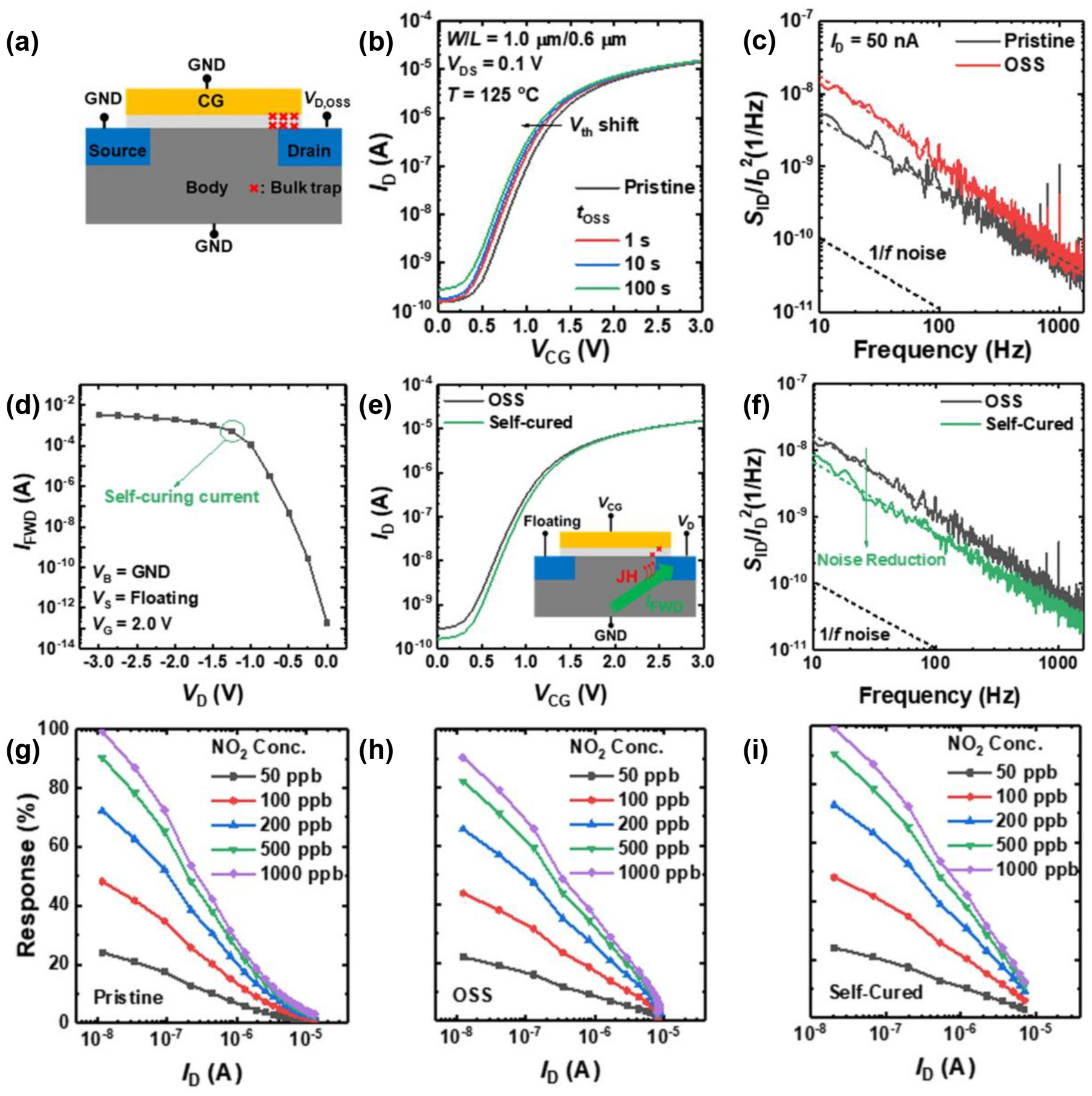
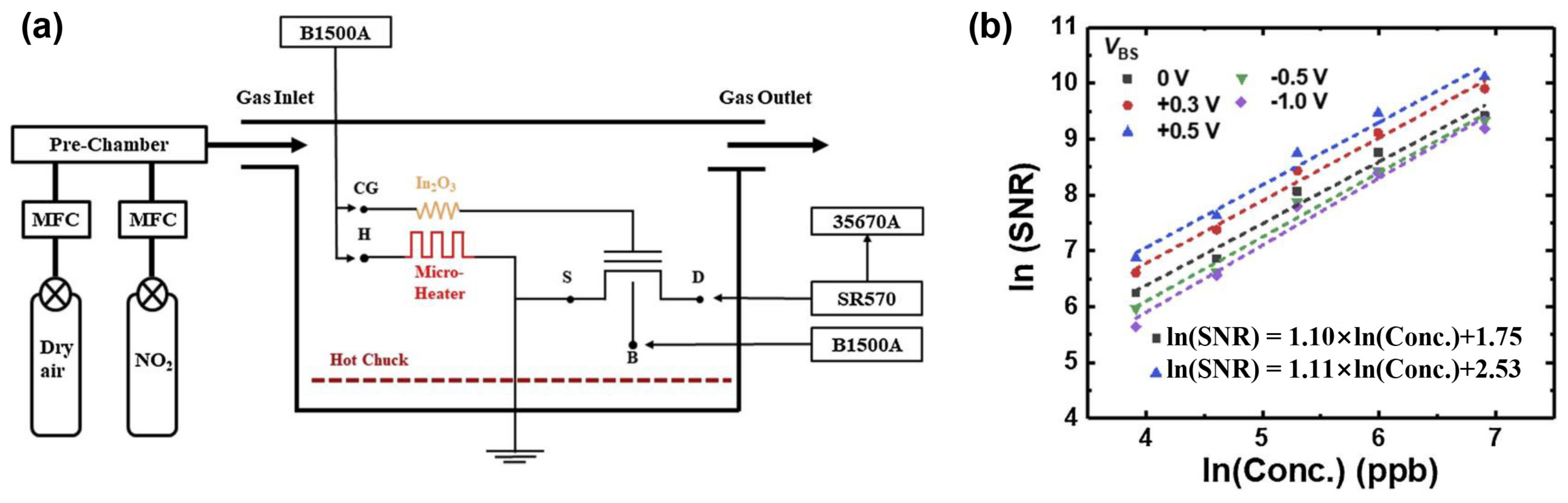
3.2. Signal–to–Noise Ratio

The signal–to–noise ratio (SNR) refers to the ratio of the intensity of the received useful signal to that of the interfering noise. In the context of FET gas sensors, the discussion of SNR typically revolves around the low–frequency noise characteristics which may impact the accuracy and stability of the sensor. Therefore, the performance of the FET gas sensors can be enhanced by understanding and controlling the low–frequency noise characteristics.
In 2020, Wonjun Shin et al. investigated the effects of radio frequency sputtering power on the deposition rate and resistivity of the formed In2O3 thin films. The resistive sensor and MOSFET are adopted as transducers to detect H2S, aiming at exploring the influence on signal–to–noise ratio (SNR). The highest SNR observed in the In2O3 thin film–based resistive sensor occurred at the sputtering power that yielded the lowest resistivity, despite the device’s response not being maximal under these conditions. However, the deposition rate and resistivity, affected by the sputtering power, did not impact the low–frequency noise characteristics of the In2O3 MOSFET, which is determined by the channel of the MOSFET. Accordingly, the SNR of the MOSFET based on radio frequency sputtered.
In2O3 thin films outperformed that of a resistive–type device, as shown in Figure 6 [47]. In the same year, their group prepared 12nm–thick In2O3 thin films through RF radio frequency magnetron sputtering (5 mTorr, Ar:O2 ratio of 10:1) as H2S–sensitive material. Both the resistive sensor and MOSFET were employed to further study the low–frequency noise characteristics, mainly focusing on differentiating between intrinsic noise and additional noise caused by gas reactions. Similar to the previous work, the noise characteristics of resistive gas sensors were dominated by the polycrystalline sensing layer and influenced by the deposition conditions of the sensing material, whereas the intrinsic noise of the In2O3 MOSFET depended on the channel, and was thus not affected by the sensing material. The intensity of low–frequency noise in the sub–threshold region of the MOSFET based on RF–sputtered In2O3 thin films is approximately ten times lower than that of the resistive sensor. Furthermore, additional noise, generated from gas reactions, was measured through In2O3 thin films prepared with different Ar to O2 ratios. The thin films formed in atmospheres with higher O2 ratios exhibited stronger reactivity towards H2S. The gas–to–air noise ratio (GANR) values for resistive sensors reacting with H2S prepared in Ar and Ar/O2 mixed atmospheres were 1.9–2.3 and 3.8–4.1, respectively, indicating a significant increase in additional noise owing to gas reactions. In contrast, the corresponding GANR values for MOSFETs were both approximately 1, arguing that almost no additional noise increased. In summary, the MOSFET based on RF–sputtered In2O3 thin films demonstrated lower intrinsic noise and even no additional noise than corresponding resistive gas sensors, as shown in Figure 7 [48].
In the following year, their group fabricated 12 nm–thick In2O3 thin films by RF radio frequency magnetron sputtering (50 W, 5 mTorr) again as NO2–sensitive materials, with MOSFET as the transducer, studying the effect of bulk–source junction bias voltage on signal–to–noise ratio (SNR). Carrier number fluctuations dominated the 1/f noise of the FET device in all operational regions and the 1/f noise decreased by a factor of about 10 when an appropriate VBS = 0.5 V was applied [49]. Meanwhile, the SNR doubled, implying that the limit of detection of NO2 was reduced by half, from 0.55 ppb to 0.27 ppb, as illustrated in Figure 8. The research conducted by the group to enhance the signal–to–noise ratio evolved from material deposition to transducer comparison, ultimately culminating in the optimization of the transducer’s operating conditions.

3.3. Response and Recovery

Response and recovery times are significant indicators for gas sensors and there is a high demand for fast response and recovery in various scenarios such as toxic, hazardous, and explosive prevention. In 2019, Seongbin Hong et al. applied Pt–modified In2O3 to MOSFET utilizing inkjet printing technology. The optimal 5% Pt doping concentration and the best sensing temperature of 200 °C for detecting CO were determined. The response, recovery time, and responsivity of the Pt–In2O were significantly enhanced. Furthermore, the response time can be further reduced by applying Vpre to the control gate, albeit at the expense of a certain degree of responsivity. The recovery time can be shortened to approximately 10 s when Vpre was fixed at −2 V, as shown in Figure 9 [46].
In 2022, Li et al. fabricated an acetone gas sensor based on Nd–doped In2O3 (InNdO) FET and the channel was composed of 1D InNdO nanofibers with a network structure assumed by electrospinning. The optimal doping ratio of Nd was determined to be 3%, considering the specific surface area of synthetic nanofibers, switching the ratio and carrier concentration of the InNdO TFT. The sensor exhibited outstanding electrical performance, characterized by a high mobility of 5.5 cm2 V−1 s−1 and an on/off current ratio of 107. In addition, the 3% InNdO TFT exhibited a high response of 88 to 4 ppm acetone at room temperature, with a response time of 31 s and a recovery time of 53 s, as illustrated in Figure 10 [61].
In 2023, Gyuho Yeom et al. prepared 12 nm In2O3 thin films by RF magnetron sputtering (5 mTorr, 50 W, Ar:O2 ratio of 15:1) to detect NO2. A TFT with a floating gate as the transducer was utilized to detect NO2 with rapid response and recovery at 75 °C. The swift response was attributed to the erase bias (Vers) method, which transferred electrons stored on the floating gate to the sensitive film, enabling sufficient electrons to react quickly with NO2, and enhancing the responsivity of the sensor simultaneously. Moreover, the fast recovery was facilitated by the pulse bias method. Electrons transferred back to the gate when applying a negative bias to the control gate, leading to rapid desorption of NO2 and NO2 could desorb quickly even at a low temperature of 75 °C, as shown in Figure 11. Obviously, the greater the pulse bias, the faster the desorption rate of NO2 [63]. Regarding the realization of fast response and recovery times in gas sensors, more attention is focused on material modification in addition to traditional external excitation methods such as lighting and heating. Furthermore, FET devices can also be optimized by adjusting operational conditions.

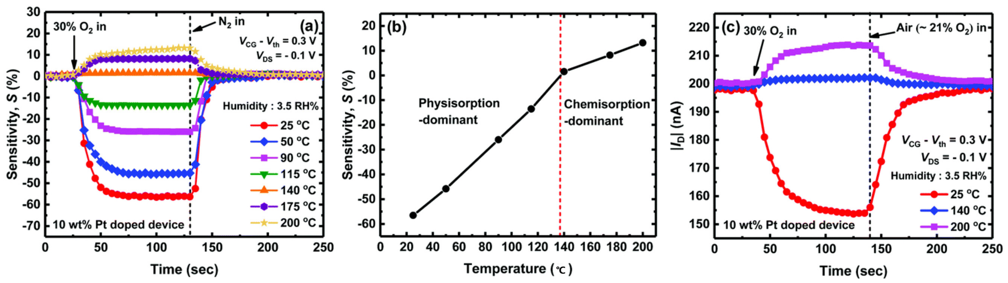
3.4. Low–Temperature Detection Capability

Metal oxide gas sensors typically require operation at high temperatures, which is not conducive to energy conservation and environmental protection, especially in long–term applications such as gas monitoring systems. Long–term high–temperature operation can even pose extra risks in some cases. Conversely, reducing the operating temperature can solve these issues and expand the range of applications. Therefore, achieving low–temperature detection capability for metal oxide gas sensors is one of the core pursuits in this field.
In 2012, porous indium oxide–based TFT sensors achieved acceptable ethanol selectivity at temperatures below 100 °C. In 2013, gold nanoparticle–modified Mg–In2O3 nanowire FET arrays realized the recognition of CO in mixed gas at room temperature [56,74]. In 2015, Wang et al. dissolved oily In2O3 nanoparticles in organic solvents and prepared the In2O3 TFT by spin–coating and annealing on silicon substrates. Significant changes were observed in electron mobility and current switching ratio by comparing the electrical characteristics of the TFT in air and nitrogen, indicating the sensitivity of the In2O3 TFT to O2 at room temperature [57]. In 2017, a TFT with a 1D nanowire mesh structure based on Sn–doped In2O3 as the conductive channel achieved the detection of 20 ppm H2S with a dynamic response time of several seconds at room temperature, which was assisted by laser [58]. In 2018, Seongbin Hong et al. prepared Pt–doped In2O3 MOSFET O2 sensors utilizing inkjet printing. Oxygen sensing at room temperature was achieved after optimizing the Pt doping concentration. The room–temperature oxygen–sensing behavior was due to physical adsorption, thus exhibiting excellent repeatability, as shown in Figure 12. Additionally, pulsed bias voltages that typically affect chemical adsorption had no effect on physical adsorption [45]. In 2020, an ethanol gas sensor based on Yb–doped In2O3 (InYbO) nanofiber TFT achieved a detection limit of 1 ppm for ethanol at temperatures below 80 °C. The 3% InNdO TFT managed a high response of 88 to 4 ppm acetone at room temperature, with a response time of 31 s and a recovery time of 53 s [59]. In 2022, the TFT gas sensor based on Yb–doped In2O3 (InYbO) nanofibers for detecting DMF also demonstrated rapid response and recovery to 89–2000 ppb DMF below 80 °C [60]. In the same year, a h–In2O3/SWNT FET gas sensor based on silicon and flexible substrate realized a detection limit of 1 ppm NO2 at room temperature [62]. In 2023, a NO2 gas sensor demonstrating rapid response and recovery capabilities was developed at 75 °C through the electron transfer mechanism between the gate and channel, attributed to the rapid desorption of NO2 resulting from electron motion under the influence of an electric field [63]. The advancements in gas sensing behavior at room temperature mainly stem from material modifications, including preparation methods and composites. Traditional external stimuli such as light exposure have been less explored in the field of FET gas sensors in recent years, while the ability to achieve this goal through gate voltage modulation of FET devices is gradually gaining momentum.

3.5. Selectivity

The selectivity of a gas sensor refers to its ability to identify specific gases and it depends on the working principles, materials, and design. The following are common methods to enhance the selectivity of gas sensors. First, the selection of sensitive materials is universal. Different gas sensing elements exhibit varying selectivity towards different gases and therefore choosing the appropriate sensing material can enhance the ability to recognize the target gas. Second, filtering techniques by adsorbents or membranes are beneficial for eliminating interfering gases. A selective barrier can be established around the sensor, allowing only the target gas to pass through, thereby enhancing selectivity. Third, changing the sensing temperature not only alters the sensing mode of physical or chemical adsorption on the sensor, but also modifies the mechanisms involved in chemical reactions. Hence, the selectivity can be controlled by the operating temperature. Fourth, the data processing algorithm meets the requirements of electronic nose. The accuracy and selectivity can be improved by utilizing data processing algorithms to analyze the fluctuating signals collected by the sensor. Fifth, gas sensor arrays and differential signal processing can be employed to eliminate interference and enhance selectivity. Sixth, gate voltage can provide additional modulation of internal charge carriers and enable selective design arrangements for FET gas sensors.
In 2012, M. Seetha and D. Mangalaraj prepared an ethanol TFT sensor based on porous indium oxide thin films using indium chloride solution as a precursor through a drop–coating method. The sensor demonstrated a significantly higher response to ethanol compared to ammonia and acetone, exhibiting minimal response variation within the relative humidity range of 40–60% [56]. In 2013, Zou et al. proposed an FET gas sensor with specific selectivity for different gases based on a quasi–one–dimensional Mg–doped indium oxide nanostructure modified with different metal nanoparticles. The traditional In2O3 FET gas sensor reacts to both oxidizing and reducing gases, but the reported E–mode of the prepared FET device is unable to respond to oxidizing gases due to the high threshold voltage, as shown in Figure 13a. Therefore, one–to–one selectivity enhancement for reducing gases can be achieved by intentionally modifying the channel–sensitive materials with special metal nanoparticles. The Mg–In2O3 nanowire FET modified with gold nanoparticles exhibited a response of over three orders of magnitude to 100 ppm CO exposed in a mixed gas under E–mode, with a response time of 4 s and a detection limit of 500 ppb. Similarly, silver nanoparticles and platinum nanoparticles–modified Mg–In2O3 nanowire FETs showed enhanced selectivity towards ethanol and hydrogen under E–mode, as shown in Figure 13b,c [74]. In 2020, Chen et al. prepared a TFT gas sensor towards N, N–Dimethylformamide (DMF) utilizing the electrospinning method, with the channel material composed of a network structure of one–dimensional nanofibers. The annealed nanofibers possessed a high specific surface area, and the FET devices based on nanofibers exhibited excellent electrical performance. Hence, the sensor displayed significant response to 89–2000 ppb DMF with response and recovery times of 36 and 67 s, respectively. Specifically, exceptional selectivity towards DMF was proved among the testing of five organic gases containing DMF, toluene, xylene, ethanol, and acetone, as illustrated in Figure 13 (right graph side) [60]. FET gas sensors can achieve enhanced selectivity not only through material considerations but also through a synergistic combination of mechanism–based and material–based designs, contrasting with the extensively researched resistive sensors.

4. Performance Optimization of In2O3 FET Gas Sensors

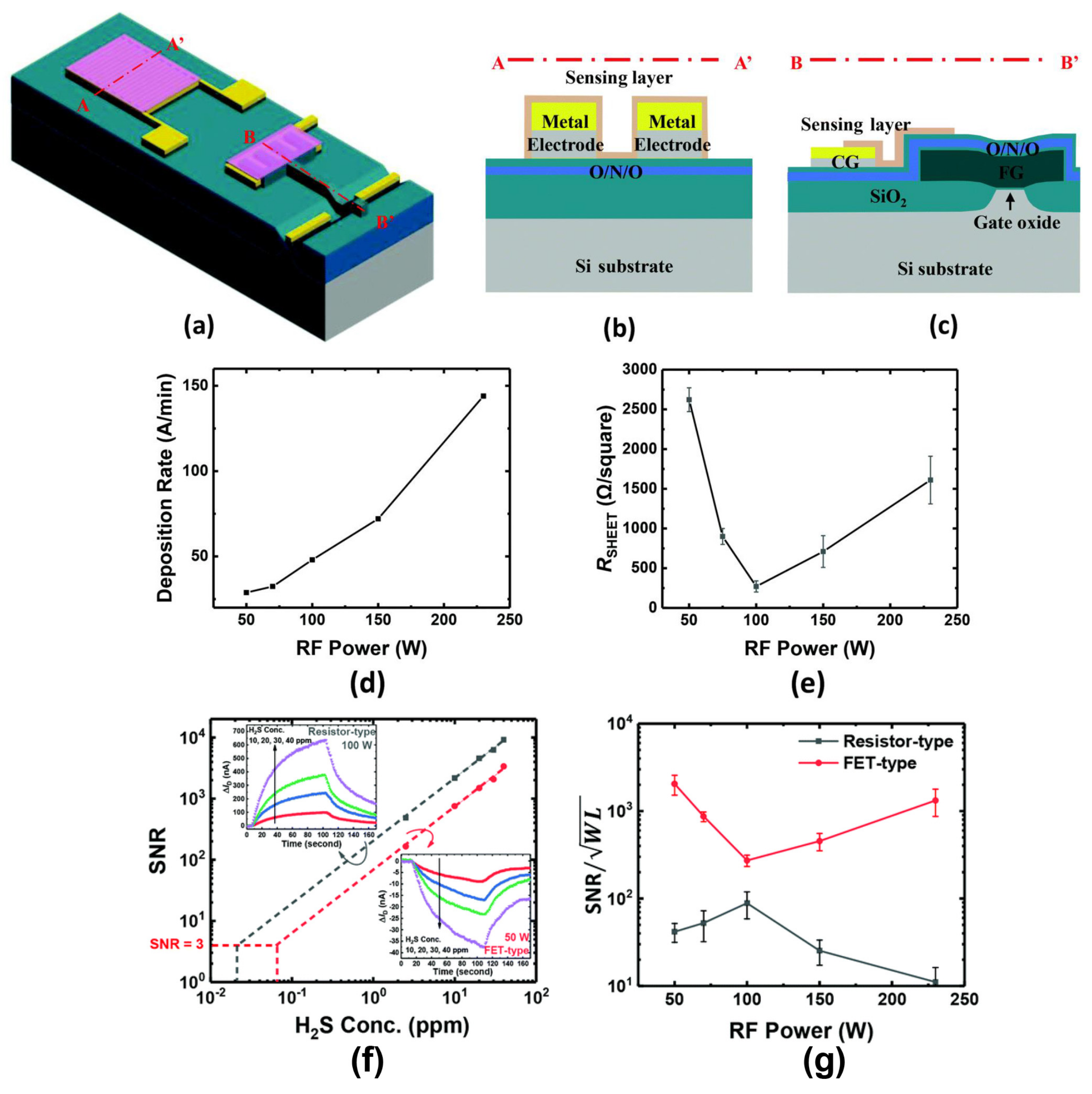
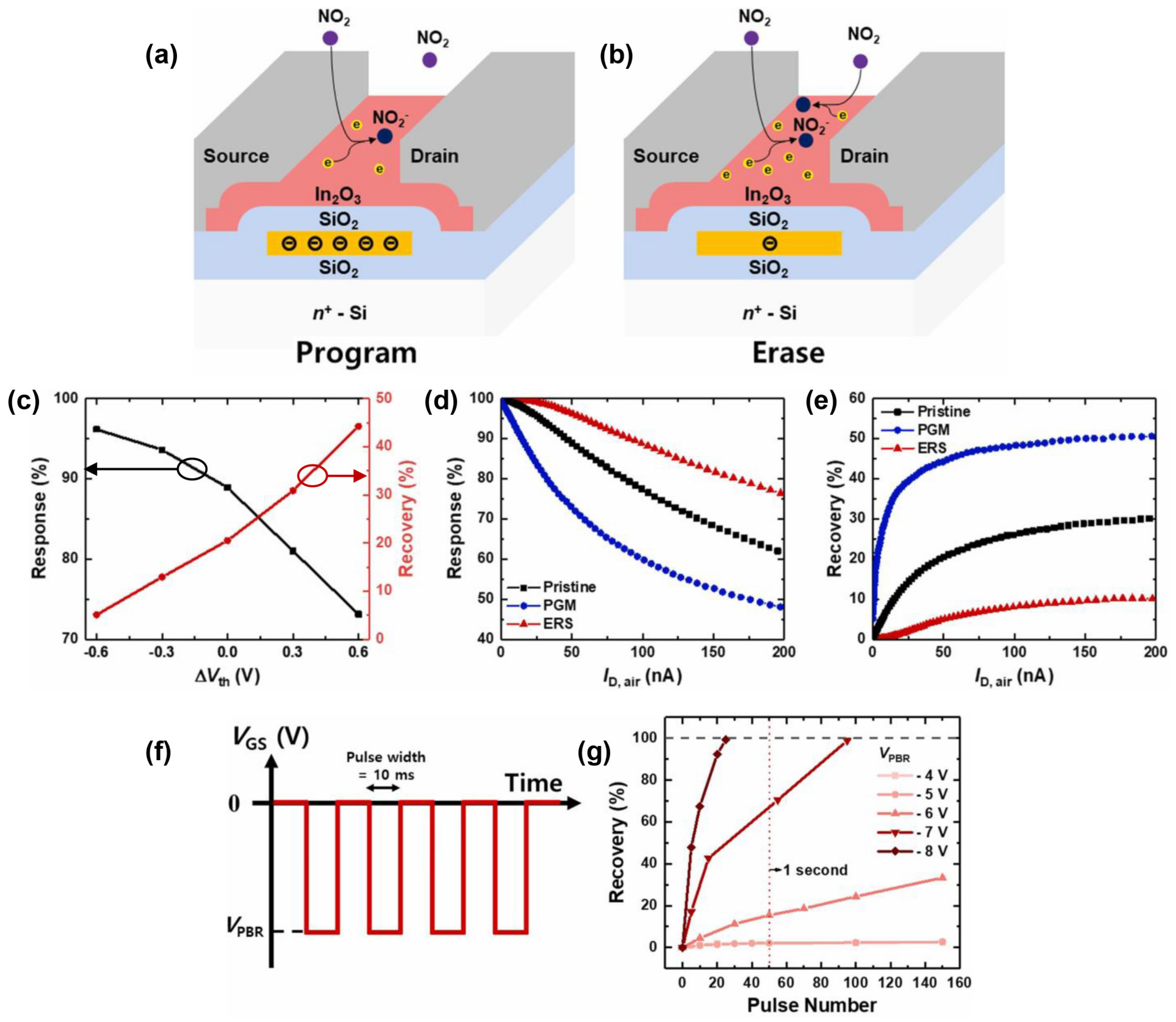
4.1. Optimization of FET Struture

The application of In2O3–based gas sensors is well established, but most current research predominantly concentrates on the modification of sensitive materials. The structure of gas sensors based on In2O3 FETs, including gate materials, source–drain contacts, built–in heaters, and electric fields, significantly influences the performance of gas sensing. It has been mentioned earlier that polycrystalline silicon gates can enhance the output saturation current, transconductance, and response to H2S compared to conventional metal gates in MOSFETs [55]. In 2017, Zeng et al. introduced heavily doped ATO (antimony–doped tin oxide) as drain and source electrodes in contact with metal oxide nanowires, demonstrating more stable and lower contact resistance, in comparison with the situations based on traditional Ti contacts, as shown in Figure 14e. Moreover, the stability and low contact resistance of ATO persisted for at least 1960 h in open–air environments at 200 °C while sustaining sensitivity and response to NO2 without degradation. The optimization in long–term stability has been realized by replacing the source–drain conventional metal materials with metal oxides of the FET gas sensor, as illustrated in Figure 14f–h [75]. Additionally, the MOSFETs featuring a floating gate structure demonstrate the potential applications of FET gas sensors [45,46,47,48,49,50,51,52,53,54,55]. Furthermore, even parameters such as the aspect ratio and width of the cross–finger electrodes in FET channels have an impact on device performance and gas sensing properties [54].
The optimization of the channel for TFT gas sensors is crucial, since it serves as both the carrier transport layer and the target gas–sensitive layer. Therefore, the channel not only determines the electrical performance of FETs but also fundamentally influences the reactions with target gases. One–dimensional (1D) nanowires offer advantages as the channels of FET gas sensors for several reasons. First, the high surface area–to–volume ratio of 1D nanowires can increase the interaction sites with gas molecules, leading to improved sensitivity in gas sensing applications. Second, charge carrier mobility can be improved due to their small size and high crystallinity and 1D nanowires can facilitate efficient charge carrier transport, resulting in enhanced electrical conductivity and device performance. Third, properties such as conductivity and bandgap are tunable and can be tailored by adjusting size, composition, and morphology, enabling optimization for specific application requirements. Fourth, 1D nanowires can be integrated into scalable fabrication processes compatible with existing semiconductor technologies, enabling their incorporation into complex electronic devices and systems. Overall, 1D nanowires present promising opportunities for realizing high–performance FET channels with enhanced functionality and versatility.
In 2013, Zou et al. proposed a “one–key to one–lock” hybrid sensor configuration based on 1D Mg–In2O3 nanowires, for selective detection of specific reducing gases in complex environmental backgrounds. Traditional In2O3 FETs in D–mode respond to both oxidizing and reducing gases. However, the threshold voltage of the FET can be increased to form an E–mode by adjusting the Mg doping concentration, in which the device does not respond to oxidizing gases. Further selective detection of reducing gases is achieved by specific modifications with different metal nanoparticles. Specifically, the nanowires modified with Au, Ag, and Pt nanoparticles were sensitive to CO, ethanol, and H2, correspondingly [74].
One–dimensional metal oxide nanowires serve as excellent functional units for integrated and transparent electronic devices. However, the synthesis methods are typically uncontrollable and involve random distribution, which pose challenges for mass production. In 2019, Tae–Sik Kim et al. introduced a large–scale direct printing approach for versatile nanoscale metal oxide nanowire electronic devices. This approach offers several advantages such as highly aligned, digitally controlled, and arbitrarily long metal oxide wire (MOW) arrays, as shown in Figure 15. In addition, the applications in gas sensing were verified. The method involves high–pressure direct printing of sacrificial polymer and precursor solutions onto a silicon substrate, followed by sintering to form the MOW array. The top contact electrode is fabricated using the conventional metal thermal evaporation process. Large–scale manufacturing and precise control of the MOW process can be achieved through this direct printing approach, leading to improved stability and reliability of FET gas sensors [76]. Large–area controllable preparation of 1D nanowires is one of the future development directions.

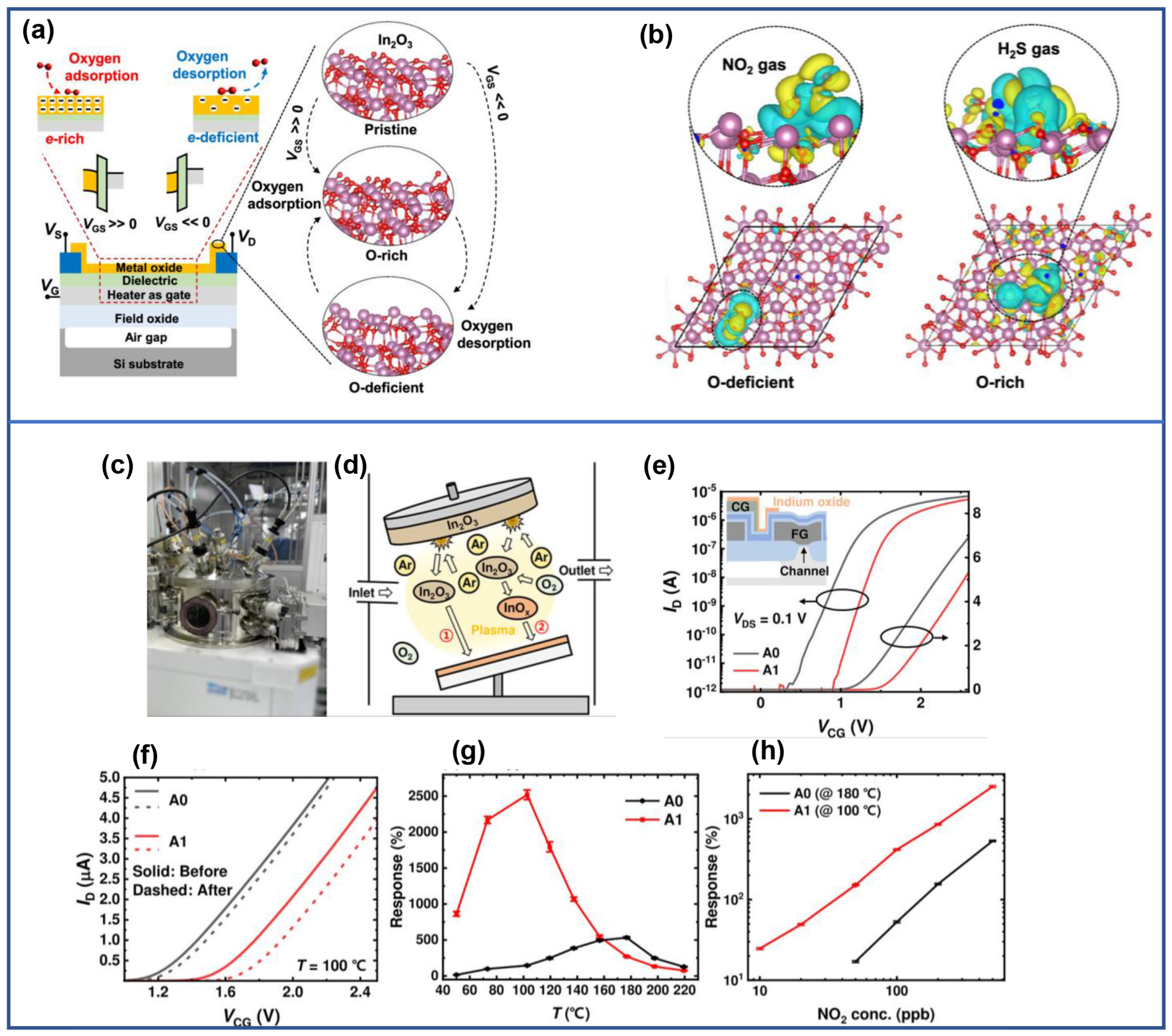
4.2. Optimization of Operating Conditions

Optimizing the operating conditions of sensors to enhance gas sensing performance is a common approach for FETs. The design of FETs aims to amplify the current under the influence of the gate electrical field, which effectively amplifies the gas sensing response. Firstly, the positive or negative bias of the control gate voltage, Vpre, applied before gas measurement, can selectively enhance the response to oxidative gases such as NO2 or reductive gases such as H2S. Additionally, selecting the appropriate polarity of gate voltage bias after gas testing can accelerate the desorption and reduce recovery time. Secondly, integrating a microheater into FETs facilitates the operation at optimal temperature to achieve the best response, sensitivity, and response or recovery time. Thirdly, biasing through pulse voltage instead of DC voltage can generally improve the electrical performance of FETs, thereby enhancing gas sensing performance. Fourthly, appropriate biasing of the body–source junction can not only increase the signal–to–noise ratio of the MOSFET gas sensors, but also partially repair repeatability and stability caused by off–state stress damage. Finally, external stimuli such as light exposure can greatly enhance gas sensing performance.

4.3. Algorithm

In 2021, Dongseok Kwon et al. utilized the same sensor to predict the concentrations of NO2 and H2S by training algorithms involving Recurrent Neural Networks (RNNs) and Fully Connected Neural Networks (FCNNs), with the transient responses reflecting the concentrations of target gases and operating temperatures. Even with fewer input neurons, RNN with an error rate of 1.94% outperformed FCNN with an error rate of 3.02% following the training of RNN and FCNN in the PyTorch framework [77]. Subsequent to this work, their group fabricated a MOSFET based on In2O3 thin film, and the responses towards NO2 and H2S under different operating temperatures, gate voltages, and gas concentrations were utilized as the training set. A low prediction error rate of approximately 3% for gas concentration was achieved through the employment of the Spiking Neural Networks (SNN) algorithm. Furthermore, the operational time of the SNN was around 5 s, making it suitable for rapid detection [78]. Both endeavors concerning gas concentration prediction, as shown in Figure 16, were based on the dynamic transient response of FET gas sensors, akin to the parameter extraction of resistive sensors.
Extraction of multiple parameters from transfer and output characteristics of FET gas sensors offers advantages in predicting gas types and concentrations through algorithms. Unlike resistive gas sensors relying on transient dynamic response parameters such as response values and response times, FET gas sensors offer a wider range of extractable parameters from the transient transfer and output curves such as saturation output current, switching ratio, threshold voltage, carrier concentration and mobility, sub–threshold swing, etc. Variations in gate bias lead to changes in multiple measurement parameters, and these parameters can provide independent or partially independent outputs, resulting in two–dimensional and three–dimensional response distributions. Predictions based on three–dimensional distributions generally yield more accurate gas concentration estimates compared to those based on two–dimensional distributions [79,80].

5. Challenges and Future Perspectives

The high carrier concentration and mobility of indium oxide are key reasons for its high gas sensing sensitivity. Table 1 lists several types of In2O3 transistors with high mobility. In2O3 FET gas sensors have garnered significant interest owing to the potential for high sensitivity, low power consumption, and compatibility with integrated circuit technology [59,62,76]. However, they also face challenges like any technology and offer future perspectives.
A principal challenge lies in achieving high selectivity for specific target gases while effectively minimizing interference from other environmental gases. Enhancing selectivity often requires the integration of additional sensing materials or advanced signal processing techniques [59,60,61]. Firstly, various preparation methods yield diverse material and gas sensing characteristics for materials primarily composed of In2O3. Incorporation of metallic nanoparticles, rare earth element doping, common metal oxide composites, and composites including carbon–based compounds, graphene, and MXene, etc. enhance the selectivity to some extent. Therefore, continued research in material engineering including exploring novel nanostructures, doping techniques, and surface functionalization methods is crucial for enhancing the selectivity of In2O3 FET gas sensors [46,50]. Secondly, external stimuli such as temperature and illumination can alter the sensing modes of gas reactions through physical or chemical adsorption. Consequently, selectivity can be controlled in specific scenarios by this method [45]. Thirdly, the utilization of gate voltage can provide additional modulation of charge carriers in the channel, thereby enhancing or suppressing the reactions towards oxidative or reductive gases [46,50,52]. Fourthly, the principal component analysis (PCA) implemented through algorithms on the test data of gas sensors is a mainstream method to effectively improve the selectivity of In2O3 FET. The multi–parameter extraction of FETs is beneficial for achieving the three–dimensional distribution of PCA and more accurately predicting gas types and concentrations [77,78,79,80].
Although the stable properties of In2O3 have been verified, the long–term stability of the composites needs to be investigated. These FET gas sensors may experience performance degradation over time due to environmental factors such as humidity, temperature variations, and exposure to target gases. Ensuring long–term stability and reliability is crucial for practical applications [62]. Another unstable factor is the contact between the source/drain electrodes and the channel material, In2O3. Ti or Cr is commonly adopted as a direct contact metal with In2O3 due to the influence of contact resistance. However, these two metals can be oxidized over a period, leading to instability and unreliability of FETs. Studies on doped metal oxides replacing the conventional Ti/Cr demonstrated more stable source/drain contact. Therefore, further exploration to investigate the stable contact is necessary [75].
Despite advancements in miniaturizing In2O3 FET gas sensors, additional efforts are required to integrate them into compact and portable devices for real–world applications. This requires addressing challenges related to fabrication techniques, signal processing circuitry, and power management. Generally, MOSFETs are smaller than TFTs, making them more conducive to integration. TFTs exhibit larger responses and higher signal–to–noise ratios, and smaller limits of gas detection. The specific type of sensor is determined by comprehensively considering the requirements in practical applications [53,76].
Enhancing both response and recovery times is crucial for applications that demand rapid detection and monitoring of gas concentrations. The rate and amount of transferred electrons, which influence the response and recovery times, plays a critical role in the oxidation or reduction reactions frequently occurring in gas sensors. Optimization of response and recovery times can be achieved through material engineering, such as doping, modification, composites, external stimuli, and internal electric fields via gate voltage [46,61,63].
In2O3 FET gas sensors regularly exhibit temperature–dependent behavior, which significantly impacts their performance and reliability, especially in fluctuating or extreme temperature environments. Developing strategies to mitigate temperature effects or implementing temperature compensation techniques is essential. The prolonged operation at high temperatures adversely affects the stability, reliability, and lifespan of the device. Therefore, achieving the target gas sensing at low temperatures or even at room temperature becomes particularly crucial. Advances in material engineering, combined with the internal electric fields generated by field–effect properties, present opportunities to achieve sensing at lower temperatures [56,74,85,86].
Overall, future perspectives of In2O3 FET gas sensors should emphasize material engineering, intelligent sensing systems, flexible and wearable devices, and interdisciplinary collaboration. Ongoing research in material engineering is crucial for enhancing the sensing performance of In2O3 FET gas sensors, which includes exploring novel nanostructures, doping techniques, and surface functionalization methods to improve sensitivity, selectivity, and stability. Integration with advanced signal processing algorithms, machine learning techniques, and wireless communication capabilities can enable the development of smart sensing systems capable of real–time monitoring, data analytics and autonomous decision–making. Expanding the application scope of In2O3 FET gas sensors to flexible and wearable devices has the potential to revolutionize healthcare, environmental monitoring, and personal safety applications. Research efforts should focus on developing flexible substrates, scalable fabrication processes, and biocompatible sensor interfaces. Collaborations among researchers in materials science, electrical engineering, chemistry, and other related fields are essential for driving innovation in In2O3 FET gas sensor technology. Interdisciplinary approaches can lead to breakthroughs in sensor design, fabrication, and integration with complementary technologies. With continued advancements, these sensors could play a pivotal role in addressing environmental challenges.

Author Contributions

Conceptualization, C.L. and Y.H.; writing—original draft preparation, C.L.; writing—review and editing, C.L., Z.C., J.H., S.Z., Y.Y., Y.D., H.L., C.H., Y.Z. and Y.H.; supervision, C.L., Z.C., J.H., S.Z., Y.Y., Y.D., H.L., C.H., C.G., Y.Z. and Y.H.; project administration, C.G., Y.Z. and Y.H. All authors have read and agreed to the published version of the manuscript.

Funding

This research was funded by the Natural Science Foundation of Chongqing (cstc2020jscx–dxwtBX0052, CSTB2022NSCQ–LZX0075), the Fundamental Research Funds for Central Universities of China (2021CDJXDJH006, 2022CDJJMRH–006 and 2023CDJXY–040), and the Key Laboratory of Gun Launch and Control Technology, NORINCO.

Conflicts of Interest

The authors declare no conflicts of interest.

References

  1. Nadargi, D.Y.; Umar, A.; Nadargi, J.D.; Lokare, S.A.; Akbar, S.; Mulla, I.S.; Suryavanshi, S.S.; Bhandari, N.L.; Chaskar, M.G. Gas sensors and factors influencing sensing mechanism with a special focus on MOS sensors. J. Mater. Sci. 2023, 58, 559–582. [Google Scholar] [CrossRef]
  2. Verma, A.; Gupta, R.; Verma, A.S.; Kumar, T. Review–Recent Advances and Challenges of Conducting Polymer–Metal Nanocomposites for the Detection of Industrial Waste Gases. ECS J. Solid State Sci. Technol. 2023, 12, 20. [Google Scholar] [CrossRef]
  3. Ryabtsev, S.V.; Shaposhnick, A.V.; Lukin, A.N.; Domashevskaya, E.P. Application of semiconductor gas sensors for medical diagnostics. Sens. Actuator B–Chem. 1999, 59, 26–29. [Google Scholar] [CrossRef]
  4. Joshi, N.; Pransu, G.; Conte, C.A. Critical review and recent advances of 2D materials–Based gas sensors for food spoilage detection. Crit. Rev. Food Sci. Nutr. 2023, 63, 10536–10559. [Google Scholar] [CrossRef] [PubMed]
  5. Preethichandra, D.M.G.; Gholami, M.D.; Izake, E.L.; O’Mullane, A.P.; Sonar, P. Conducting Polymer Based Ammonia and Hydrogen Sulfide Chemical Sensors and Their Suitability for Detecting Food Spoilage. Adv. Mater. Technol. 2023, 8, 34. [Google Scholar] [CrossRef]
  6. Balan, T.; Dumitru, C.; Dudnik, G.; Alessi, E.; Lesecq, S.; Correvon, M.; Passaniti, F.; Licciardello, A. Smart Multi–Sensor Platform for Analytics and Social Decision Support in Agriculture. Sensors 2020, 20, 29. [Google Scholar] [CrossRef]
  7. Man, G.; Stoeber, B.; Walus, K. An assessment of sensing technologies for the detection of clandestine methamphetamine drug laboratories. Forensic Sci. Int. 2009, 189, 1–13. [Google Scholar] [CrossRef]
  8. Sun, Z.G.; Huang, L.X.; Zhang, Y.; Wu, X.F.; Zhang, M.H.; Liang, J.H.; Bao, Y.W.; Xia, X.H.; Gu, H.S.; Homewood, K.; et al. Homojunction TiO2 thin film–based room–temperature working H2 sensors with non–noble metal electrodes. Sens. Actuator B–Chem. 2024, 398, 11. [Google Scholar] [CrossRef]
  9. Epping, R.; Koch, M. On–Site Detection of Volatile Organic Compounds (VOCs). Molecules 2023, 28, 19. [Google Scholar] [CrossRef]
  10. Majhi, S.M.; Mirzaei, A.; Kim, H.W.; Kim, S.S.; Kim, T.W. Recent advances in energy–saving chemiresistive gas sensors: A review. Nano Energy 2021, 79, 25. [Google Scholar] [CrossRef]
  11. Li, Z.J.; Li, H.; Wu, Z.L.; Wang, M.K.; Luo, J.T.; Torun, H.D.; Hu, P.A.; Yang, C.; Grundmann, M.; Liu, X.T.; et al. Advances in designs and mechanisms of semiconducting metal oxide nanostructures for high–precision gas sensors operated at room temperature. Mater. Horiz. 2019, 6, 470–506. [Google Scholar] [CrossRef]
  12. Moseley, P.T. Progress in the development of semiconducting metal oxide gas sensors: A review. Meas. Sci. Technol. 2017, 28, 15. [Google Scholar] [CrossRef]
  13. Chu, J.F.; Li, W.J.; Yang, X.; Wu, Y.; Wang, D.W.; Yang, A.J.; Yuan, H.; Wang, X.H.; Li, Y.J.; Rong, M.Z. Identification of gas mixtures via sensor array combining with neural networks. Sens. Actuator B–Chem. 2021, 329, 10. [Google Scholar] [CrossRef]
  14. Song, X.Y.; Liu, T.; Gu, K.K.; Luo, Z.B.; Zhang, M.Z. Highly selective and ultra–sensitive gas sensor based on Fe2O3/Ti3C2Tx MXene heterostructure for ppb–level n–butanol detection. J. Alloy Compd. 2024, 976, 10. [Google Scholar] [CrossRef]
  15. Lee, J.; Gam, D.; Nam, K.E.; Cho, S.J.; Kim, H. Feasibility study of a resistive–type sodium aerosol detector with ZnO nanowires for sodium–cooled fast reactors. Nucl. Eng. Technol. 2023, 55, 2373–2379. [Google Scholar] [CrossRef]
  16. Potyrailo, R.A. Multivariable Sensors for Ubiquitous Monitoring of Gases in the Era of Internet of Things and Industrial Internet. Chem. Rev. 2016, 116, 14918. [Google Scholar] [CrossRef]
  17. Singh, E.; Meyyappan, M.; Nalwa, H.S. Flexible Graphene–Based Wearable Gas and Chemical Sensors. ACS Appl. Mater. Interfaces 2017, 9, 34544–34586. [Google Scholar] [CrossRef]
  18. Kumar, R.; Liu, X.H.; Zhang, J.; Kumar, M. Room–Temperature Gas Sensors Under Photoactivation: From Metal Oxides to 2D Materials. Nano–Micro Lett. 2020, 12, 37. [Google Scholar] [CrossRef]
  19. Lu, H.; Seabaugh, A. Tunnel Field–Effect Transistors: State–of–the–Art. IEEE J. Electron Devices Soc. 2014, 2, 44–49. [Google Scholar] [CrossRef]
  20. Qiu, C.G.; Zhang, Z.Y.; Xiao, M.M.; Yang, Y.J.; Zhong, D.L.; Peng, L.M. Scaling carbon nanotube complementary transistors to 5–nm gate lengths. Science 2017, 355, 271–276. [Google Scholar] [CrossRef]
  21. Xu, K.K. Silicon MOS Optoelectronic Micro–Nano Structure Based on Reverse–Biased PN Junction. Phys. Status Solidi A–Appl. Mat. 2019, 216, 9. [Google Scholar] [CrossRef]
  22. Paghi, A.; Mariani, S.; Barillaro, G. 1D and 2D Field Effect Transistors in Gas Sensing: A Comprehensive Review. Small 2023, 19, 61. [Google Scholar] [CrossRef] [PubMed]
  23. Hong, S.; Wu, M.; Hong, Y.; Jeong, Y.; Jung, G.; Shin, W.; Park, J.; Kim, D.; Jang, D.; Lee, J.H. FET–type gas sensors: A review. Sens. Actuator B–Chem. 2021, 330, 24. [Google Scholar] [CrossRef]
  24. Zeng, S.M.; Zhang, Y.; Zhang, Y.; Li, Y.N.; Tang, C.G.; Li, K.; Sun, J.Y.; Deng, T. A novel room temperature SO2 gas sensor based on TiO2/rGO buried–gate FET. Microelectron. Eng. 2022, 263, 7. [Google Scholar] [CrossRef]
  25. Shaji, M.; Saji, K.J.; Jayaraj, M.K. Low temperature operated ZTO thin film transistor based gas sensor for selective detection of H2S. Mater. Sci. Semicond. Process 2022, 150, 7. [Google Scholar] [CrossRef]
  26. Liao, F.; Chen, C.; Subramanian, V. Organic TFTs as gas sensors for electronic nose applications. Sens. Actuator B Chem. 2005, 107, 849–855. [Google Scholar] [CrossRef]
  27. Han, J.K.; Kang, M.; Jeong, J.; Cho, I.; Yu, J.M.; Yoon, K.J.; Park, I.; Choi, Y.K. Artificial Olfactory Neuron for an In–Sensor Neuromorphic Nose. Adv. Sci. 2022, 9, 11. [Google Scholar] [CrossRef]
  28. Yoshizumi, T.; Goda, T.; Yatabe, R.; Oki, A.; Matsumoto, A.; Oka, H.; Washio, T.; Toko, K.; Miyahara, Y. Field–effect transistor array modified by a stationary phase to generate informative signal patterns for machine learning–assisted recognition of gas–phase chemicals. Mol. Syst. Des. Eng. 2019, 4, 386–389. [Google Scholar] [CrossRef]
  29. Chen, Y.; Huang, W.; Sangwan, V.K.; Wang, B.H.; Zeng, L.; Wang, G.; Huang, Y.; Lu, Z.Y.; Bedzyk, M.J.; Hersam, M.C.; et al. Polymer Doping Enables a Two–Dimensional Electron Gas for High–Performance Homojunction Oxide Thin–Film Transistors. Adv. Mater. 2019, 31, 8. [Google Scholar] [CrossRef]
  30. Liu, Y.Y.; Meng, F.Y.; Shi, J.H.; Huang, W.; Liu, W.Z.; Liu, Z.X. High mobility Ti, Zr and Ga–codoping In2O3 transparent conductive oxide films prepared at low temperatures. J. Mater. Sci.–Mater. Electron. 2021, 32, 3201–3210. [Google Scholar] [CrossRef]
  31. Huang, W.; Yu, X.G.; Zeng, L.; Wang, B.H.; Takai, A.; Di Carlo, G.; Bedzyk, M.J.; Marks, T.J.; Facchetti, A. Ultraviolet Light–Densified Oxide–Organic Self–Assembled Dielectrics: Processing Thin–Film Transistors at Room Temperature. ACS Appl. Mater. Interfaces 2021, 13, 3445–3453. [Google Scholar] [CrossRef]
  32. Zhang, X.N.; Wang, B.H.; Huang, W.; Chen, Y.; Wang, G.; Zeng, L.; Zhu, W.G.; Bedzyk, M.J.; Zhang, W.F.; Medvedeva, J.E.; et al. Synergistic Boron Doping of Semiconductor and Dielectric Layers for High–Performance Metal Oxide Transistors: Interplay of Experiment and Theory. J. Am. Chem. Soc. 2018, 140, 12501–12510. [Google Scholar] [CrossRef]
  33. Pham, A.T.; Luu, O.A.M.; Nguyen, A.D.; Chu, M.H. Porous In2O3 nanorods fabricated by hydrothermal method for an effective CO gas sensor. Mater. Res. Bull. 2021, 137, 9. [Google Scholar]
  34. Son, D.N.; Hung, C.M.; Le, D.T.T.; Xuan, C.T.; Van Duy, N.; Dich, N.Q.; Nguyen, H.; Van Hieu, N.; Hoa, N.D. A novel design and fabrication of self–heated In2O3 nanowire gas sensor on for ethanol detection. Sens. Actuator A–Phys. 2022, 345, 11. [Google Scholar] [CrossRef]
  35. Cheng, P.F.; Wang, Y.L.; Wang, C.; Ma, J.; Xu, L.P.; Lv, C.; Sun, Y.F. Investigation of doping effects of different noble metals for ethanol gas sensors based on mesoporous In2O3. Nanotechnology 2021, 32, 15. [Google Scholar] [CrossRef] [PubMed]
  36. Luo, Y.B.; An, B.X.; Bai, J.L.; Wang, Y.R.; Cheng, X.; Wang, Q.; Li, J.P.; Yang, Y.F.; Wu, Z.K.; Xie, E.Q. Ultrahigh–response hydrogen sensor based on PdO/NiO co–doped In2O3nanotubes. J. Colloid Interface Sci. 2021, 599, 533–542. [Google Scholar] [CrossRef] [PubMed]
  37. Liu, Y.N.; Li, S.; Xiao, S.; Du, K. Down to ppb level NO2 detection by vertically MoS2 nanoflakes grown on In2O3 microtubes at room temperature. Colloid Surf. A–Physicochem. Eng. Asp. 2022, 648, 12. [Google Scholar] [CrossRef]
  38. Liu, M.; Song, P.; Yang, Z.X.; Wang, Q. MXene/In2O3nanocomposites for formaldehyde detection at low temperature. Inorg. Chem. Commun. 2023, 148, 8. [Google Scholar] [CrossRef]
  39. Du, N.; Zhang, H.; Chen, B.D.; Ma, X.Y.; Liu, Z.H.; Wu, J.B.; Yang, D.R. Porous indium oxide nanotubes: Layer–by–layer assembly on carbon–nanotube templates and application for room–temperature NH3 gas sensors. Adv. Mater. 2007, 19, 1641–1645. [Google Scholar] [CrossRef]
  40. Yi, S.; Tian, S.Q.; Zeng, D.W.; Xu, K.; Zhang, S.P.; Xie, C.S. An In2O3 nanowire–like network fabricated on coplanar sensor surface by sacrificial CNTs for enhanced gas sensing performance. Sens. Actuator B–Chem. 2013, 185, 345–353. [Google Scholar] [CrossRef]
  41. Hong, S.Z.; Huang, Q.Y.; Wu, T.M. Facile Synthesis of Polyaniline/Carbon–Coated Hollow Indium Oxide Nanofiber Composite with Highly Sensitive Ammonia Gas Sensor at the Room Temperature. Sensors 2022, 22, 13. [Google Scholar] [CrossRef] [PubMed]
  42. Fatema, K.N.; Sagadevan, S.; Liu, Y.; Cho, K.Y.; Jung, C.H.; Oh, W.C. New design of mesoporous SiO2 combined In2O3–graphene semiconductor nanocomposite for highly effective and selective gas detection. J. Mater. Sci. 2020, 55, 13085–13101. [Google Scholar] [CrossRef]
  43. Liu, X.J.; Jiang, L.; Jiang, X.M.; Tian, X.Y.; Huang, Y.; Hou, P.Y.; Zhang, S.W.; Xu, X.J. Design of superior ethanol gas sensor based on indium oxide/molybdenum disulfide nanocomposite via hydrothermal route. Appl. Surf. Sci. 2018, 447, 49–56. [Google Scholar] [CrossRef]
  44. Mansha, M.; Qurashi, A.; Ullah, N.; Bakare, F.O.; Khan, I.; Yamani, Z.H. Synthesis of In2O3/graphene heterostructure and their hydrogen gas sensing properties. Ceram. Int. 2016, 42, 11490–11495. [Google Scholar] [CrossRef]
  45. Hong, S.; Shin, J.; Hong, Y.; Wu, M.; Jang, D.; Jeong, Y.; Jung, G.; Bae, J.H.; Jang, H.W.; Lee, J.H. Observation of physisorption in a high–performance FET–type oxygen gas sensor operating at room temperature. Nanoscale 2018, 10, 18019–18027. [Google Scholar] [CrossRef]
  46. Hong, S.; Hong, Y.; Jeong, Y.; Jung, G.; Shin, W.; Park, J.; Lee, J.K.; Jang, D.; Bae, J.H.; Le, J.H. Improved CO gas detection of Si MOSFET gas sensor with catalytic Pt decoration and pre–bias effect. Sens. Actuator B–Chem. 2019, 300, 8. [Google Scholar] [CrossRef]
  47. Shin, W.; Jung, G.; Hong, S.; Jeong, Y.; Park, J.; Kim, D.; Jang, D.; Kwon, D.; Bae, J.H.; Park, B.G.; et al. Proposition of deposition and bias conditions for optimal signal–to–noise–ratio in resistor– and FET–type gas sensors. Nanoscale 2020, 12, 19768–19775. [Google Scholar] [CrossRef]
  48. Shin, W.; Jung, G.; Hong, S.; Jeong, Y.; Park, J.; Jang, D.; Park, B.G.; Lee, J.H. Low frequency noise characteristics of resistor– and Si MOSFET–type gas sensors fabricated on the same Si wafer with In2O3 sensing layer. Sens. Actuator B–Chem. 2020, 318, 11. [Google Scholar] [CrossRef]
  49. Shin, W.; Hong, S.; Jung, G.; Jeong, Y.; Park, J.; Kim, D.; Jang, D.; Park, B.G.; Lee, J.H. Improved signal–to–noise–ratio of FET–type gas sensors using body bias control and embedded micro–heater. Sens. Actuator B–Chem. 2021, 329, 9. [Google Scholar] [CrossRef]
  50. Jung, G.; Hong, S.; Jeong, Y.; Shin, W.; Park, J.; Kim, D.; Bae, J.H.; Park, B.G.; Lee, J.H. Response Comparison of Resistor– and Si FET–Type Gas Sensors on the Same Substrate. IEEE Trans. Electron Devices 2021, 68, 3552–3557. [Google Scholar] [CrossRef]
  51. Shin, W.; Jeong, Y.; Kim, M.; Lee, J.; Koo, R.H.; Hong, S.; Jung, G.; Kim, J.J.; Lee, J.H. Recovery of off–state stress–induced damage in FET–type gas sensor using self–curing method. Discov. Nano. 2023, 18, 10. [Google Scholar] [CrossRef] [PubMed]
  52. Jung, G.; Ju, S.; Choi, K.; Kim, J.; Hong, S.; Park, J.; Shin, W.; Jeong, Y.; Han, S.; Choi, W.Y.; et al. Reconfigurable Manipulation of Oxygen Content on Metal Oxide Surfaces and Applications to Gas Sensing. ACS Nano 2023, 17, 17790–17798. [Google Scholar] [CrossRef] [PubMed]
  53. Jung, G.; Shin, H.; Jeon, S.W.; Lim, Y.H.; Hong, S.; Kim, D.H.; Lee, J.H. Transducer–Aware Hydroxy–Rich–Surface Indium Oxide Gas Sensor for Low–Power and High–Sensitivity NO2 Gas Sensing. ACS Appl. Mater. Interfaces 2023, 15, 22651–22661. [Google Scholar] [CrossRef] [PubMed]
  54. Hong, S.B.; Jeong, Y.; Jung, G.Y.W.; Shin, W.; Park, J.; Kim, D.; Lee, C.Y.; Lee, J.H. Macroscopic analysis and design of Si HFGFET gas sensor for sensitive gas detection. Solid–State Electron. 2023, 200, 6. [Google Scholar] [CrossRef]
  55. Park, J.; Hong, S.; Jeong, Y.; Jung, G.; Shin, W.; Kim, D.; Lee, C.; Lee, J.H. H2S gas sensing properties in polysilicon control–gate FET–type gas sensor. Solid–State Electron. 2023, 200, 7. [Google Scholar] [CrossRef]
  56. Seetha, M.; Mangalaraj, D. Nano–porous indium oxide transistor sensor for the detection of ethanol vapours at room temperature. Appl. Phys. A–Mater. Sci. Process. 2012, 106, 137–143. [Google Scholar] [CrossRef]
  57. Wang, L.P.; Xu, X.D. Semiconducting properties of In2O3 nanoparticle thin films in air and nitrogen. Ceram. Int. 2015, 41, 7687–7692. [Google Scholar] [CrossRef]
  58. Shariati, M.; Khosravinejad, F. The Laser–Assisted Field Effect Transistor Gas Sensor Based on Morphological Zinc–Excited Tin–Doped In2O3 Nanowires. Surf. Rev. Lett. 2017, 24, 11. [Google Scholar] [CrossRef]
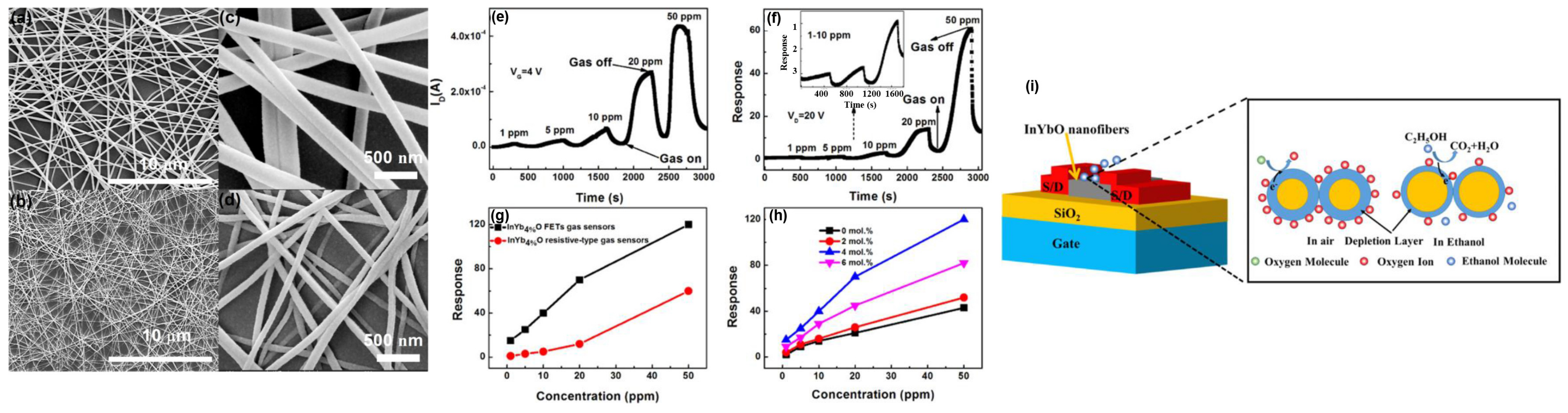
  59. Jun, L.; Chen, Q.; Fu, W.H.; Yang, Y.H.; Zhu, W.Q.; Zhang, J.H. Electrospun Yb–Doped In2O3 Nanofiber Field–Effect Transistors for Highly Sensitive Ethanol Sensors. ACS Appl. Mater. Interfaces 2020, 12, 38425–38434. [Google Scholar] [CrossRef]
  60. Chen, Q.; Li, J.; Fu, W.H.; Yang, Y.H.; Zhu, W.Q.; Zhang, J.H. Detection of N,N–dimethylformamide vapor down to ppb level using electrospun InYbO nanofibers field–effect transistor. Sens. Actuator B–Chem. 2020, 323, 10. [Google Scholar] [CrossRef]
  61. Li, J.; Li, L.K.; Chen, Q.; Zhu, W.Q.; Zhang, J.H. Ultrasensitive room–temperature acetone gas sensors employing green–solvent–processed aligned InNdO nanofiber field–effect transistors. J. Mater. Chem. C 2022, 10, 860–869. [Google Scholar] [CrossRef]
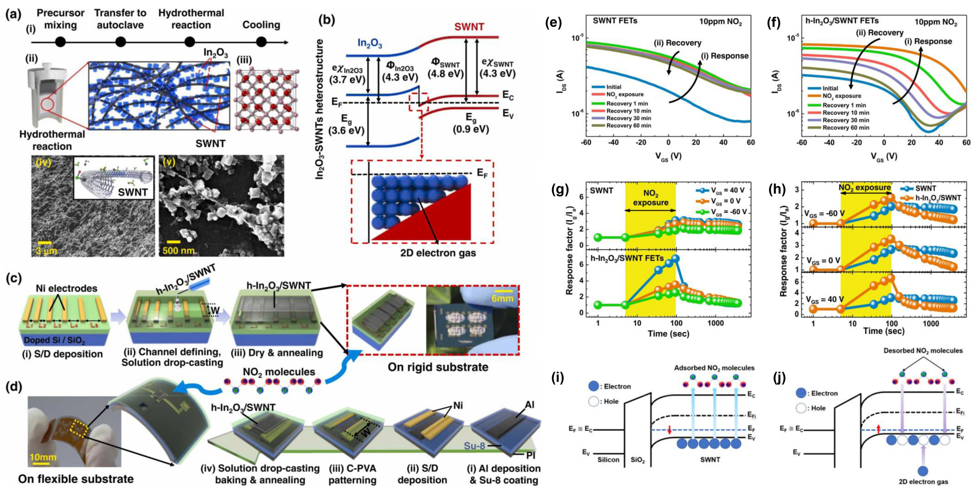
  62. Seo, S.G.; Baek, J.I.; Mishra, D.; Jo, H.; Kwon, H.I.; Jin, S.H. One–pot hydrothermal growth of indium oxide–CNT heterostructure via single walled carbon nanotube scaffolds and their application toward flexible NO2 gas sensors. J. Alloy. Compd. 2022, 922, 11. [Google Scholar] [CrossRef]
  63. Yeom, G.; Kwon, D.; Shin, W.; Park, M.K.; Kim, J.J.; Lee, J.H. Fast–response/recovery In2O3 thin–film transistor–type NO2 gas sensor with floating–gate at low temperature. Sens. Actuator B–Chem. 2023, 394, 9. [Google Scholar] [CrossRef]
  64. Lv, Q.J.; Li, R.F.; Qu, Y.H.; Yu, M.Y.; Zhang, L.; Li, H.H. CeO2 nanorods decorated In2O3nanoparticles for enhanced low temperature detection of hydrogen. Inorg. Chem. Commun. 2023, 158, 9. [Google Scholar] [CrossRef]
  65. Meng, D.; Qiao, T.T.; Ji, Y.; Wang, R.S.; Zhang, Y.; San, X.G.; Jin, Q.; Wang, X.L. Hydrangea–Like In2O3@In2S3 n–n Heterostructures for High–Efficiency TMA Measurement. IEEE Trans. Instrum. Meas. 2023, 72, 9. [Google Scholar] [CrossRef]
  66. An, D.M.; Wang, Y.Y.; Dai, J.L.; Guo, L.P.; Liu, N. Synthesis of Pr doped In2O3 nanoparticles and their enhanced ethanol gas–sensing performance. Ceram. Int. 2024, 50, 4945–4954. [Google Scholar] [CrossRef]
  67. Min, S.K.; Kim, H.S.; Chang, S.P. Highly sensitive toluene sensor based on porous core–shell–structured In2O3–ZnO nanofibers under UV irradiation at room temperature. Phys. E 2023, 154, 13. [Google Scholar] [CrossRef]
  68. Zhu, L.; Wang, J.A.; Liu, J.W.; Wang, Z.; Sun, S.Y.; Li, M.T.; Yan, W. ZIF–L(Co) derived cobalt doped In2O3 hollow nanofibers with high surface activity for efficient formaldehyde gas sensing. Sens. Actuator B Chem. 2024, 403, 9. [Google Scholar] [CrossRef]
  69. Kong, D.L.; Niu, J.Y.; Hong, B.; Xu, J.C.; Han, Y.B.; Peng, X.L.; Ge, H.L.; Li, J.; Zeng, Y.X.; Wang, X.Q. Ag–nanoparticles–anchored mesoporous In2O3 nanowires for ultrahigh sensitive formaldehyde gas sensors. Mater. Sci. Eng. B Adv. Funct. Solid State Mater. 2023, 291, 10. [Google Scholar] [CrossRef]
  70. Zhang, C.Z.; Liu, Y.A.; Wang, C.; Xu, J.Q.; Bai, Y.L. In2O3 decorated Co32 cluster for high performance H2S MEMS sensors. Inorg. Chem. Commun. 2023, 157, 7. [Google Scholar] [CrossRef]
  71. Wang, X.L.; Li, Y.W.; Jin, X.H.; Sun, G.; Cao, J.L.; Wang, Y. The effects of Co doping on the gas sensing performance of In2O3 porous nanospheres. Sens. Actuator B Chem. 2024, 403, 11. [Google Scholar] [CrossRef]
  72. He, T.; Liu, H.C.; Zhang, J.; Yang, Y.P.; Hu, Y.J.; Zhang, Y.; Hu, K.L. DFT study on the adsorption and sensing properties of dissolved gases (H2, CO and CH4) in transformer oil on PdO–doped In2O3 (110) surfaces. Chem. Phys. Lett. 2023, 832, 9. [Google Scholar] [CrossRef]
  73. Liu, Y.P.; Yang, Z.; Huang, L.; Zeng, W.; Zhou, Q. Anti–interference detection of mixed NOX via In2O3–based sensor array combining with neural network model at room temperature. J. Hazard. Mater. 2024, 463, 12. [Google Scholar] [CrossRef] [PubMed]
  74. Zou, X.M.; Wang, J.L.; Liu, X.Q.; Wang, C.L.; Jiang, Y.; Wang, Y.; Xiao, X.H.; Ho, J.C.; Li, J.C.; Jiang, C.Z.; et al. Rational Design of Sub–Parts per Million Specific Gas Sensors Array Based on Metal Nanoparticles Decorated Nanowire Enhancement–Mode Transistors. Nano Lett. 2013, 13, 3287–3292. [Google Scholar] [CrossRef] [PubMed]
  75. Zeng, H.; Takahashi, T.; Kanai, M.; Zhang, G.Z.; He, Y.; Nagashima, K.; Yanagida, T. Long–Term Stability of Oxide Nanowire Sensors via Heavily Doped Oxide Contact. ACS Sens. 2017, 2, 1854–1859. [Google Scholar] [CrossRef] [PubMed]
  76. Kim, T.S.; Lee, Y.; Xu, W.T.; Kim, Y.H.; Kim, M.; Min, S.Y.; Kim, T.H.; Jang, H.W.; Lee, T.W. Direct–printed nanoscale metal–oxide–wire electronics. Nano Energy 2019, 58, 437–446. [Google Scholar] [CrossRef]
  77. Kwon, D.; Jung, G.; Shin, W.; Jeong, Y.; Hong, S.; Oh, S.; Bae, J.H.; Park, B.G.; Lee, J.H. Low–power and reliable gas sensing system based on recurrent neural networks. Sens. Actuator B–Chem. 2021, 340, 11. [Google Scholar] [CrossRef]
  78. Kwon, D.; Jung, G.; Shin, W.; Jeong, Y.; Hong, S.; Oh, S.; Kim, J.; Bae, J.H.; Park, B.G.; Lee, J.H. Efficient fusion of spiking neural networks and FET–type gas sensors for a fast and reliable artificial olfactory system. Sens. Actuator B–Chem. 2021, 345, 9. [Google Scholar] [CrossRef]
  79. Wang, B.; Cancilla, J.C.; Torrecilla, J.S.; Haick, H. Artificial Sensing Intelligence with Silicon Nanowires for Ultraselective Detection in the Gas Phase. Nano Lett. 2014, 14, 933–938. [Google Scholar] [CrossRef]
  80. Royer, J.E.; Kappe, E.D.; Zhang, C.Y.; Martin, D.T.; Trogler, W.C.; Kummel, A.C. Organic Thin–Film Transistors for Selective Hydrogen Peroxide and Organic Peroxide Vapor Detection. J. Phys. Chem. C 2012, 116, 24566–24572. [Google Scholar] [CrossRef]
  81. Ghediya, P.R.; Magari, Y.; Sadahira, H.; Endo, T.; Furuta, M.; Zhang, Y.; Matsuo, Y.; Ohta, H. Reliable Operation in High–Mobility Indium Oxide Thin Film Transistors. Small Methods 2024, 2400578. [Google Scholar] [CrossRef] [PubMed]
  82. Shen, G.; Liang, B.; Wang, X.; Chen, P.C.; Zhou, C. Indium oxide nanospirals made of kinked nanowires. ACS Nano. 2011, 5, 2155–2161. [Google Scholar] [CrossRef] [PubMed]
  83. Singh, N.; Yan, C.; Lee, P.S. Room temperature CO gas sensing using Zn–doped In2O3 single nanowire field effect transistors. Sens. Actuators B Chem. 2010, 150, 19–24. [Google Scholar] [CrossRef]
  84. Huang, W.; Zeng, L.; Yu, X.; Guo, P.; Wang, B.; Ma, Q.; Chang, R.P.H.; Yu, J.; Bedzyk, M.J.; Marks, T.J.; et al. Metal Oxide Transistors via Polyethylenimine Doping of the Channel Layer: Interplay of Doping, Microstructure, and Charge Transport. Adv. Funct. Mater. 2016, 26, 6179–6187. [Google Scholar] [CrossRef]
  85. Zhao, H.; Li, J.; She, X.; Chen, Y.; Wang, M.; Wang, Y.; Du, A.; Tang, C.; Zou, C.; Zhou, Y. Oxygen Vacancy–Rich Bimetallic Au@Pt Core–Shell Nanosphere–Functionalized Electrospun ZnFe2O4 Nanofibers for Chemiresistive Breath Acetone Detection. ACS Sens. 2024, 9, 2183–2193. [Google Scholar] [CrossRef]
  86. Yu, C.; Liu, J.; Zhao, H.; Wang, M.; Li, J.; She, X.; Chen, Y.; Wang, Y.; Liu, B.; Zou, C.; et al. Sensitive Breath Acetone Detection Based on α–Fe2O3 Nanoparticles Modified WO3 Nanoplate Heterojunctions. IEEE Trans. Instrum. Meas. 2024, 73, 1–8. [Google Scholar] [CrossRef]
Figure 1. Recovery assisted by a self–curing method. (a) Diagram of gate oxide degradation due to OSS. (b) ID–VCG versus tOSS. (c) SID/ID2 before and after OSS. (d) VD–IFWD. (e) ID–VCG of OSS and after a self–curing method. (f) SID/ID2 of OSS and after self–curing. Response characteristics of the (g) pristine, (h) OSS–damaged, and (i) self–cured sensors. Reproduced with permission [51]. Copyright 2022, Springer.
Sensors 24 06150 g001
Figure 2. (top graph side) Reconfigurable control of oxygen content. (a) Schematic diagrams illustrating the band structure and electron concentration. (b) Adsorption model of NO2 and H2S. Reproduced with permission [52]. Copyright 2023, American Chemical Society. (bottom graph side) Hydroxy–rich–surface In2O3 gas sensor. (c) Photo of the magnetron RF sputtering. (d) Schematic representation of the sputtering process. (e) Transfer curves of two FET–type gas sensors. (f) Transfer characteristics corresponding to the response to NO2. (g) The response to 500 ppb NO2 versus operating temperature. (h) The response versus NO2 concentration. Reproduced with permission [53]. Copyright 2023, American Chemical Society.
Sensors 24 06150 g002
Figure 3. (top graph side) Si–based FET gas sensor. (a) ID–VG curves and (b) gm–VG curves. (c) Transient responses to NO2 and H2S at fixed Wch/Lch ratio. (d) Transient responses to NO2 and H2S at varying Wch/Lch ratio. Reproduced with permission [54]. Copyright 2023, Elsevier. (bottom graph side) H2S gas sensor based on polysilicon control–gate FET–type gas sensor. ID–VCG1 curves with (e) opened, and (f) grounded VCG2, respectively. (g) ΔID versus VCG1. Reproduced with permission [55]. Copyright 2023, Elsevier.
Sensors 24 06150 g003
Figure 4. FET and resistive gas sensor based on Yb–doped In2O3. SEM images of the (a,c) as–electrospun, and (b,d) annealed 4% Yb–doped In2O3 nanofibers. Dynamic response of the (e) FET, and (f) resistive sensors. (g) Response comparison between the FET and resistive sensors. (h) Response versus Yb doping concentration. (i) Schematic diagram of sensing mechanism. Reproduced with permission [59]. Copyright 2020, American Chemical Society.
Sensors 24 06150 g004
Figure 5. Gas sensing properties of the h–In2O3/SWNT TFT. (a) Preparation process of h–In2O3/SWNT and corresponding SEM images. (i) Preparation process of h–In2O3/SWNT. (ii) Schematic diagram of prepared h–In2O3/SWNT. (iii) The cubic crystal structure of h–In2O3/SWNT. SEM images of (iv) pure SWNTs and (v) h–In2O3/SWNT. (b) Band structure. Fabrication of gas sensors on the rigid (c) and flexible (d) substrates. Transfer characteristics of (e) SWNT FETs and (f) h–In2O3/SWNT FETs with response to NO2. (g) Response values obtained at dynamic measurements. (h) Comparison of response values to different VGS. Band structures’ diagrams of NO2 (i) response and (j) recovery. Reproduced with permission [62]. Copyright 2022, Elsevier.
Sensors 24 06150 g005
Figure 6. Influence of the deposition rate on signal–to–noise ratio. (ac) Schematic diagram of resistive and FET sensors. (d) Deposition rate versus the RF sputtering power. (e) Resistivity versus the RF sputtering power. (f) The signal–to–noise ratio versus H2S concentration. (g) The signal–to–noise ratio per unit channel area versus the RF sputtering power. Reproduced with permission [47]. Copyright 2020, Royal Society of Chemistry.
Sensors 24 06150 g006
Figure 7. Characteristics of low–frequency noise for In2O3–based gas sensors. (a) Transfer characteristics of the resistive sensors in response to 50 ppm H2S. (b) The normalized low–frequency noise spectra of the resistive sensors with response to 50 ppm H2S. (c) Transfer characteristics of the FET sensors in response to 50 ppm H2S. (d) The normalized low–frequency noise spectra of the FET sensors with response to 50 ppm H2S. Reproduced with permission [48]. Copyright 2020, Elsevier.
Sensors 24 06150 g007
Figure 8. (a) Schematic of gas sensing and low–frequency noise measurement system. (b) Signal–to–noise ratio versus NO2 concentrations at logarithmic scale. Reproduced with permission [49]. Copyright 2021, Elsevier.
Sensors 24 06150 g008
Figure 9. Si MOSFET gas sensor based on Pt–In2O3 with reduced recovery time. (a) The manufactured MOSFET’s transient CO response versus Pt concentration. (b) The transient CO response of the 5 wt% Pt–In2O3 sensor versus temperature. (c) The transient CO response of the 5 wt% Pt–In2O3 sensor versus Vpre. (d) Pre–bias measuring pulse scheme. (e) Response values and recovery times versus Vpre. (f) Enhanced response and recovery process by Vpre. Reproduced with permission [46]. Copyright 2019, Elsevier.
Sensors 24 06150 g009
Figure 10. The Nd–doped In2O3 FET–based acetone sensor. (a) The electrospinning schematic diagram. (b) The correlation between specific surface area of InNdO nanofibers and Nd doping concentration. (c) Oxygen vacancy concentrations for varying Nd contents. (d) Transfer characteristics versus Nd doping concentrations. (e) The InNd3%O nanofiber FETs’ dynamic response. (f) Response and recovery times versus acetone concentrations. Reproduced with permission [61]. Copyright 2022, Royal Society of Chemistry.
Sensors 24 06150 g010
Figure 11. Fast response/recovery NO2 sensor based on In2O3 TFT. Diagram of the NO2 gas detecting system in the (a) program and (b) erase states. (c) Response and recovery behaviors versus ΔVth. (d) Response and (e) recovery behaviors versus ID. (f) The PBR method’s pulse scheme. (g) Recovery behaviors versus VPBR. Reproduced with permission [63]. Copyright 2023, Elsevier.
Sensors 24 06150 g011
Figure 12. Physisorption in an oxygen sensor of the high–performance In2O3 FET type operating at room temperature. (a) Dynamic response of 30% O2. (b) Sensitivities versus temperature. (c) Dynamic response of 30% O2 with ∼21% O2 set as the reference gas. Reproduced with permission [45]. Copyright 2018, Royal Society of Chemistry.
Sensors 24 06150 g012
Figure 13. (left graph side) (a) Diagram illustrating the sensor configuration for the “one lock to one key” design concept. (b) Hybrid Mg–doped In2O3 NW FETs decorated with Au, Ag, and Pt nanoparticles, respectively. (c) The sensitivity of three FETs decorated with Au, Ag, and Pt nanoparticles in response to different gases. Reproduced with permission [74]. Copyright 2013, American Chemical Society. (right graph side) (d) Preparation of electrospinning. (e) SEM images of Yb–doped nanofibers before and after the annealed process. (f) Transient response of the Yb–doped In2O3 TFT towards different gases. (g) The selectivity of the sensor. Reproduced with permission [60]. Copyright 2020, Elsevier.
Sensors 24 06150 g013
Figure 14. Long–term stability improved by replacing traditional metal contacts with heavily doped metal oxides. (a) Diagram of reasons for improved long–term stability. I–V curves of (b) Ti and (c) ATO contact devices. (d) The resistivity of metal oxide nanowires versus the aging time. (e) The contact resistance of metal oxide nanowires versus the aging time. The sensor response towards NO2 versus after 186 h aging of (f) Ti and (g) ATO contact devices. (h) The varying response values that change over aging time. Reproduced with permission [75]. Copyright 2017, American Chemical Society.
Sensors 24 06150 g014
Figure 15. Diagram of the nanoscale MOW circuits printed directly on substrate. (a) Printing under digital control. (b) Metal oxide nanowire FET. (c) Transparent metal oxide nanowire FET. (d) All metal oxide nanowire FET. (e) Metal oxide nanowire synaptic transistors. (f) Metal oxide nanowire gas sensors. Reproduced with permission [76]. Copyright 2019, Elsevier.
Sensors 24 06150 g015
Figure 16. (left graph side) (a) Predicted concentration for NO2 and H2S utilizing the RNN train over 500 epochs compared to the target concentration. Reproduced with permission [77]. Copyright 2021, Elsevier. (right graph side) (b) Predicted H2S and NO2 concentrations through SNNs. Reproduced with permission [78]. Copyright 2021, Elsevier.
Sensors 24 06150 g016
Table 1. In2O3 transistors with high mobility.
TypePreparation MethodMobility/μ
cm2v−1s−1
Refs.
Commercial IGZO thin filmPVD10/
Unpassivated In2O3 thin filmPVD85[81]
In2O3 nanowiresCVD>200[82]
Zn–doped In2O3 nanowiresCVD139[83]
PVA–doped In2O3 thin filmSolution processed4[84]
PEI–doped In2O3 thin filmSolution processed9[84]
Disclaimer/Publisher’s Note: The statements, opinions and data contained in all publications are solely those of the individual author(s) and contributor(s) and not of MDPI and/or the editor(s). MDPI and/or the editor(s) disclaim responsibility for any injury to people or property resulting from any ideas, methods, instructions or products referred to in the content.

