Article

Noise Analysis and Suppression Methods for the Front-End Readout Circuit of a Microelectromechanical Systems Gyroscope

1
School of Computer, Guangdong University of Technology, Guangzhou 510006, China
2
Science and Technology on Reliability Physics and Application Technology of Electronic Component Laboratory, China Electronic Product Reliability and Environmental Testing Research Institute, Guangzhou 511370, China
3
National Key Laboratory of Science and Technology on Micro/Nano Fabrication, Institute of Microelectronics, Peking University, Beijing 100871, China
*
Authors to whom correspondence should be addressed.
Sensors 2024, 24(19), 6283; https://doi.org/10.3390/s24196283
Submission received: 8 August 2024 / Revised: 18 September 2024 / Accepted: 25 September 2024 / Published: 28 September 2024
(This article belongs to the Special Issue Smart Sensors and Integration Technology for MEMS Devices)

Abstract

:
Circuit noise is a critical factor that affects the performances of an MEMS gyroscope. Therefore, it is essential to analyze and suppress the noises in the key analog circuits, which are the main noise sources. This study presents an optimized front-end readout circuit and noise suppression methods. First, the noise analysis of the front-end readout circuit is carried out with theoretical derivation to clarify the main noise contributors. To suppress the output noise, an improved readout circuit based on the T-resistor networks is proposed, and the corresponding noise equation is derived in detail. In addition, the noise analysis of the critical circuits of the detection and control system, such as the inverting amplifiers, the first-order low-pass filters, and the first-order high-pass filters, is carried out, and the noise suppression strategy with the optimization of the resistances and is proposed. Taking the inverting amplifier as an example, the theoretical derivation is verified by measuring and comparing the output noises of different resistance schemes. In addition, the output noises of the gyroscope before and after circuit optimization are measured. Experimental results demonstrate that the output noise with the circuit optimization is reduced from 60 μV/Hz1/2 to 30 μV/Hz1/2 and the bias instability is reduced from 3.8 deg/h to 1.38 deg/h. In addition, the ARW is significantly improved from 0.035 deg/h1/2 to 0.018 deg/h1/2, which indicates that the proposed noise analysis and suppression methods are effective and feasible.

1. Introduction

A microelectromechanical systems (MEMS) gyroscope is a crucial component of an inertial measurement unit (IMU) [1,2]. Nowadays, industrial robots, drones, unmanned vehicles, and other intelligent terminals with IMUs have been widely developed and applied in industrial production and social life. For unmanned terminals, localization and attitude sensing provide basic motion information for their operation and control [3,4]. In particular, the MEMS gyroscope provides the angular velocity for attitude recognition and combined navigation [5]. When a gyroscope vibrating along the x-axis rotates around the z-axis with a certain angular velocity, a Coriolis force will be generated, causing the mass block to vibrate along the y-axis [6,7]. The distance between the detection electrode and the mass block varies proportionally to the angular velocity, causing a change in the capacitance [8]. Therefore, the angular velocity can be calculated by detecting the small capacitance change with a front-end readout circuit [9,10].
In IMUs, circuit noise is an important factor that affects and limits gyroscopes’ performances [11,12,13]. Noise mainly includes 1/f noise, shot noise, Johnson noise, mechanical thermal noise, etc. [14,15]. Noise is a random signal that interferes with the useful signals of the detection and control system. When the signal-to-noise ratio (SNR) is low, the useful signals may be significantly disrupted or even overwhelmed by the noise [16]. Since voltage and current noise are stochastic, it is essential to select a suitable statistical method for noise analysis and evaluate their impacts on the gyroscope’s performances. In general, the distribution of random signal energy can be characterized through the power spectral density (PSD) [17]. Additionally, nonsmooth noise can be differential processed to achieve smoothing [18]. The magnitude of the noise can be estimated with the mean squared error (MSE), and Allan variance can be utilized to effectively separate noise sources, particularly for nonstationary stochastic processes [19,20].
After identifying the main noise contributors, it is necessary to adopt appropriate measures to suppress the noises. Currently, noise reduction techniques can be classified as either preprocessing techniques or post-processing techniques. Preprocessing techniques are mainly realized by optimizing the circuit structure, resistance, capacitance, and chip selection, which can suppress the noise from the source [21,22,23]. For example, Mengxiang Liu et al. designed a two-stage charge amplifier instead of a transimpedance amplifier, which greatly reduces the input current noise and the overall phase shift of the loop introduced by the transimpedance [24]. Feng Bu et al. developed a noise model for force-to-rebalance closed-loop detection by analyzing the transfer path of electro-feedback noise in the electromechanical amplitude modulation detection circuit of an MEMS gyroscope. After noise optimization, the angle random walk (ARW) was reduced from 0.148°/√h to 0.017°/√h, improving performance by about 8.7 times [25]. Guoming Xia et al. implemented a high-precision frequency readout method and CMOS integrated circuit for a vibrating beam accelerometer using the sigma-delta modulation. This method has the advantages of low quantization noise, large measuring range, and high linearity [26].
For post-processing techniques, adaptive filtering, Kalman filtering, wavelet transform, artificial neural network, and support vector machine can be used for noise reduction [27,28,29,30]. For instance, Ning Liu et al. proposed a nonlinear suppression method based on cubic Kalman filter-phase space reconstruction (CKF-PSR), which is used to compensate random noise in real time [31]. However, there are difficulties in hardware implementation. An autoregressive Kalman-filter-based model for gyroscope long-term error (LTE) was proposed by Javad Abbasi et al., reducing the zero-bias instability by 50% and the measurement error by 4%~70% [32]. Moreover, the effect of ambient temperature on the performances such as bias instability and scale factor should not be neglected [33,34,35]. In general, high vacuum encapsulation can reduce the air damping and improve the quality factor and mechanical sensitivity. This results in a noise reduction in the detection circuits and control system [36]. In addition, drive closed-loop control techniques such as active gain control (AGC) and phase-locked loop control (PLL) are used to enhance full-temperature control capability [37].
In summary, the weak signals detected by the readout circuits of gyroscopes are inevitably influenced by ambient temperature, mechanical structure, and circuit noises [38]. Noises significantly influence the gyroscope’s mechanical sensitivity, angle random walk, and bias instability [39,40]. In our previous work, an electrical coupling suppression and closed-loop control method was proposed to improve the performance, and the bias instability reached 6.3 deg/h without noise analysis and optimization [41]. However, it can be further advanced by noise analysis and optimization. Therefore, it is essential to analyze the noise contributors in detail and suppress noises from both physical and mathematical perspectives. In [41], the detection and control system was based on both analog and digital circuits, and the analog circuits mainly included the front-end readout circuit, inverting amplifiers, low-pass filters, and high-pass filters, while the digital circuits mainly included the analog to digital converters (ADCs), digital to analog converters (DACs), and field-programmable gate array (FPGA). Given that noises mainly result from the analog circuits, in this paper, the noise analysis and optimization of the key analog circuits will be conducted. Compared with the previous work, this work provides a detailed derivation and analysis of noise in commonly used analog circuits, and integrates methods such as chip selection, circuit structural optimization, and parameter optimization to suppress noise, thus effectively improving the key performance of MEMS gyroscopes.

2. Theoretical Analyses

The analog circuits of the drive mode are similar to those of the sense mode; thus, in this work, the analog circuits of the drive mode are taken as the example for analysis.

2.1. Noise Analysis of the Readout Circuit

In [41], the front-end readout circuit with feed-forward coupling compensation control is illustrated in Figure 1. VL and VR are differential drive signals, and Cs1 and Cs2 are the differential detection capacitor. Their equations can be depicted as (1).
V R = V d c + V a c sin ( ω d t ) V L = V d c V a c sin ( ω d t ) C s 1 = N s ε h l d 0 N s ε h A d d 0 cos ( ω d t ) C s 2 = N s ε h l d 0 + N s ε h A d d 0 cos ( ω d t )
where ωd is the resonant frequency of the drive mode, and t is the time. Ns is the number of detection capacitors, and ε is the dielectric constant. h is the thickness, l is the initial length, and d0 is the spacing of the combs. Ad is the amplitude of the drive displacement. When the quality factor Qd is very large, Ad is approximately equal to F0Qd/mdωd2. md is the drive mass and F0 is the amplitude of the drive force. Vac is the amplitude of the drive alternating current (AC) signal, and Vdc is the amplitude of the drive direct current (DC) signal.
Cp1 and Cp2 are the parasitic capacitors between the drive and sense combs, while Cpc is the coupling compensation capacitor. Vpc is the coupling compensation AC voltage, which is equal to KpcVacsin(ωdt). Cf1 and Cf2 are the feedback capacitors, while Rf1 and Rf2 are the feedback resistors of the two transimpedance amplifiers. Capacitors Ch1 and Ch2, and resistors Rh1 and Rh2 are applied to construct a first-order passive high-pass filter (HPF) to filter the low-frequency signal. Rg is the resistor of the instrumentation amplifier to set a gain of kg. For avoiding the output saturation of the instrumentation amplifier, the HPF composed of C3, R3, and R0 is used to eliminate the DC signal.
Assuming that Cf1 = Cf2 = Cf, Rf1 = Rf2 = Rf, Cp1 = Cp2 = Cp, Ch1 = Ch2 = Ch, Rh1 = Rh2 = Rh, and 1 << ωdChRh, the output voltage VA, VB, and VAVB can be calculated as (2).
V A ( s ) = s R f 1 ( C s 1 V C + C p 1 V L + C p c V p c ) 1 + s R f 1 C f 1 × s R h 1 C h 1 1 + s R h 1 C h 1 V B ( s ) = s R f 2 ( C s 2 V C + C p 2 V R ) 1 + s R f 2 C f 2 × s R h 2 C h 2 1 + s R h 2 C h 2 V B ( s ) V A ( s ) s R f [ ( C s 1 C s 2 ) V C + C p ( V L V R ) + C p c V p c ] 1 + s R f C f s R f [ ( K p c C p c 2 C p ) V a c sin ( ω d t ) 2 V C N s ε h A d d 0 cos ( ω d t ) ] 1 + s R f C f
where complex frequency s is equal to , and ω stands for the angular frequency. VC is the DC carrier. Given that the front-end readout circuit adopts the velocity detection scheme, 1 >> ωdCfRf. In addition, due to the HPF added to the instrumentation amplifier, 1 << ωdC3R3. The electrical coupling signals induced by Cp1 and Cp2 can be effectively suppressed by compensation capacitor Cpc, as long as KpcCpc = 2Cp, as shown in (2). Thus, the output voltage Vout1(s) can be derived as (3), and the time-domain signal Vout1 and its root mean square (RMS) value VRMS1 can be obtained as (4).
V o u t 1 ( s ) = k g ( V B V A ) × s R 3 C 3 1 + s R 3 C 3 2 s k g R f V C N s ε h A d d 0 cos ( ω d t )
V o u t 1 = 2 k g R f V C N s ε h F 0 Q d d 0 m d ω d sin ( ω d t ) V R M S 1 = 2 k g R f V C N s ε h F 0 Q d d 0 m d ω d
The noise analysis schematic of the front-end readout circuit is shown in Figure 2, where Vn_Op1 and Vn_Op2 are the input noise voltages at the negative end of the two operational amplifiers, In_Op1 is the input noise current at the positive end of the operational amplifier, In_On1 and In_On2 are the input noise currents at the negative end of the two operational amplifiers, Vn_Da is the input noise voltage of the instrumentation amplifier, In_Dap and In_Dan are the input noise currents at the positive and negative ends of the instrumentation amplifier, and Vn_Rg, Vn_R3, Vn_R0, Vn_Rf1, Vn_Rf2, Vn_Rh1, and Vn_Rh2 are the noise voltages of resistors Rg, R3, R0, Rf1, Rf2, Rh1, and Rh2, respectively. Based on the definition of Johnson noise, the PSDs of their noise are derived as (5). Thus, the PSDs of the output noise voltage of the two transimpedance amplifiers can be derived as (6). Since the noises of the two transimpedance amplifiers are uncorrelated, the PSD of the output noise voltage of the instrument amplifier can be derived as (7). Assuming that In_Dap = In_Dan = In_Da, Vn_Op1 = Vn_Op2 = Vn_Op, In_On1 = In_On2 = In_On, In_Op1 = In_Op2 = In_Op, and considering the noise at the resonant frequency ωd, then (6) and (7) can be simplified to (8) and (9), respectively.
V n _ R g Δ f = 4 k b T R g , V n _ R 3 Δ f = 4 k b T R 3 , V n _ R 0 Δ f = 4 k b T R 0 , V n _ R f 1 Δ f = 4 k b T R f 1 , V n _ R f 2 Δ f = 4 k b T R f 2 , V n _ R h 1 Δ f = 4 k b T R h 1 , V n _ R h 2 Δ f = 4 k b T R h 2
V n _ a 1 2 Δ f = 4 k b T R f 1 1 + ω 2 R f 1 2 C f 1 2 + I n _ O n 1 2 R f 1 2 1 + ω 2 R f 1 2 C f 1 2 + V n _ O p 1 2 [ 1 + ω 2 R f 1 2 ( C f 1 + C s 1 + C p 1 + C p c ) 2 ] 1 + ω 2 R f 1 2 C f 1 2 V n _ b 1 2 Δ f = 4 k b T R f 2 1 + ω 2 R f 2 2 C f 2 2 + I n _ O n 2 2 R f 2 2 1 + ω 2 R f 2 2 C f 2 2 + V n _ O p 2 2 [ 1 + ω 2 R f 2 2 ( C f 2 + C s 2 + C p 2 ) 2 ] 1 + ω 2 R f 2 2 C f 2 2
V n 1 2 Δ f = V n 10 2 Δ f ω 2 R 3 2 C 3 2 1 + ω 2 R 3 2 C 3 2 + 1 + ω 2 R 3 2 C 3 2 ω 2 R 3 2 C 3 2 ( 4 k b T R 0 + I n _ O p 1 2 R 0 2 + V n _ O p 1 2 ) + 4 k b T R 3 ω 2 R 3 2 C 3 2 + I n _ O n 1 2 ω 2 C 3 2 V n 10 2 Δ f = k g 2 [ V n _ a 1 2 Δ f ω 2 R h 1 2 C h 1 2 1 + ω 2 R h 1 2 C h 1 2 + V n _ b 1 2 Δ f ω 2 R h 2 2 C h 2 2 1 + ω 2 R h 2 2 C h 2 2 + 4 k b T R h 1 1 + ω 2 R h 1 2 C h 1 2 + 4 k b T R h 2 1 + ω 2 R h 2 2 C h 2 2 + I n _ D a n 2 R h 1 2 1 + ω 2 R h 1 2 C h 1 2 + I n _ D a p 2 R h 2 2 1 + ω 2 R h 2 2 C h 2 2 + V n _ D a 2 + 4 k b T R g ]
V n _ a 1 2 Δ f 4 k b T R f 1 + I n _ O n 1 2 R f 1 2 + V n _ O p 1 2   = 4 k b T R f + I n _ O n 2 R f 2 + V n _ O p 2 V n _ b 1 2 Δ f 4 k b T R f 2 + I n _ O n 2 2 R f 2 2 + V n _ O p 2 2   = 4 k b T R f + I n _ O n 2 R f 2 + V n _ O p 2
V n 1 2 Δ f = V n 10 2 Δ f + ( 4 k b T R 0 + I n _ O p 2 R 0 2 + V n _ O p 2 ) + 4 k b T R 3 ω d 2 R 3 2 C 3 2 + I n _ O n 2 ω d 2 C 3 2 V n 10 2 Δ f = k g 2 [ 2 × ( 4 k b T R f + I n _ O n 2 R f 2 + V n _ O p 2 + 4 k b T ω d 2 R h C h 2 + I n _ D a 2 ω d 2 C h 2 ) + V n _ D a 2 + 4 k b T R g ]
Here, R0 is a matching resistor. Due to the inevitable input offset current in the operational amplifier, it is necessary to make the DC channel resistance at both ends of the operational amplifier equal, namely, R0 = R3, so as to balance the input bias current. Fortunately, the operational amplifier is applied to construct an HPF; thus, the mismatch caused by the input bias current can be filtered by the subsequent HPF and the signal demodulation. Therefore, R0 should be set to 0 to minimize the output noise shown in (9). Thus, (9) can be simplified to (10).
V n 1 Δ f = k g 2 [ 2 × ( 4 k b T R f + I n _ O n 2 R f 2 + V n _ O p 2 + 4 k b T ω d 2 R h C h 2 + I n _ D a 2 ω d 2 C h 2 ) + V n _ D a 2 + 4 k b T R g ] + V n _ O p 2 + 4 k b T R 3 ω d 2 R 3 2 C 3 2 + I n _ O n 2 ω d 2 C 3 2
To further suppress the circuit noise, it is necessary to select precision operational amplifiers and instrumentation amplifiers with high bandwidth, high slew rate, and low noise, so as to minimize the PSDs of input noise voltage and current. In [41], OP2177 and AD8221 are selected as the operational amplifiers and instrumentation amplifier, respectively. They are both powered by Analog Devices, Inc., Norwood, MA, USA. The bandwidth of OP2177 is 1.3 MHz, the slew rate is 0.7 V/μs, the input voltage noise density is 7.9 nV/√Hz, and the input current noise density is 0.2 pA/√Hz. The bandwidth gain product of AD8221 is 0.825 MHz, the slew rate is 2 V/μs, the input voltage noise density is 8 nV/√Hz, and the input current noise density is 6 pA/√Hz. However, they are not the best chips, and they can be replaced by AD8676 and AD8421, respectively. These two chip are also both powered by Analog Devices, Inc., USA. The bandwidth of AD8676 is 10 MHz, the slew rate is 2.5 V/μs, the input voltage noise density is 2.8 nV/√Hz, and the input current noise density is about 0.2 pA/√Hz. The bandwidth gain product of AD8221 is 10 MHz, the slew rate is 35 V/μs, the input voltage noise density is 3 nV/√Hz, and the input current noise density is 0.2 pA/√Hz. It is obvious that chip selection is very important.
In addition, for suppressing the noise, ωd, Ch, and Rh should be increased appropriately, while kg, Rg, and Rf should be decreased. Considering that Rg and kg are inversely proportional, they cannot be increased or decreased simultaneously. If kg and Rf are reduced, the gain of the signal will be also decreased. Here, AD8676 and AD8421 are selected, that is, In_On = 0.2 pA/√Hz, Vn_Op = 2.8 nV/√Hz, In_Da = 0.2 pA/√Hz, and Vn_Da = 3 nV/√Hz. In addition, kb = 1.38 × 10⁻²³ J/K, T = 300 K, ωd = 2π × 8410.6 rad/s, Rf = 1 MΩ, Cf = 1 pF, Rh = 200 kΩ, Ch = 0.01 μF, Rg = 100 Ω. Based on (10) and data calculation, it is clear that the first two terms are the main noises, which are much larger than the other terms. Thus, (10) can be simplified to (11).
V n 1 Δ f k g 2 × ( 4 k b T R f + I n _ O n 2 R f 2 )
Therefore, based on (4) and (11), the signal-to-noise ratio SNR1 of the front-end readout circuit can be obtained as (12).
S N R 1 = V R M S 1 V n 1 Δ f V C N s ε h F 0 Q d d 0 m d ω d 4 k b T / R f + I n _ O n 2
It is obvious that to improve the SNR of the front-end readout circuit, VC, h, F0, Qd, and Rf should be appropriately increased, while d0, md, ωd, and In_On should be reduced. Therefore, in addition to optimizing the structural design and selecting the precise operational amplifier, it is also necessary to set the feedback resistance Rf reasonably. Here, circuit improvement can be achieved with the T-type resistor networks, which can further suppress the noise and advance the SNR.

2.2. An Improved Readout Circuit Based on the T-Resistor Networks

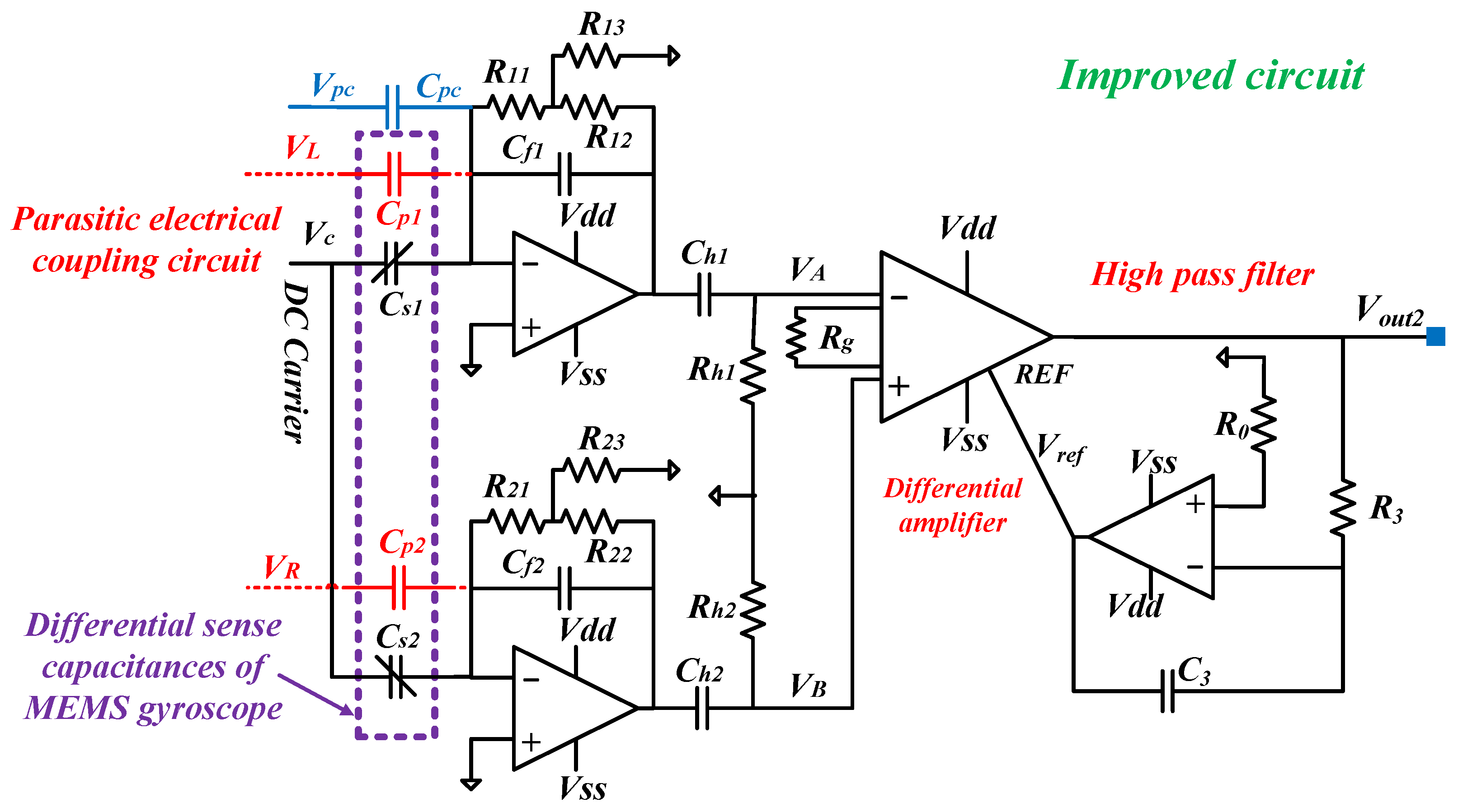
The readout circuit is improved by the T-resistor networks, as shown in Figure 3. Assuming that R11 = R21, R12 = R22, and R13 = R23, then the output voltage Vout2 and its root mean square (RMS) value VRMS2 can be similarly calculated as (13).
V o u t 2 = 2 k g R f f V C N s ε h F 0 Q d d 0 m d ω d sin ( ω d t ) V R M S 2 = 2 k g R f f V C N s ε h F 0 Q d d 0 m d ω d
where Rff = R11 + R12 + R11R12/R13. Given that the front-end readout circuit adopts the velocity detection scheme, 1 >> ωdCfRff. Assuming that R11 = 100 kΩ, R12 = 1 kΩ, R13 = 110Ω, then Rff ≈ 1 MΩ = Rf. It means that the improved circuit and the original circuit have the same transimpedance.
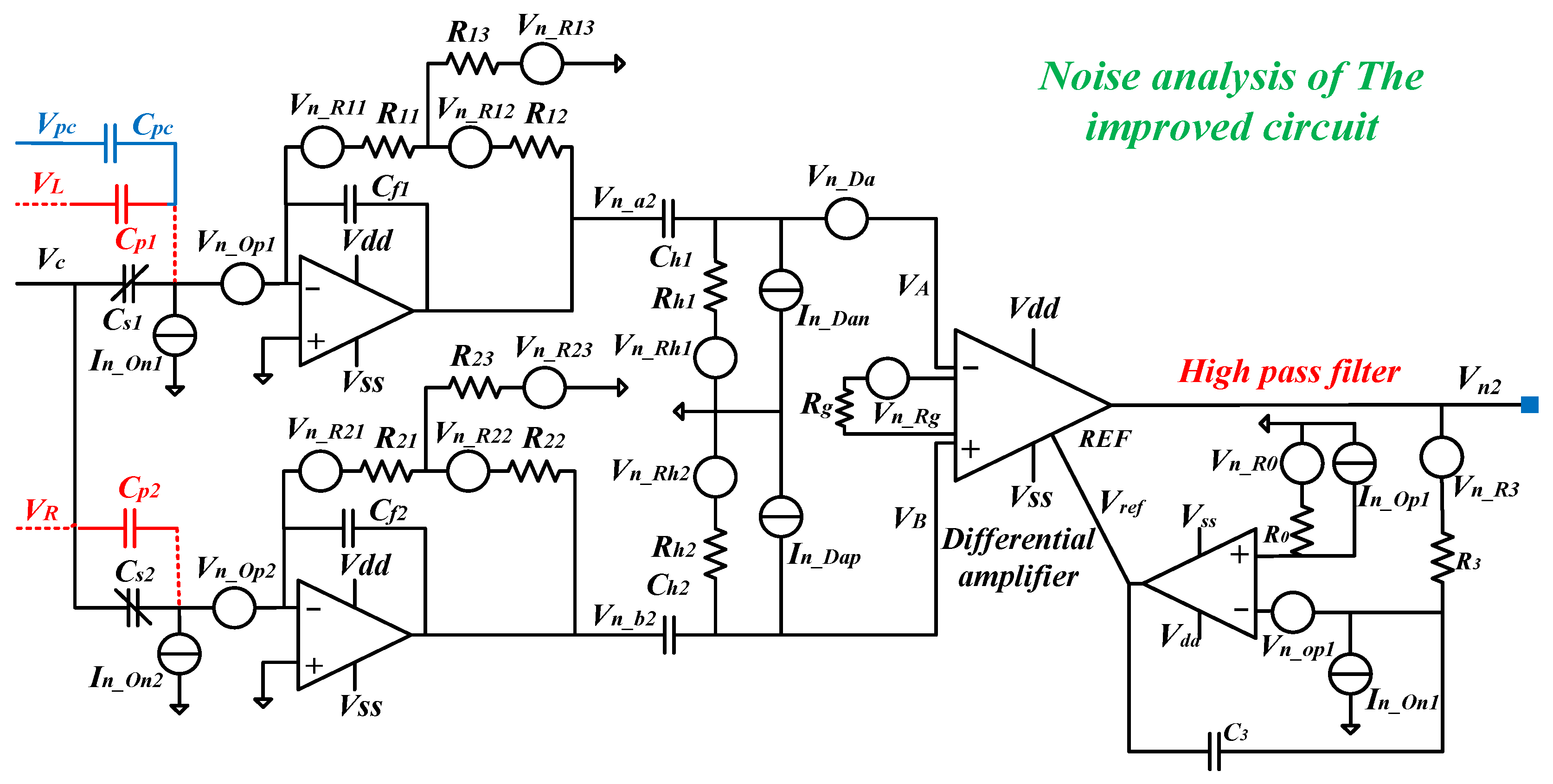
The noise analysis schematic of the improved front-end readout circuit is shown in Figure 4. The noise analysis and derivation are similar to those above. Thus, the PSD of the output noise voltage of the upper transimpedance amplifier can be derived as (14).
V n a 2 2 Δ f = I n _ O n 1 2 R f f 2 1 + ω 2 R f f 2 C f 1 2 + 4 k b T R 11 ( 1 + R 11 / R 13 ) 2 + ω 2 R f f 2 C f 1 2 + 4 k b T R 12 1 + ω 2 R 12 2 C f 1 2 + 4 k b T R 13 ( 1 + R 13 / R 11 ) 2 + ω 2 ( R 13 + R 12 + R 13 R 12 / R 11 ) 2 C f 1 2 + V n _ O p 2 [ ( 1 + R 12 R 13 ) 2 + ω 2 R f f 2 ( C f 1 + C s 1 + C p 1 + C p c ) 2 ] 1 + ω 2 R f f 2 C f 1 2
Similarly, considering the noise at the resonant frequency ωd, then the (14) can be simplified as (15).
V n a 2 2 Δ f 4 k b T ( R 13 2 / R 11 + R 13 + R 12 ) + I n _ O n 2 R f f 2 + V n _ O p 2 R 12 2 / R 13 2
Likewise, the PSD of the output noise voltage of the lower transimpedance amplifier can be derived as (16).
V n b 2 2 Δ f 4 k b T ( R 13 2 / R 11 + R 13 + R 12 ) + I n _ O n 2 R f f 2 + V n _ O p 2 R 12 2 / R 13 2
Thus, the PSD of the output noise voltage of the instrument amplifier can be derived as (17).
V n 2 2 Δ f = V n 20 2 Δ f + ( 4 k b T R 0 + I n _ O p 2 R 0 2 + V n _ O p 2 ) + 4 k b T R 3 ω d 2 R 3 2 C 3 2 + I n _ O n 2 ω d 2 C 3 2 V n 20 2 Δ f = k g 2 { 2 × [ 4 k b T ( R 13 2 / R 11 + R 13 + R 12 ) + I n _ O n 2 R f f 2   + V n _ O p 2 R 12 2 / R 13 2 + 4 k b T ω d 2 R h C h 2 + I n _ D a 2 ω d 2 C h 2 ] + V n _ D a 2 + 4 k b T R g }
Likewise, R0 should be set to 0 to minimize the output noise shown in (9). Thus (17) can be simplified to (18).
V n 2 Δ f = k g 2 { 2 × [ 4 k b T ( R 13 2 / R 11 + R 13 + R 12 ) + I n _ O n 2 R f f 2 + V n _ O p 2 R 12 2 / R 13 2 + 4 k b T ω d 2 R h C h 2 + I n _ D a 2 ω d 2 C h 2 ] + V n _ D a 2 + 4 k b T R g } + V n _ O p 2 + 4 k b T R 3 ω d 2 R 3 2 C 3 2 + I n _ O n 2 ω d 2 C 3 2
After calculation, it is clear that the first two terms are the main noises, which are much larger than the other terms. Thus, (18) can be simplified to (19).
V n 2 Δ f k g 2 × [ 4 k b T ( R 13 2 / R 11 + R 13 + R 12 ) + I n _ O n 2 R f f 2 ]
Therefore, based on (13) and (19), the signal-to-noise ratio SNR2 of the front-end readout circuit can be obtained as (20).
S N R 2 = V R M S 2 V n 2 Δ f V C N s ε h F 0 Q d / ( d 0 m d ω d ) 4 k b T ( R 13 2 / R 11 + R 13 + R 12 ) / R f f 2 + I n _ O n 2
From (4) and (13), the gain of the improved circuit with T-resistor networks remains unchanged. However, from (12) and (20), the SNR of the improved circuit has been advanced because ( R 13 2 / R 11 + R 13 + R 12 ) / R f f 2 R 12 / R f f 2 < 1 / R f f . In addition, the T-resistor network can achieve a high feedback resistance using only three resistors with small resistances, and a single resistor with a very high resistance is hard to achieve. Thus, the noise analysis above figures out that the improved circuit with T-resistor networks are effective to reduce the circuit noise.

2.3. Noise Analysis of the Other Critical Circuits

Given the importance of the inverting amplifier, first-order high-pass filter, and first-order low-pass filter (LPF) in the front-end readout circuit, it is imperative to give careful consideration to the noises induced by these circuits.
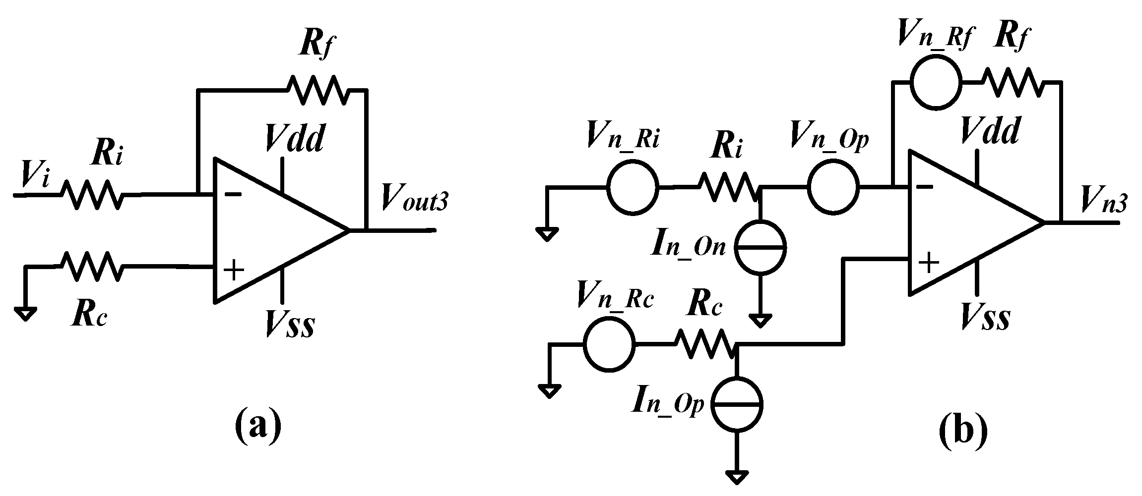
The circuit schematic and noise analysis schematic of the inverting amplifier are illustrated in Figure 5a,b, respectively. Based on the circuits, the gain and output noise can be derived as (21) and (22).
V o u t 3 V i = R f R i
V n 3 2 Δ f = ( 1 + R f / R i ) 2 ( 4 k b T R c + I n _ O p 2 R c 2 + V n _ O p 2 ) + 4 k b T R f + 4 k b T R i ( R f / R i ) 2 + I n _ O n 2 R f 2
where Vout3 and Vn3 are the output voltage and noise voltage of the inverting amplifier, respectively. Rc is a matching resistor. Due to the inevitable input offset current in the operational amplifier, it is necessary to make the DC channel resistance at both ends of the operational amplifier equal, namely, Rc = Ri//Rf, so as to balance the input bias current. Fortunately, the mismatch caused by the input bias current can be filtered by the subsequent HPF and the signal demodulation. Therefore, Rc should be set to 0 to minimize the output noise. Thus, the SNR can be obtained as (23).
S N R 3 = V o u t 3 V n 3 Δ f = V i 4 k b T ( R i + R i 2 / R f ) + ( 1 + R i / R f ) 2 V n _ O p 2 + R i 2 I n _ O n 2
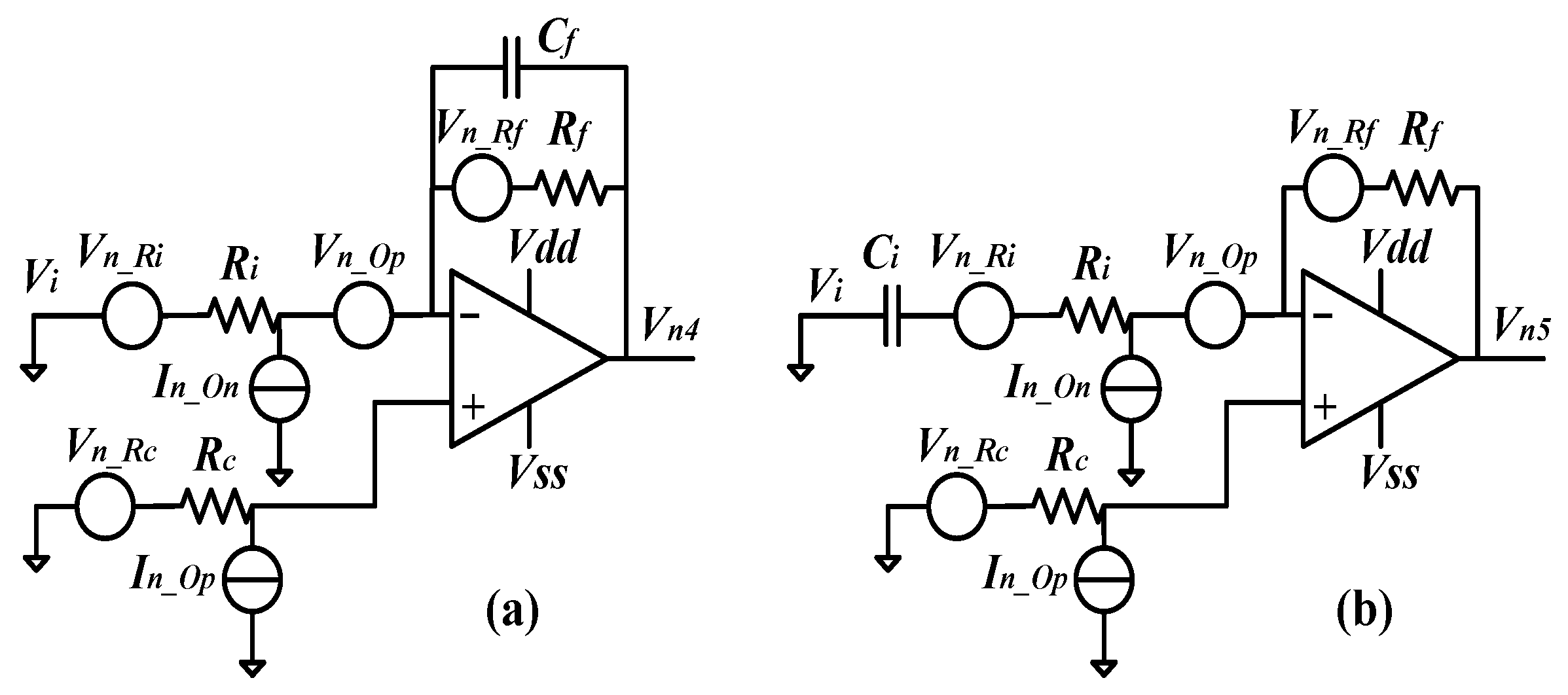
Similarly, the noise analysis schematics of the first-order LPF and the first-order HPF are shown in Figure 6a,b. For the LPF, the transfer function and the PSD of the output noise voltage can be obtained as (24) and (25), respectively. Likewise, to suppress the noise, Rc should be set to 0. If the noise within the passband is considered, thus 1 >> ωCfRf, and the simplified SNR can be obtained as (26).
V o u t 4 V i = R f / R i 1 + s R f C f
V n 4 2 Δ f = 4 k b T R f 1 + ω 2 R f 2 C f 2 + 4 k b T R i ( R f / R i ) 2 1 + ω 2 R f 2 C f 2 + I n _ O n 2 R f 2 1 + ω 2 R f 2 C f 2 + ( 1 + R f / R i ) 2 + ω 2 R f 2 C f 2 1 + ω 2 R f 2 C f 2 ( 4 k b T R c + I n _ O p 2 R c 2 + V n _ O p 2 )
S N R 4 = V o u t 4 V n 4 Δ f V i 4 k b T ( R i + R i 2 / R f ) + ( 1 + R i / R f ) 2 V n _ O p 2 + R i 2 I n _ O n 2
where Vout4 and Vn4 are the output voltage and noise voltage of the first-order LPF, respectively. For the HPF, the transfer function and the PSD of the output noise voltage can be obtained as (27) and (28), respectively. Likewise, to suppress the noise, Rc should be set to 0. If the noise within the passband is considered, 1 >> ωCfRf, and the simplified SNR can be obtained as (29).
V o u t 5 V i = s R f C i 1 + s R i C i
V n 5 2 Δ f = 4 k b T R f + 4 k b T R i ( R f / R i ) 2 + I n _ O n 2 R f 2 + 1 + ω 2 ( R f + R i ) 2 C i 2 1 + ω 2 R i 2 C i 2 ( 4 k b T R c + I n _ O p 2 R c 2 + V n _ O p 2 )
S N R 5 = V o u t 5 V n 5 Δ f V i 4 k b T ( R i + R i 2 / R f ) + ( 1 + R i / R f ) 2 V n _ O p 2 + R i 2 I n _ O n 2
where Vout5 and Vn5 are the output voltage and noise voltage of the first-order HPF, respectively.
It is clear that the expressions of (23), (26) and (29) are the same, and the SNR is closely related to the performances of the operational amplifier and the values of the resistors. Therefore, to suppress the noise, the high-precision operational amplifier with ultra-low In_On and Vn_Op should be selected. Additionally, it is important to minimize Ri and Ri/Rf. However, decreasing Ri/Rf leads to a higher circuit gain and power consumption. Therefore, a compromise scheme of parameter setting should be selected.

3. Experimental Results

In the previous section, a detailed noise analysis was conducted on the key analog circuits. Here, the inverting amplifier and the gyroscope system are taken as the examples for experimental verification.
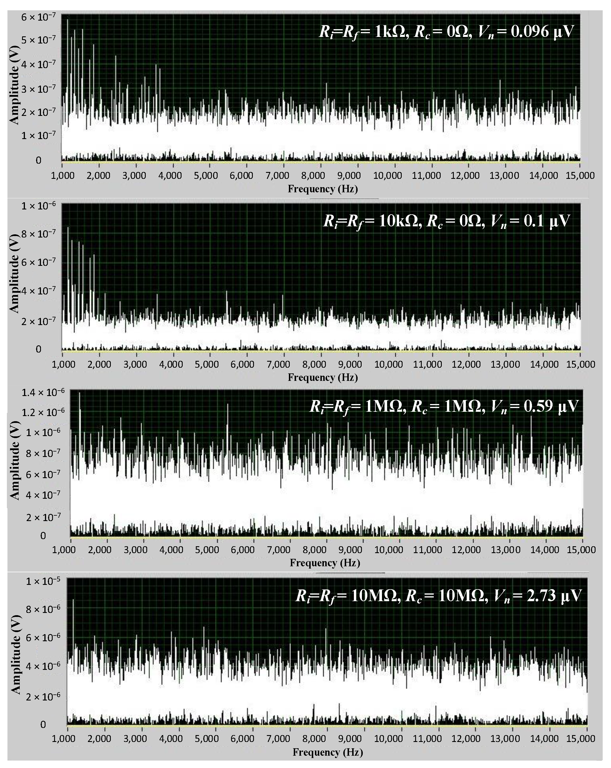
For the inverting amplifier, to study the influence of different resistances (i.e., Ri, Rf, and Rc) on the output noise or SNR of the inverting amplifier, the output noise signal is measured by LabVIEW2015 software when Ri, Rf, and Rc are adjusted, as shown in Figure 7. The models of the operational amplifier and instrumentation amplifier in the tests are AD8676 and AD8421 from Analog Devices, Inc., respectively. In order to facilitate the analysis, Ri is set to equal Rf, so that the gain is 1. Based on the output noise signal, the RMS of the noise can be calculated. Therefore, for different resistance schemes, the RMS of the output noise can be obtained, as listed in Table 1. In this table, the minimum value is 0.096 μV, while the maximum is 2.73 μV. The gap is very large, which indicates that the different parameter setting schemes have a significant impact on the output noise. When Rf and Ri remain constant, the smaller Rc is, the smaller the output noise is. When Ri/Rf and Rc remain constant, the smaller Ri is, and the smaller the output noise is. These test results accord with those of the theoretical analysis above. For other key analog circuits, the conclusions are also similar, so we will not list them one by one. Next, we focus on the noise optimization verification of the whole gyroscope.
Subsequently, the output noises of the gyroscope before and after circuit optimization are measured. The chip selection and parameter setting before and after circuit optimization are depicted in Table 2. The measured results are larger than the theoretical results due to the measurement noise and resolution of the measuring instrument. The detection and control system for an MEMS gyroscope is illustrated in Figure 8. It can be used to realize the system with or without circuit optimization. It is mainly composed of an analog circuit, a digital circuit, and an MEMS gyroscope. The experimental sample is an MEMS gyroscope, namely, model 3#621, fabricated by the National Key Laboratory of Science and Technology on Micro/Nano Fabrication at Peking University. The details about the MEMS gyroscope and the system were given in our previous work [41].
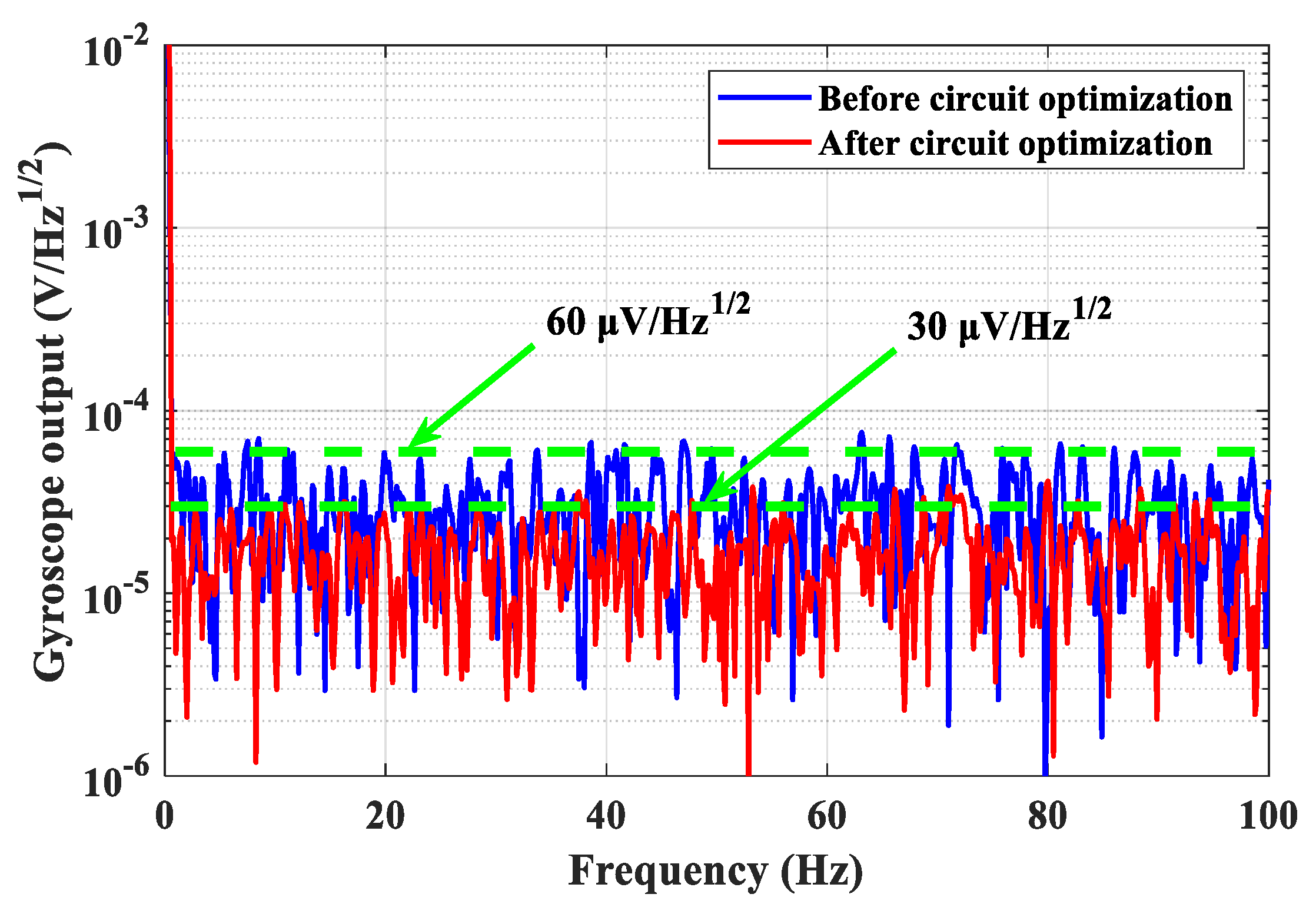
The output noise spectrums of the gyroscope before and after circuit optimization are illustrated in Figure 9. It shows that before circuit optimization, the maximum output noise is about 60 μV/Hz1/2. However, after circuit optimization, it can be significantly reduced to about 30 μV/Hz1/2. In addition, Allan variance is adopted to analyze the noise of the gyroscope, as shown in Figure 10. Before circuit optimization, the bias instability and ARW are 3.8 deg/h and 0.035 deg/h1/2, respectively. However, after circuit optimization, they are improved to 1.38 deg/h and 0.018 deg/h1/2, respectively. Thus, the proposed noise analysis and suppression methods for the detection and control circuits of an MEMS gyroscope are feasible and effective. In addition, it should be noted that due to limitations in amplification or cut-off frequency requirements, the output noise cannot be infinitely reduced and can only be optimized within a limited range.

4. Conclusions

In this paper, an optimized front-end readout circuit and noise suppression methods for an MEMS gyroscope were proposed. To suppress the output noise, an improved readout circuit based on the T-resistor networks was proposed, and the corresponding noise equation was derived in detail. In addition, the noise analysis of the key analog circuits, such as the inverting amplifiers, the first-order low-pass filters, and the first-order high-pass filters, was carried out, and the noise suppression strategy with the optimization of the resistances was proposed. Taking the inverting amplifier as an example, the theoretical derivation was verified by measuring and comparing the output noises of different resistance schemes. In addition, the output noises of the gyroscope before and after circuit optimization were measured. Experimental results demonstrated that the output noise with the circuit optimization was reduced from 60 μV/Hz1/2 to 30 μV/Hz1/2 and the bias instability was reduced from 3.8 deg/h to 1.38 deg/h. In addition, the ARW was significantly improved from 0.035 deg/h1/2 to 0.018 deg/h1/2, which indicates that the noise analysis and suppression methods were effective. This paper mainly analyzed and improved the noises of the key analog circuits. In the future, a detailed analysis of the noises of the critical digital circuits will be conducted. In addition, the individual contribution of each method to the noise reduction and more optimization strategies will be considered to further improve the performances of the MEMS gyroscope.

Author Contributions

C.H.: Methodology, funding acquisition; Y.X.: Investigation, writing—original draft; X.W.: Formal analysis, software; H.W.: Writing—review and editing; L.C.: Project administration; G.Y.: Supervision; Q.H.: Data curation, validation. All authors have read and agreed to the published version of the manuscript.

Funding

This work was partially supported by the National Natural Science Foundation of China (grant no. 62104047), Guangdong Basic and Applied Basic Research Foundation (grant no. 2023A1515010291), Basic and Applied Basic Research Project of Guangzhou Basic Research Program (grant no. 2023A04J1707), and Smart Medical Innovation Technology Center, GDUT (grant no. ZYZX24-037).

Institutional Review Board Statement

Not applicable.

Informed Consent Statement

Not applicable.

Data Availability Statement

The authors do not have permission to share data.

Conflicts of Interest

The authors declare no conflicts of interest.

References

  1. Samatas, G.G.; Pachidis, T.P. Inertial Measurement Units (IMUs) in Mobile Robots over the Last Five Years: A Review. Designs 2022, 6, 17. [Google Scholar] [CrossRef]
  2. Marx, M.; Cuignet, X.; Nessler, S.; De Dorigo, D.; Manoli, Y. An Automatic MEMS Gyroscope Mode Matching Circuit Based on Noise Observation. IEEE Trans. Circuits Syst. II Express Briefs 2019, 66, 743–747. [Google Scholar] [CrossRef]
  3. Rudyk, A.V.; Semenov, A.O.; Kryvinska, N.; Semenova, O.O.; Kvasnikov, V.P.; Safonyk, A.P. Strapdown Inertial Navigation Systems for Positioning Mobile Robots—MEMS Gyroscopes Random Errors Analysis Using Allan Variance Method. Sensors 2020, 20, 4841. [Google Scholar] [CrossRef]
  4. Buffoli, A.; Gadola, M.; Sansa, M.; Langfelder, G. 0.02°/h, 0.004°/√h, 6.3-mA NEMS Gyroscope with Integrated Circuit. IEEE Trans. Instrum. Meas. 2023, 72, 2002108. [Google Scholar] [CrossRef]
  5. Bai, Y.; Wang, X.; Jin, X.; Su, T.; Kong, J.; Zhang, B. Adaptive Filtering for MEMS Gyroscope with Dynamic Noise Model. ISA Transact. 2020, 101, 430–441. [Google Scholar] [CrossRef]
  6. Tan, J.; Kuang, J.; Hu, X.; Cai, X.; Shi, J. The Design of ΔΣ-ADC in MEMS Gyro Interface ASIC. Microelectron. J. 2023, 134, 105696. [Google Scholar] [CrossRef]
  7. Mishra, M.K.; Dubey, V.; Mishra, P.M.; Khan, I. MEMS Technology: A Review. J. Eng. Res. Rep 2019, 4, 1–24. [Google Scholar] [CrossRef]
  8. Tilli, M.; Paulasto-Kröckel, M.; Petzold, M.; Theuss, H.; Motooka, T.; Lindroos, V. Handbook of Silicon Based MEMS Materials and Technologies; Elsevier: Amsterdam, The Netherlands, 2020; ISBN 978-0-12-817787-7. [Google Scholar]
  9. Serri, M.; Saeedi, S. Ultra-Low-Noise TIA Topology for MEMS Gyroscope Readout. AEU Int. J. Electron. Commun. 2020, 118, 153145. [Google Scholar] [CrossRef]
  10. Ying, D.; Hall, D.A. Current Sensing Front-Ends: A Review and Design Guidance. IEEE Sens. J. 2021, 21, 22329–22346. [Google Scholar] [CrossRef]
  11. Harindranath, A.; Arora, M. A Systematic Review of User—Conducted Calibration Methods for MEMS-Based IMUs. Measurement 2024, 225, 114001. [Google Scholar] [CrossRef]
  12. Wang, X.; Zheng, X.; Shen, Y.; Xia, C.; Tong, W.; Jin, Z.; Ma, Z. Noise Analysis and Modeling for a Digital Control Architecture for Lissajous Frequency-Modulated MEMS Gyroscope with Amplitude-Modulated Readout. J. Micromech. Microeng. 2023, 33, 095008. [Google Scholar] [CrossRef]
  13. Liu, X.; Chen, D.; Song, K. A Low-Noise Readout Interface for Silicon MEMS Vibratory Gyroscope. Mod. Phys. Lett. B 2021, 35, 2150069. [Google Scholar] [CrossRef]
  14. Zou, J.; Wei, Q.; Ju, C.; Liao, H.; Gu, H.; Xing, B.; Zhou, B.; Zhang, R. A 0.82 μVrms Ultralow 1/f Noise Bandgap Reference for a MEMS Gyroscope. Microsyst. Nanoeng. 2023, 9, 48. [Google Scholar] [CrossRef]
  15. Zhang, W.; Yin, L.; Wang, Y.; Lv, R.; Zhang, H.; Chen, W.; Liu, X.; Fu, Q. A Low-Noise Interface ASIC for MEMS Disk Resonator Gyroscope. Micromachines 2023, 14, 1256. [Google Scholar] [CrossRef]
  16. Han, S.; Meng, Z.; Omisore, O.; Akinyemi, T.; Yan, Y. Random Error Reduction Algorithms for MEMS Inertial Sensor Accuracy Improvement—A Review. Micromachines 2020, 11, 1021. [Google Scholar] [CrossRef]
  17. Liu, M.; Fan, Q.; Zhou, Y.; Su, Y. A System Phase Noise Model for Frequency-Modulated MEMS Gyroscopes. IEEE Sens. J. 2021, 21, 16124–16133. [Google Scholar] [CrossRef]
  18. Lethander, K.A.; Taylor, C.N. Conservative Estimation of Inertial Sensor Errors Using Allan Variance Data. Navig. J. Inst. Navig. 2023, 70, navi.563. [Google Scholar] [CrossRef]
  19. Pei, H.; Fan, W.; Du, P.; Zhang, K.; Yuan, L.; Quan, W. Markov Noise in Atomic Spin Gyroscopes: Analysis and Suppression Based on Allan Deviation. IEEE Trans. Instrum. Meas. 2023, 72, 7002709. [Google Scholar] [CrossRef]
  20. Catelani, M.; Ciani, L.; Patrizi, G.; Singuaroli, R.; Carratù, M.; Sommella, P.; Pietrosanto, A. Analysis of Noise Contributions in Low-Cost IMUs through Allan’s Variance. In Proceedings of the 2023 IEEE 10th International Workshop on Metrology for AeroSpace (MetroAeroSpace), Milan, Italy, 19–21 June 2023; pp. 258–262. [Google Scholar]
  21. Lin, J.; Pham, L.; Tao, R.; Gutmann, A.; Guo, S.; Cywar, A.; Spirer, A.; Mansson, J.; Nguyen, K. A Low-Power, Wide-Bandwidth, Three-Axis MEMS Accelerometer ASIC Using Beyond-Resonant-Frequency Sensing. IEEE J. Solid-State Circuits 2024, 59, 774–783. [Google Scholar] [CrossRef]
  22. Zhong, L.; Liu, S.; Xu, D.; Zhu, Z. A 63 Μg/√Hz Noise Floor and 14 pJ Power Efficiency Open-Loop MEMS Capacitive Accelerometer Using Closed-Loop Hybrid Dynamic Amplifier. IEEE Trans. Circuits Syst. I Regul. Pap. 2023, 70, 1531–1541. [Google Scholar] [CrossRef]
  23. Bu, F.; Fan, B.; Xu, D.; Guo, S.; Zhao, H. Bandwidth and Noise Analysis of High-Q MEMS Gyroscope under Force Rebalance Closed-Loop Control. J. Micromech. Microeng. 2021, 31, 065002. [Google Scholar] [CrossRef]
  24. Liu, M.; Fan, Q.; Zhao, J.; Su, Y. A Phase Compensation Method for MEMS Quadruple Mass Gyroscope in Zero Bias Drift. IEEE Sens. J. 2021, 21, 3087–3096. [Google Scholar] [CrossRef]
  25. Bu, F.; Wang, X.; Fan, B.; Guo, S.; Xu, D.; Xu, X.; Zhao, H. Noise Model Considering Electrical Feed-through under Force Rebalance Closed-Loop Detection of MEMS Gyroscope. J. Micromech. Microeng. 2020, 30, 055007. [Google Scholar] [CrossRef]
  26. Xia, G.; Zhao, Y.; Shi, Q.; Huang, J.; Qiu, A. A Novel Frequency Readout Method and Circuit for Navigation-Grade Vibrating Beam Accelerometers. IEEE Sens. J. 2023, 23, 21363–21373. [Google Scholar] [CrossRef]
  27. Chen, Y.; Zhu, L.; Cao, Y.; Wang, W.; Huang, H.; He, Y.; Ma, X.; Li, Z. Suppression of Self-Noise and Environmental Disturbances by Fusion in Fiber-Optic Gyroscopes for Precision Measurement. IEEE Sens. J. 2023, 23, 14084–14094. [Google Scholar] [CrossRef]
  28. Zhang, H.; Chen, W.; Yin, L.; Fu, Q. Analysis and Design of a Fourth-Order ΣΔ ADC for MEMS Digital Gyroscope Sensors. Microelectron. J. 2023, 141, 105953. [Google Scholar] [CrossRef]
  29. Pawase, R.; Futane, N.P. Angular Rate Error Compensation of MEMS Based Gyroscope Using Artificial Neural Network. In Proceedings of the 2015 International Conference on Pervasive Computing (ICPC), Pune, India, 8–10 January 2015; pp. 1–4. [Google Scholar]
  30. Zhang, Y.; Yang, T. Modeling and Compensation of MEMS Gyroscope Output Data Based on Support Vector Machine. Measurement 2012, 45, 922–926. [Google Scholar] [CrossRef]
  31. Liu, N.; Su, Z.; Li, Q.; Zhao, H.; Qi, W. A Combined CKF-PSR Method for Random Noise Compensation of Vibratory Gyroscopes. J. Ind. Inf. Integr. 2022, 25, 100241. [Google Scholar] [CrossRef]
  32. Abbasi, J.; Hashemi, M.; Alasty, A. A Memory-Based Filter for Long-Term Error De-Noising of MEMS-Gyros. IEEE Trans. Instrum. Meas. 2022, 71, 7503308. [Google Scholar] [CrossRef]
  33. Cao, H. Temperature Influence on Silicon-Based MEMS Gyroscope and Suppression Method. In Dual-Mass Linear Vibration Silicon-Based MEMS Gyroscope; Cao, H., Ed.; Springer Nature: Singapore, 2023; pp. 167–198. ISBN 978-981-19924-7-6. [Google Scholar]
  34. Wang, Y.; Cao, R.; Li, C.; Dean, R.N. Concepts, Roadmaps and Challenges of Ovenized MEMS Gyroscopes: A Review. IEEE Sens. J. 2021, 21, 92–119. [Google Scholar] [CrossRef]
  35. Jiancheng, F.; Jianli, L. Integrated Model and Compensation of Thermal Errors of Silicon Microelectromechanical Gyroscope. IEEE Trans. Instrum. Meas. 2009, 58, 2923–2930. [Google Scholar] [CrossRef]
  36. Zhao, Y.; Shi, Q.; Xia, G.; Qiu, A. Low-Noise Quality Factor Tuning in Nondegenerate MEMS Gyroscope Without Dedicated Tuning Electrode. IEEE Trans. Ind. Electron. 2024, 71, 4230–4240. [Google Scholar] [CrossRef]
  37. Zhang, H.; Chen, W.; Yin, L.; Fu, Q. Design of MEMS Gyroscope Interface ASIC with On-Chip Temperature Compensation. Measurement 2023, 220, 113331. [Google Scholar] [CrossRef]
  38. Cetin, H.; Yaralioglu, G. Noise Analysis of Mode Matched Vibratory Gyroscopes. Microsyst Technol 2023, 29, 35–47. [Google Scholar] [CrossRef]
  39. Li, C.; Sun, Z.; Zhou, L.; Zheng, X.; Guo, X.; Huang, X.; Yang, B. Microseismic Observation Enabled by High-Sensitivity Micromechanical Interferometers. IEEE Trans. Ind. Electron. 2024, 71, 5349–5359. [Google Scholar] [CrossRef]
  40. Ren, X.; Zhou, X.; Yu, S.; Wu, X.; Xiao, D. Frequency-Modulated MEMS Gyroscopes: A Review. IEEE Sens. J. 2021, 21, 26426–26446. [Google Scholar] [CrossRef]
  41. He, C.; Zhang, J.; Zhao, Q.; Huang, Q.; Yang, Z.; Zhang, D.; Yan, G. An Electrical-Coupling-Suppressing MEMS Gyroscope with Feed-Forward Coupling Compensation and Scalable Fuzzy Control. Sci. China Inf. Sci. 2017, 60, 042402. [Google Scholar] [CrossRef]
Figure 1. Schematic of the front-end readout circuit with feed-forward coupling compensation control.
Sensors 24 06283 g001
Figure 2. Noise model for a front-end readout circuit with feed-forward coupling compensation control.
Sensors 24 06283 g002
Figure 3. Schematic of an improved front-end readout circuit based on T-resistor networks.
Sensors 24 06283 g003
Figure 4. Noise analysis for an improved front-end readout circuit based on T-resistor networks.
Sensors 24 06283 g004
Figure 5. (a) Schematic of the inverting amplifier; (b) noise analysis for the inverting amplifier.
Sensors 24 06283 g005
Figure 6. (a) Noise analysis for the first-order low-pass filter; (b) noise analysis for the first-order high-pass filter.
Sensors 24 06283 g006
Figure 7. The output noise signal is measured by LabVIEW software when Ri, Rf, and Rc are adjusted.
Sensors 24 06283 g007
Figure 8. The detection and control system for an MEMS gyroscope.
Sensors 24 06283 g008
Figure 9. The output noise spectrums of the gyroscope before and after circuit optimization.
Sensors 24 06283 g009
Figure 10. Allan variance curves of the gyroscope before and after circuit optimization.
Sensors 24 06283 g010
Table 1. The noise test and theoretical results of different resistance schemes.
TestRi (Ω)Rf (Ω)Rc (Ω)Test Result
Vn (μV)
11 k1 k00.096
21 k1 k10 M3
310 k10 k00.1
410 k10 k10 k0.11
5100 k100 k00.13
6100 k100 k100 k0.19
71 M1 M00.35
81 M1 M1 M0.59
910 M10 M01.98
1010 M10 M10 M2.73
Table 2. The chip selection and parameter setting before and after circuit optimization.
TypeBefore Circuit OptimizationAfter Circuit Optimization
Chip selectionOP2177, AD8221AD8676, AD8421
Transimpedance amplifierWithout T-resistor networks
Rf = 1 MΩ, Cf = 1 pF
With T-resistor networks
R11 = 100 kΩ, R12 = 1 kΩ, R13 = 110 Ω, Cf = 1 pF
Inverting amplifierRf = 100 kΩ, Ri = 100 kΩ, Rc = 100 kΩRf = 1 kΩ, Ri = 1 kΩ, Rc = 0 Ω
LPFRf = 200 kΩ, Ri = 200 kΩ, Ci = 1 pF, Rc = 100 kΩRf = 2 kΩ, Ri = 2 kΩ, Ci = 100 pF, Rc = 0 Ω
HPFRf = 200 kΩ, Ri = 200 kΩ, Ci = 0.01 μF, Rc = 100 kΩRf = 2 kΩ, Ri = 2 kΩ, Ci = 1 μF, Rc = 0 Ω
Disclaimer/Publisher’s Note: The statements, opinions and data contained in all publications are solely those of the individual author(s) and contributor(s) and not of MDPI and/or the editor(s). MDPI and/or the editor(s) disclaim responsibility for any injury to people or property resulting from any ideas, methods, instructions or products referred to in the content.