
A Piezoresistive-Sensor Nonlinearity Correction on-Chip Method with Highly Robust Class-AB Driving Capability


Abstract
1. Introduction
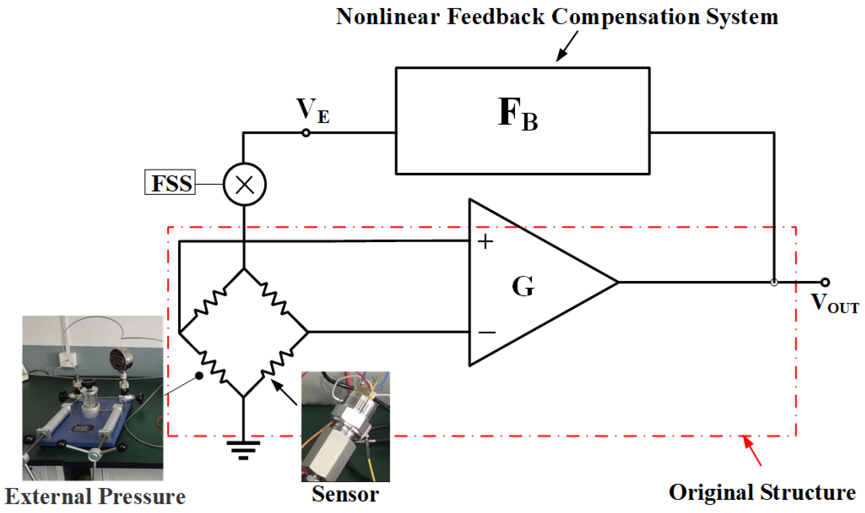
2. Proposed Nonlinear Correction Structure of Piezoresistive Sensor
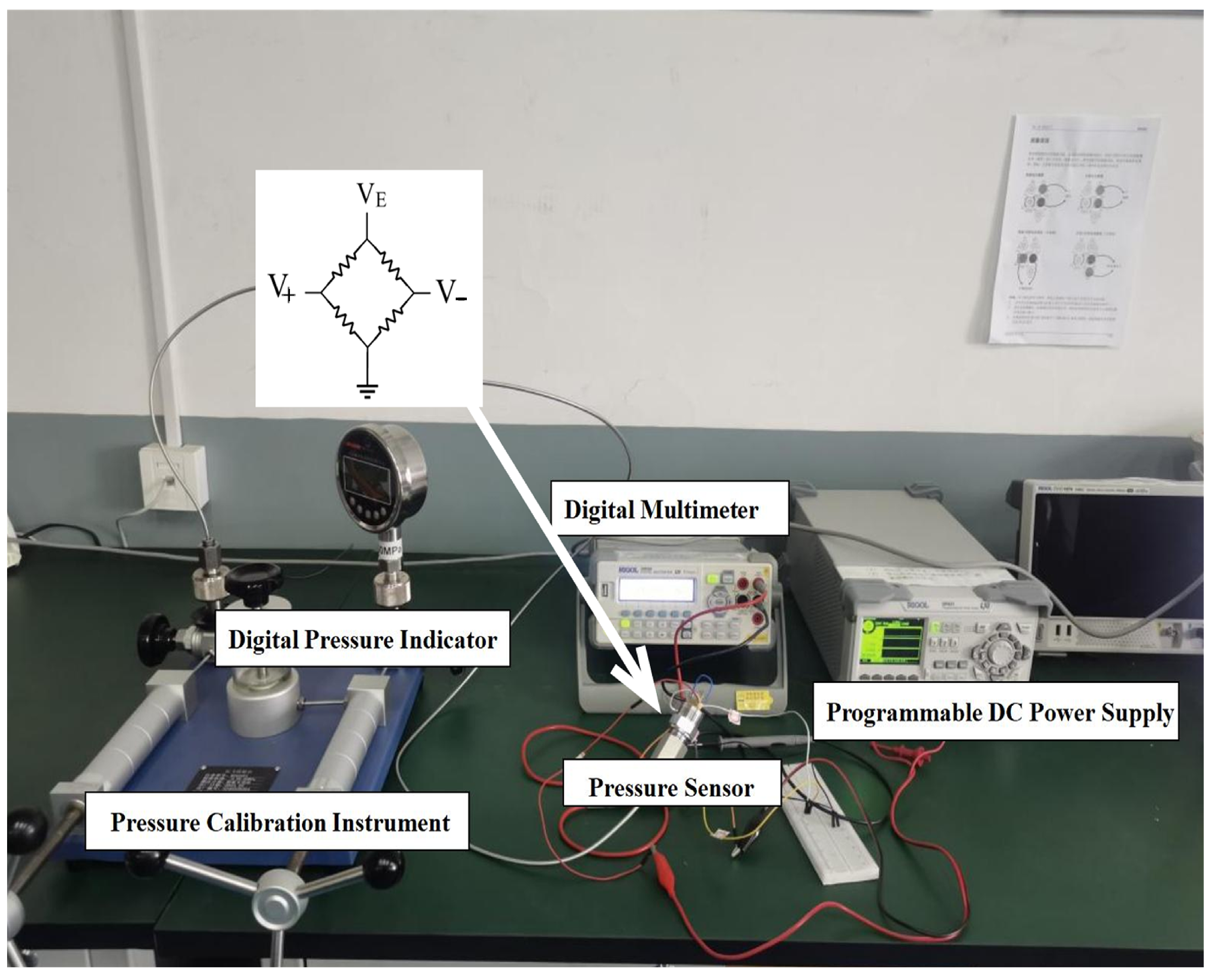
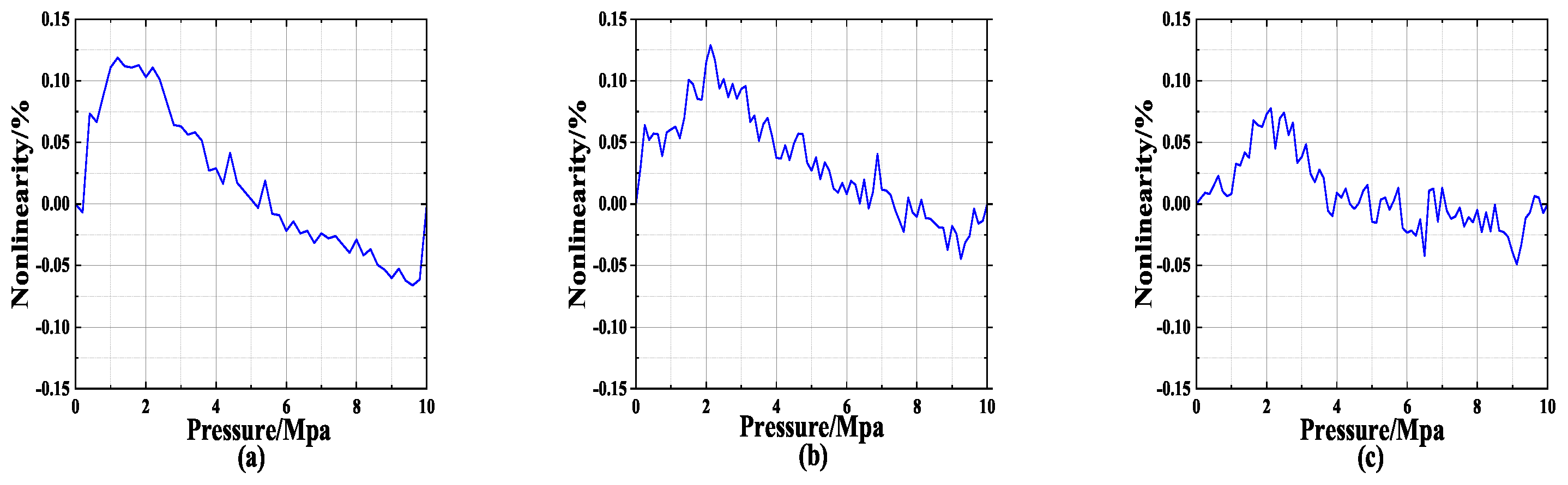
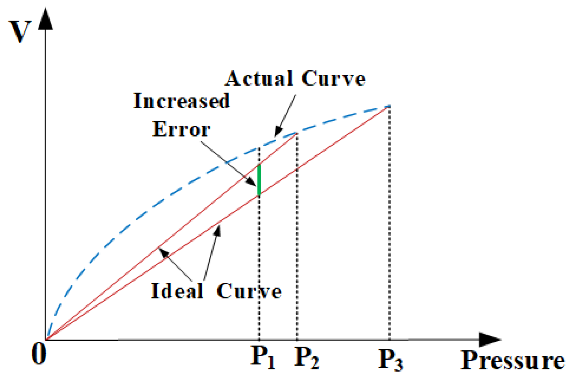
2.1. Silicon Voltage Detection Experiment
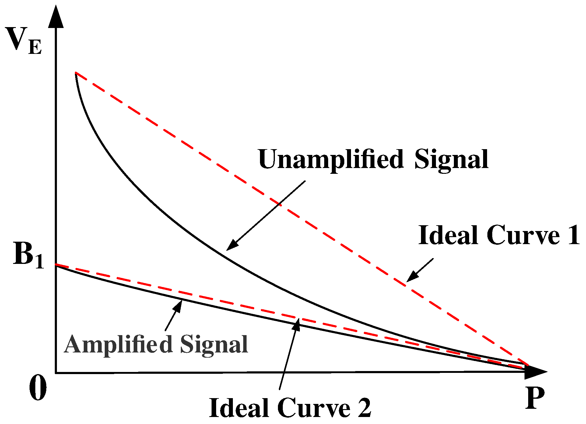
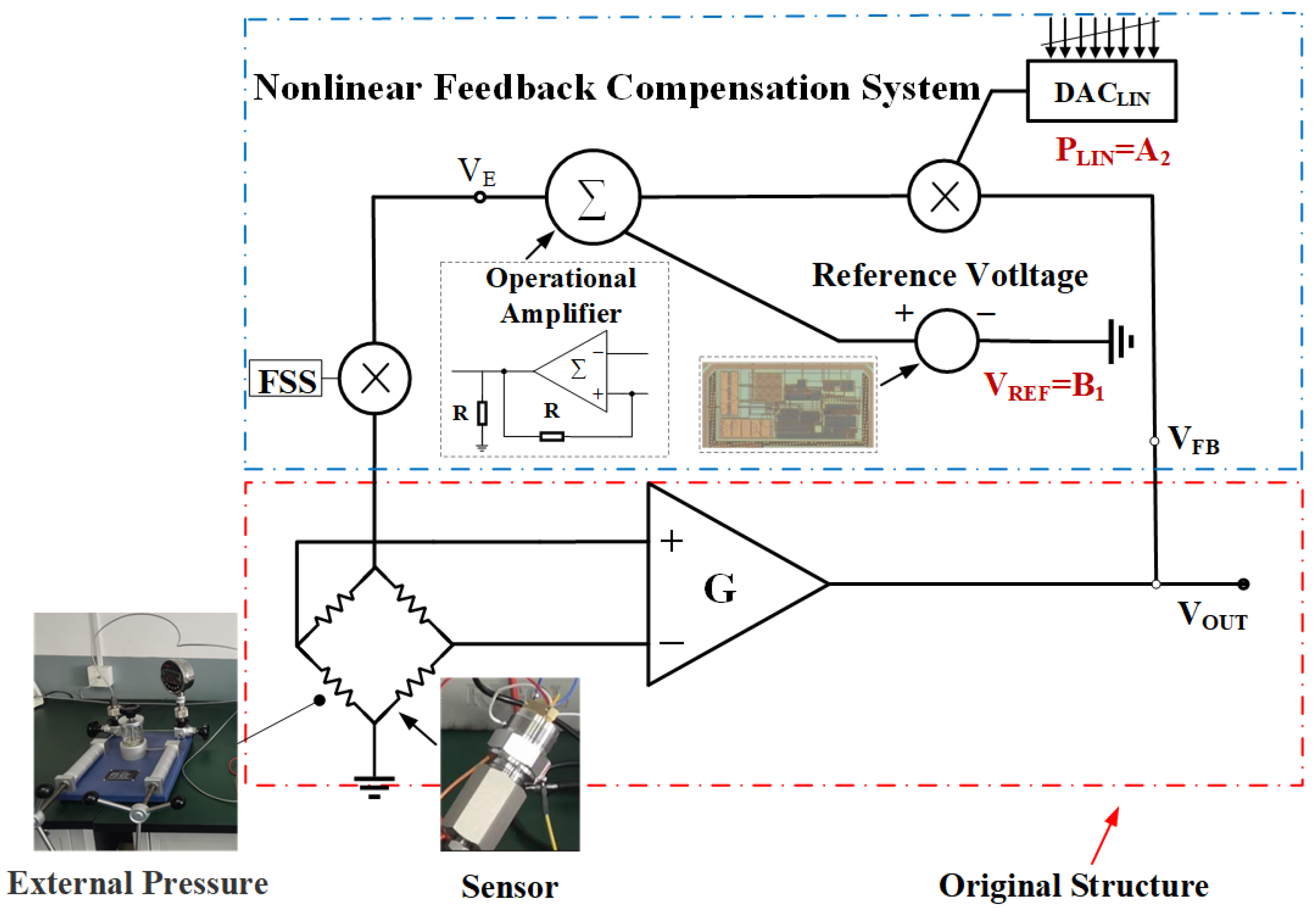
2.2. Proposed Nonlinear Correction Structure of Piezoresistive Sensor
2.3. Model Establishment of
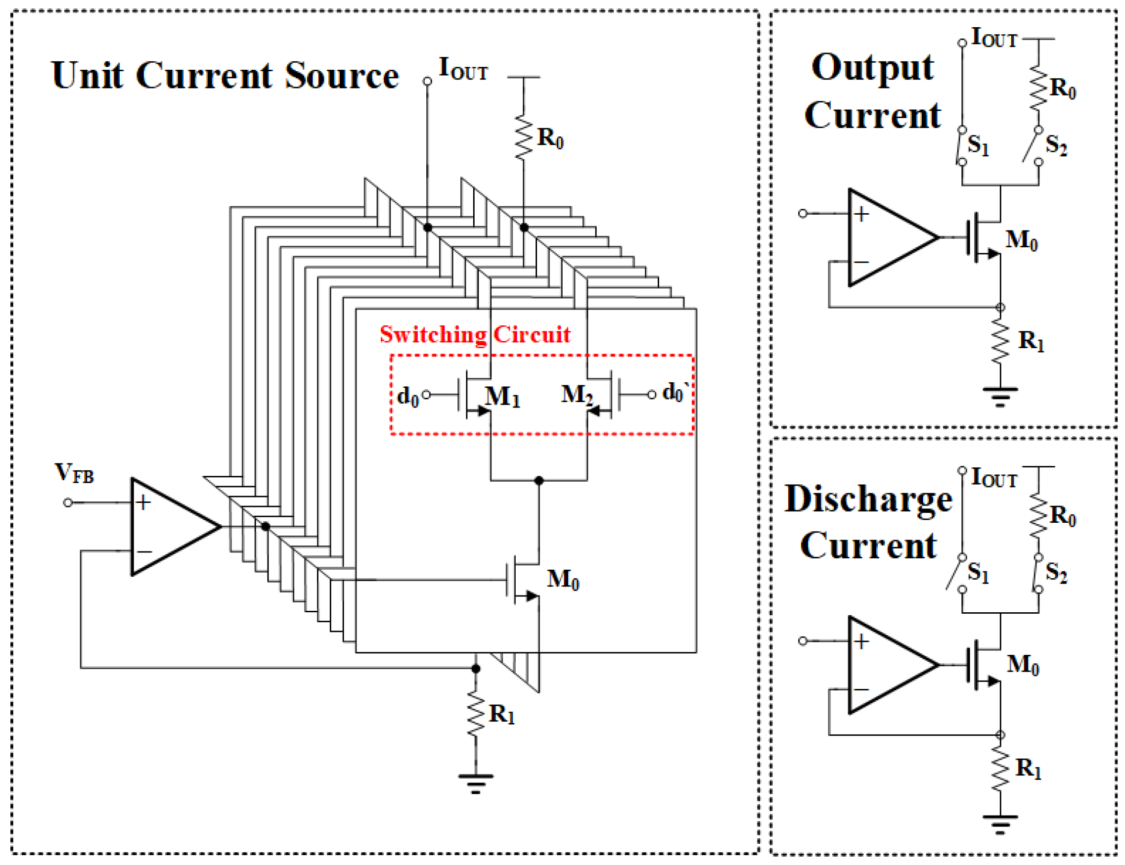
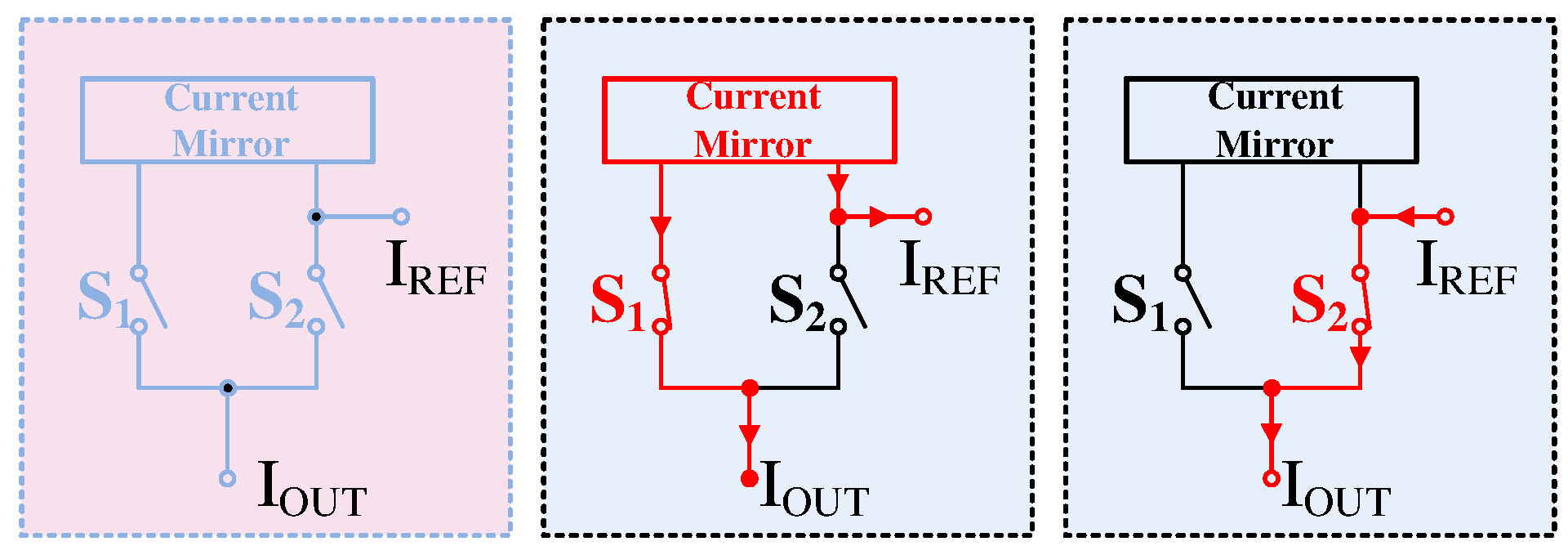
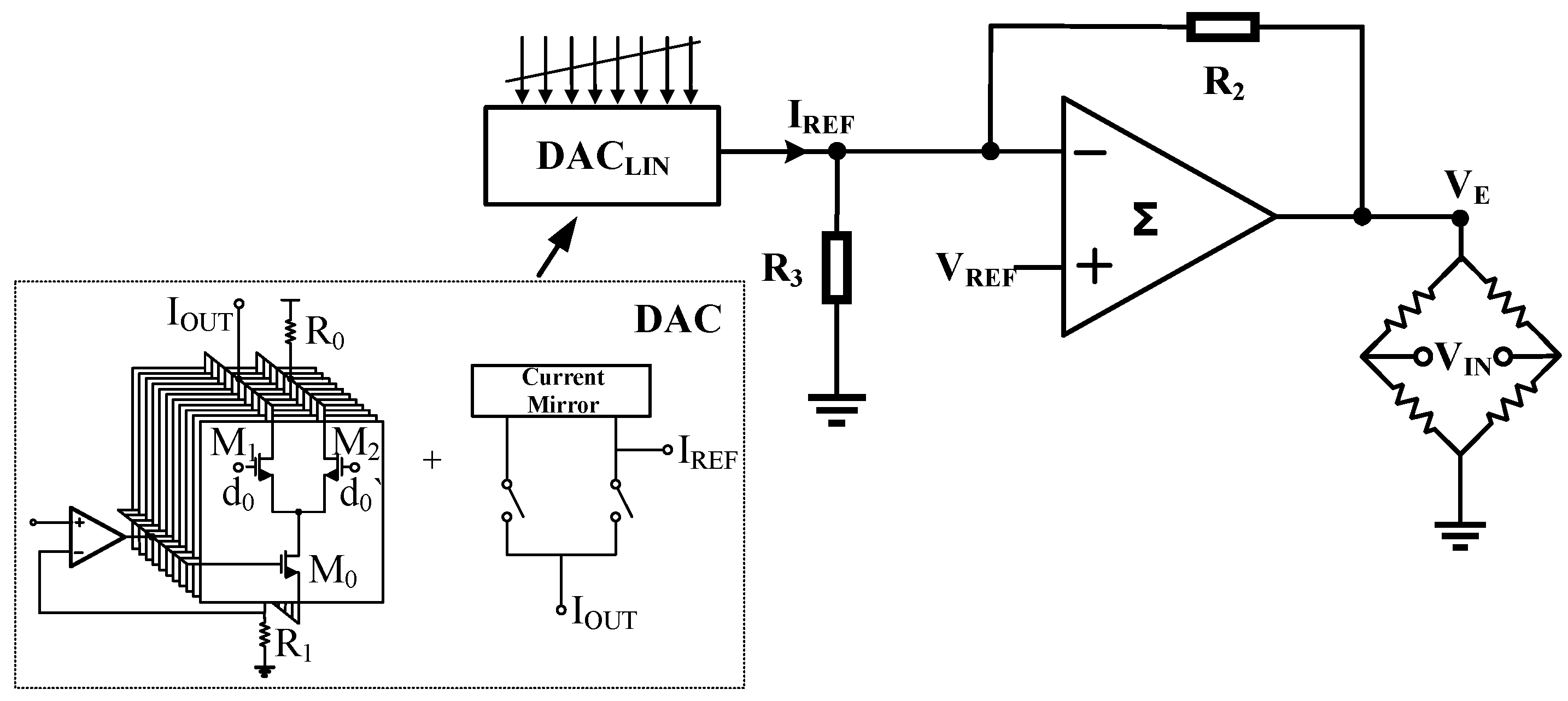
3. Design of Current Steering DAC for Nonlinear Calibration
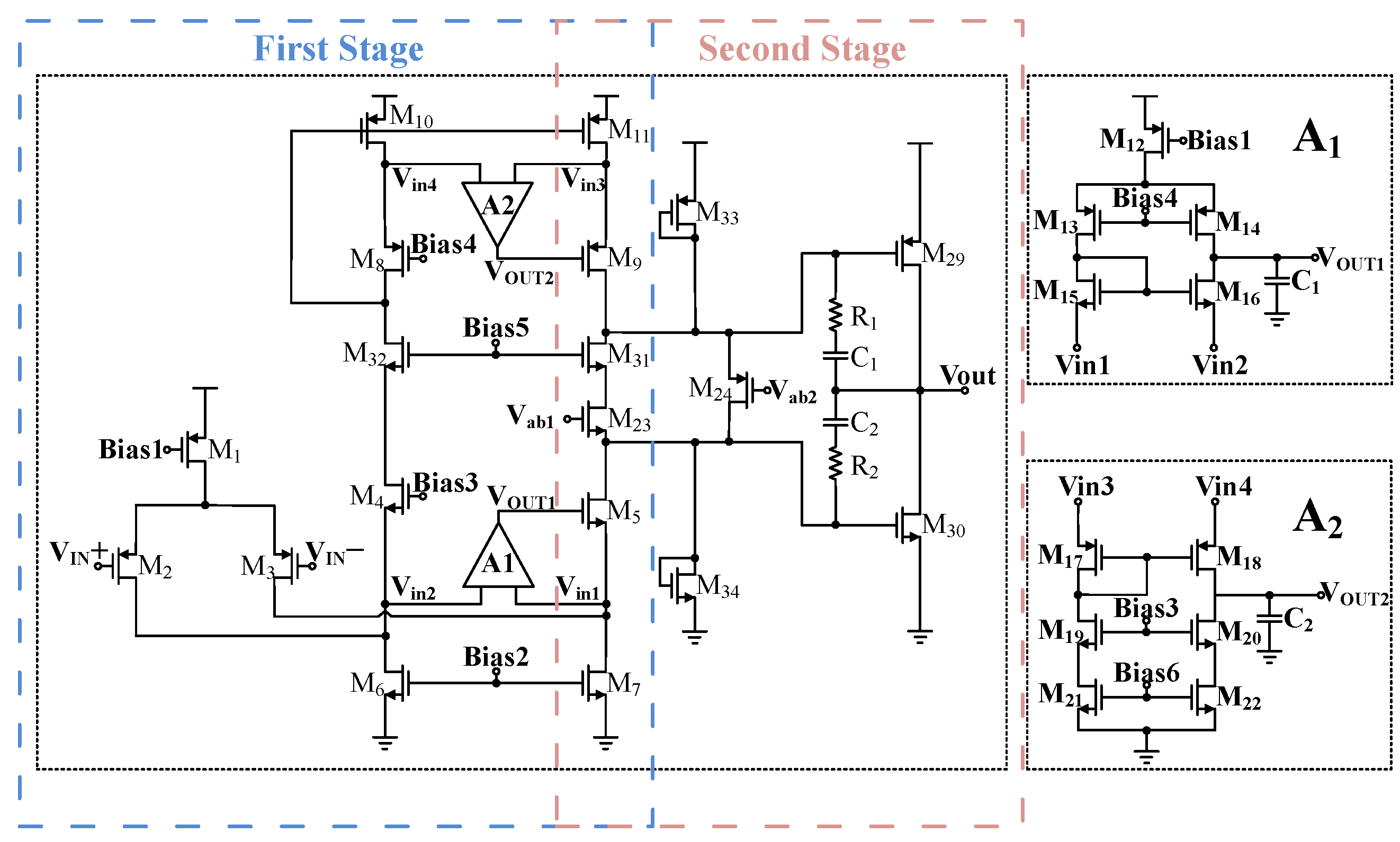
4. Design of the Two-Stage Operational Amplifier with Class-AB Output Stage
4.1. Functional Structure Design of the Operational Amplifier
4.2. Design of the First-Stage Operational Amplifier: Folded Cascode Operational Amplifier Structure
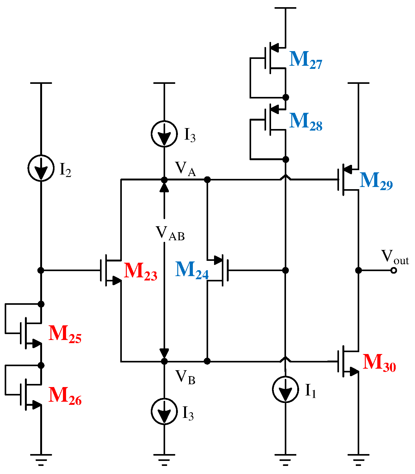
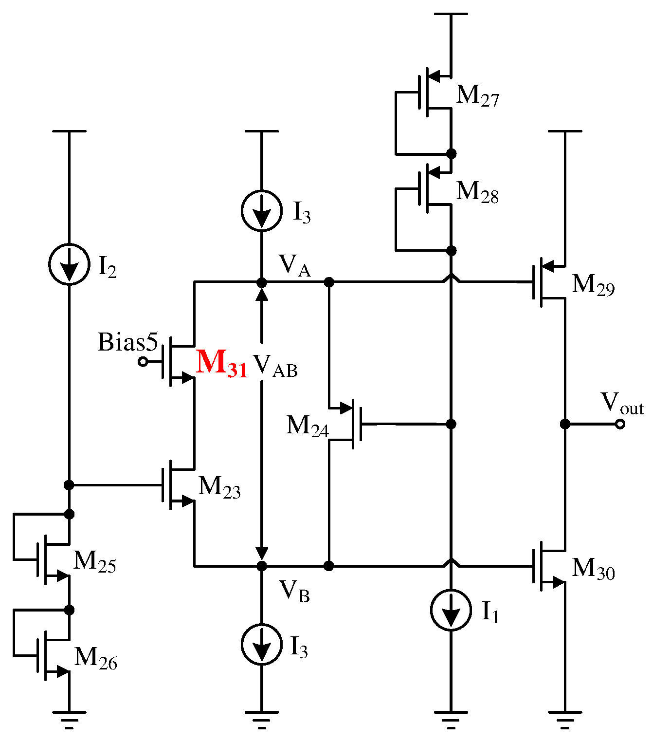
4.3. Design of the Second Stage Operational Amplifier: Improved Class-AB Output Stage Circuit Structure
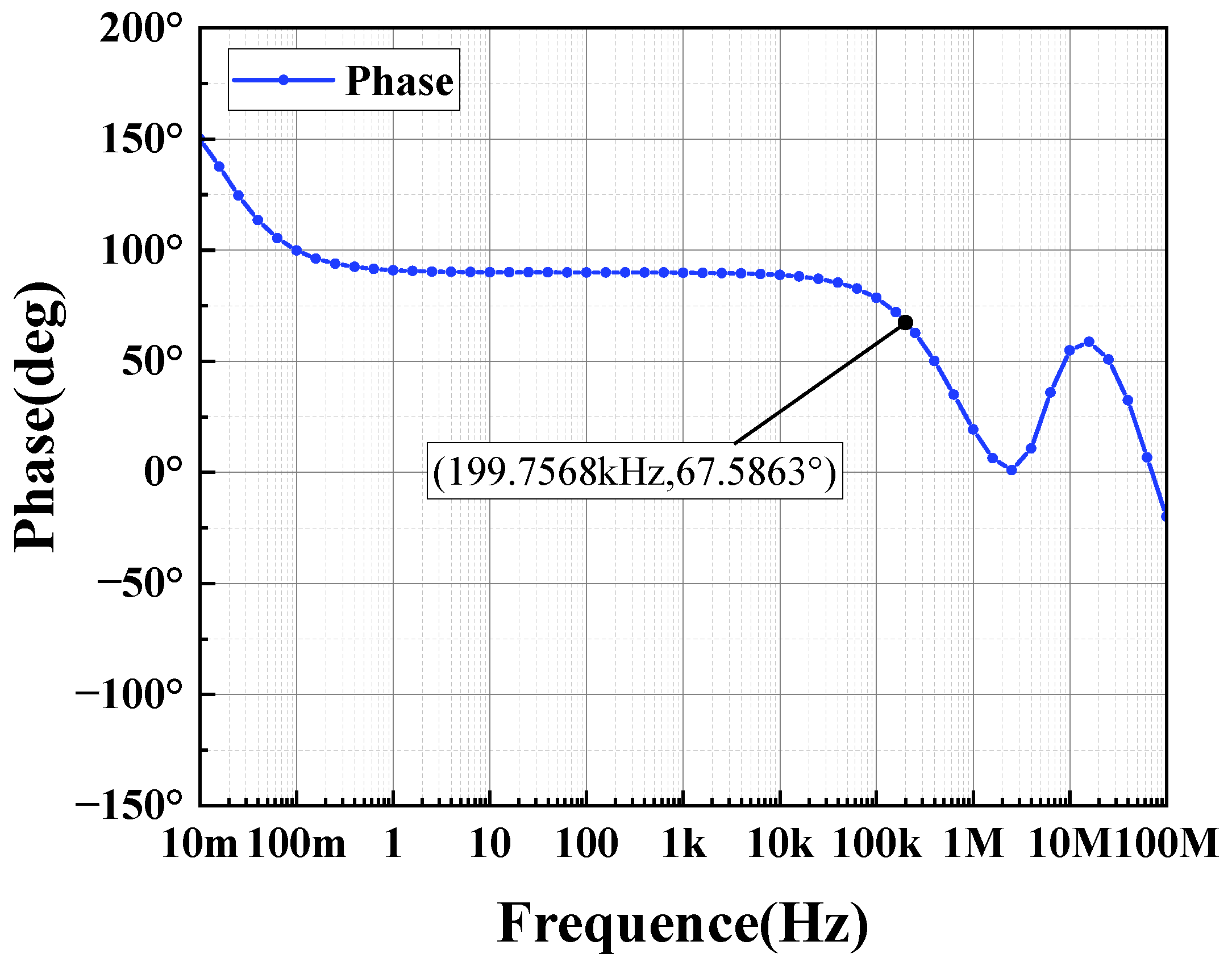
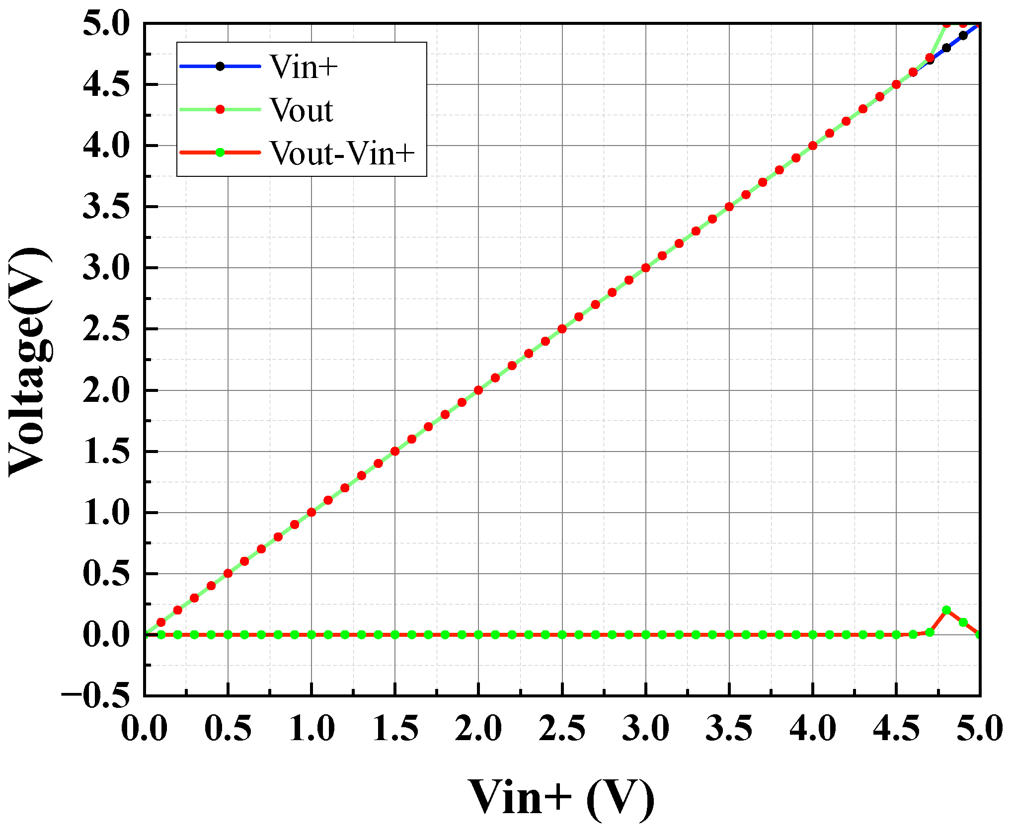
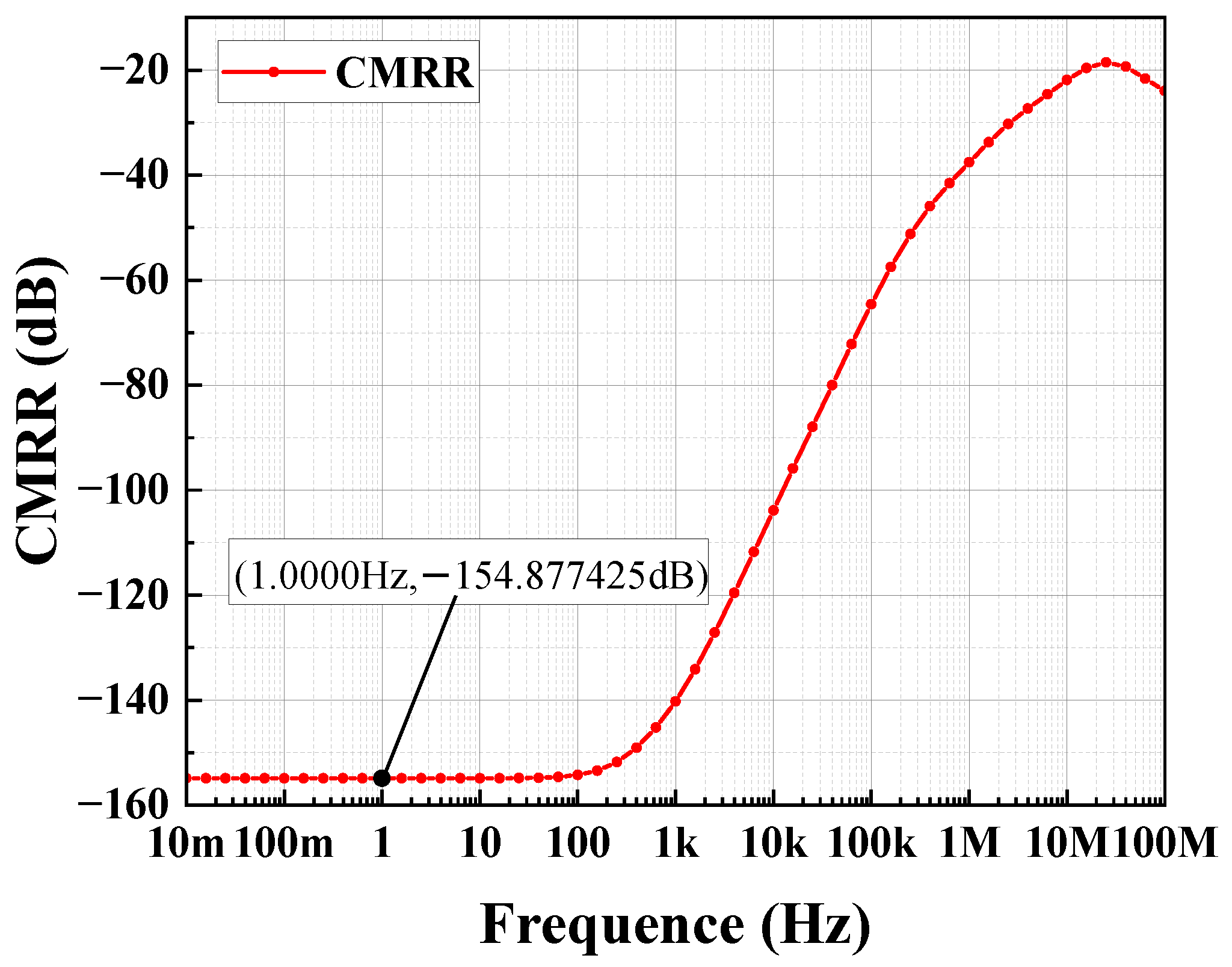
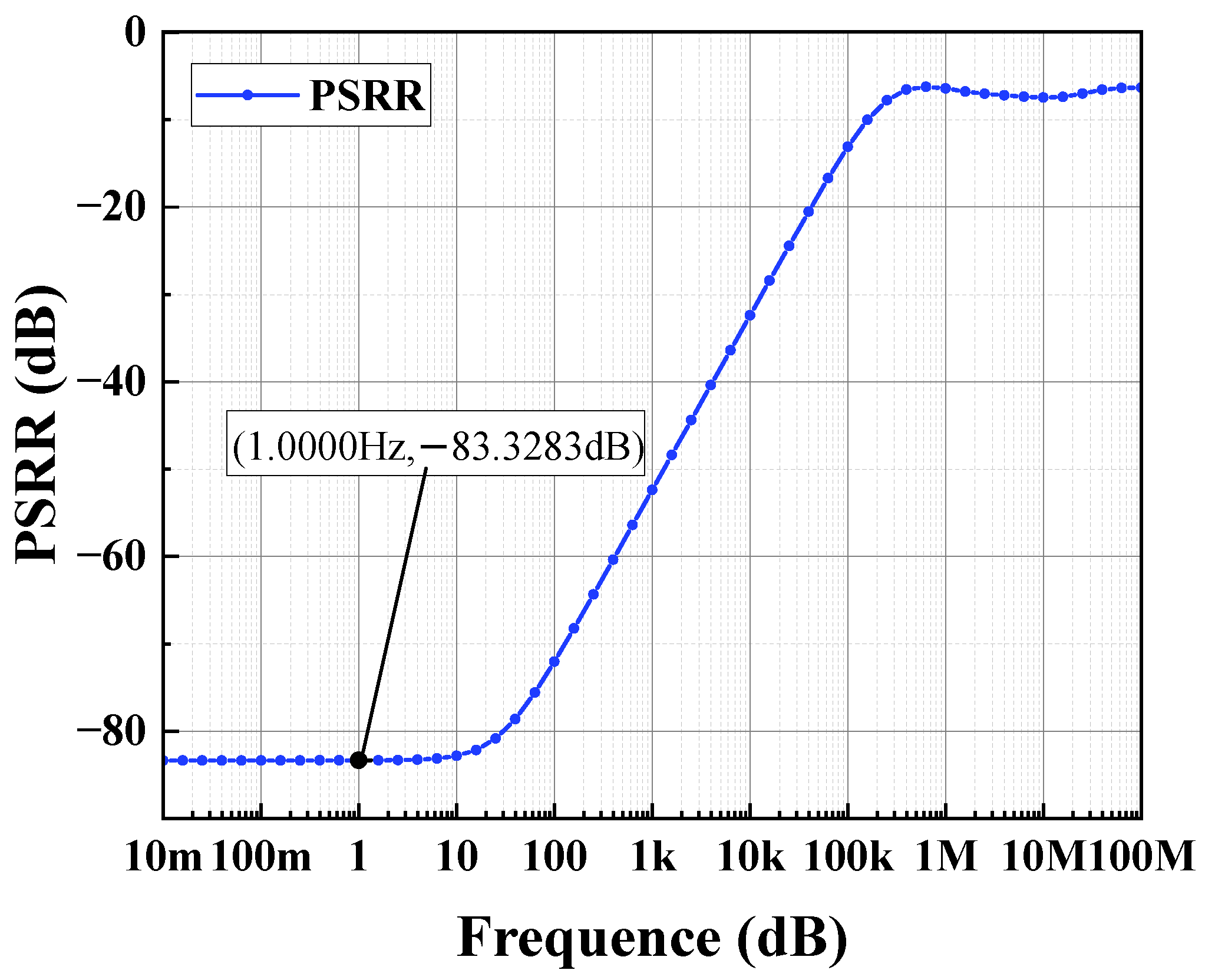
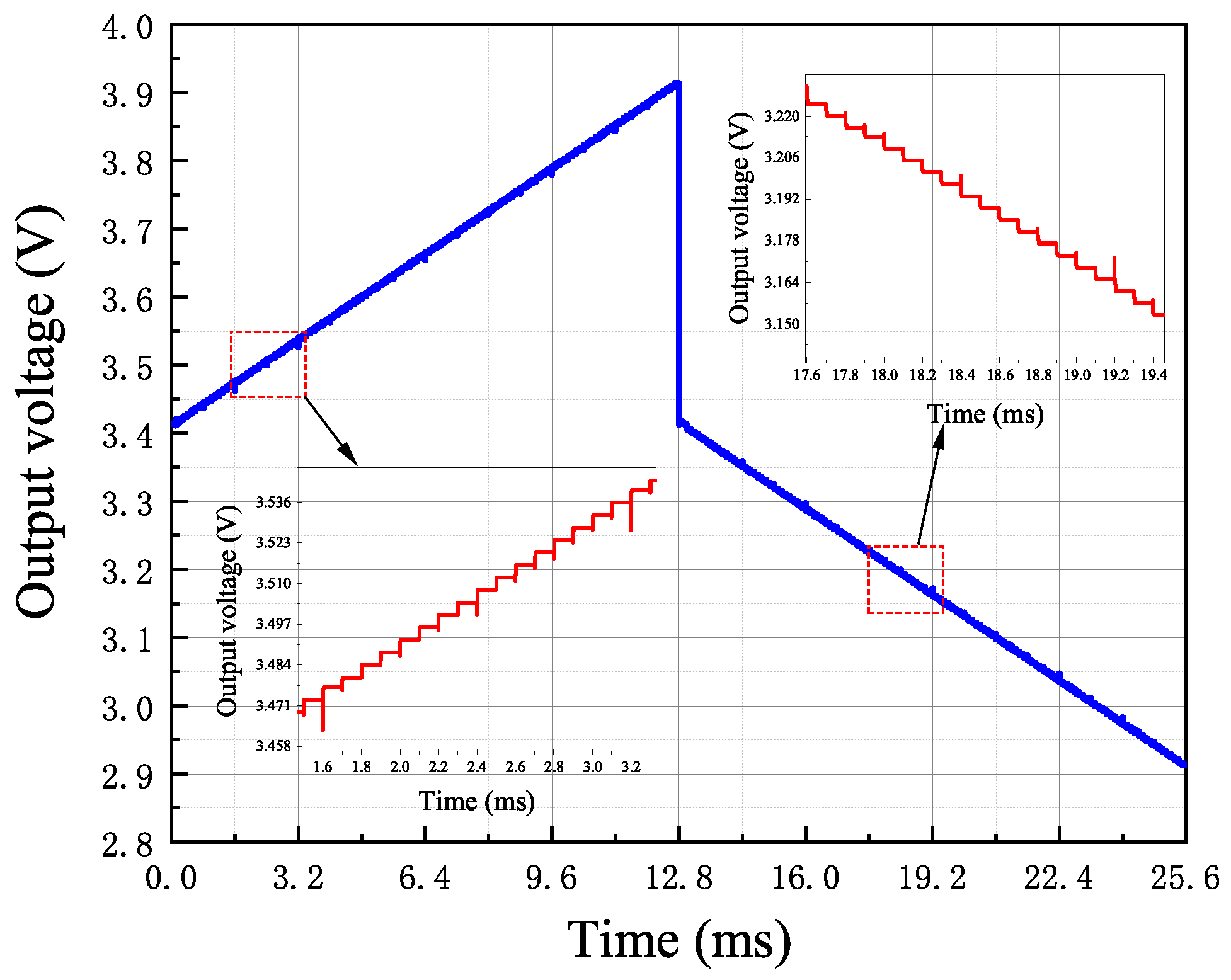
4.4. Post-Simulation Results
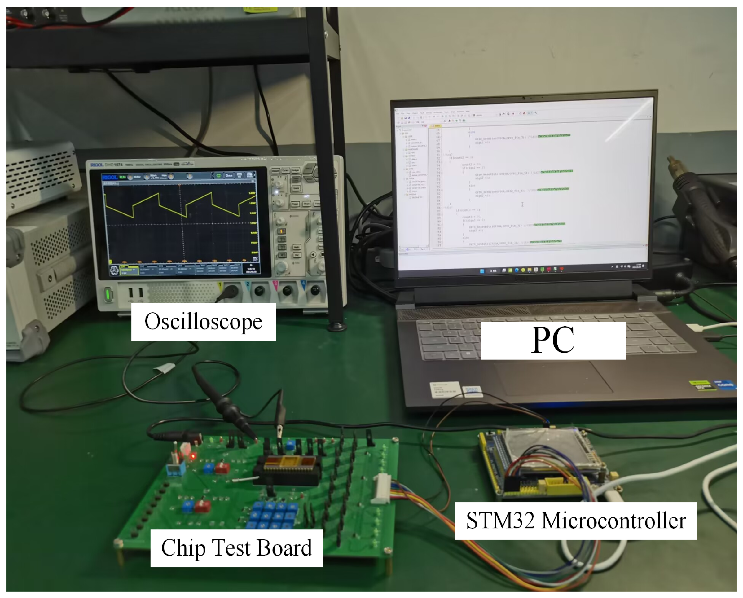
5. Test Results and Discussion
5.1. Measurements of the Current Steering DAC
5.2. DAC Test Experiments
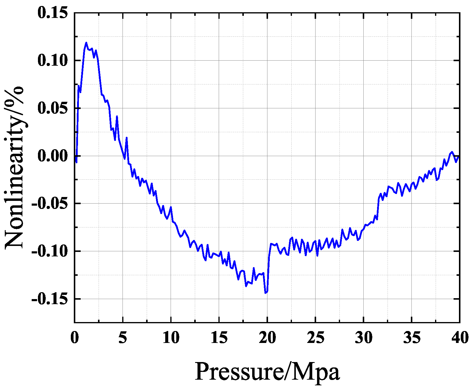
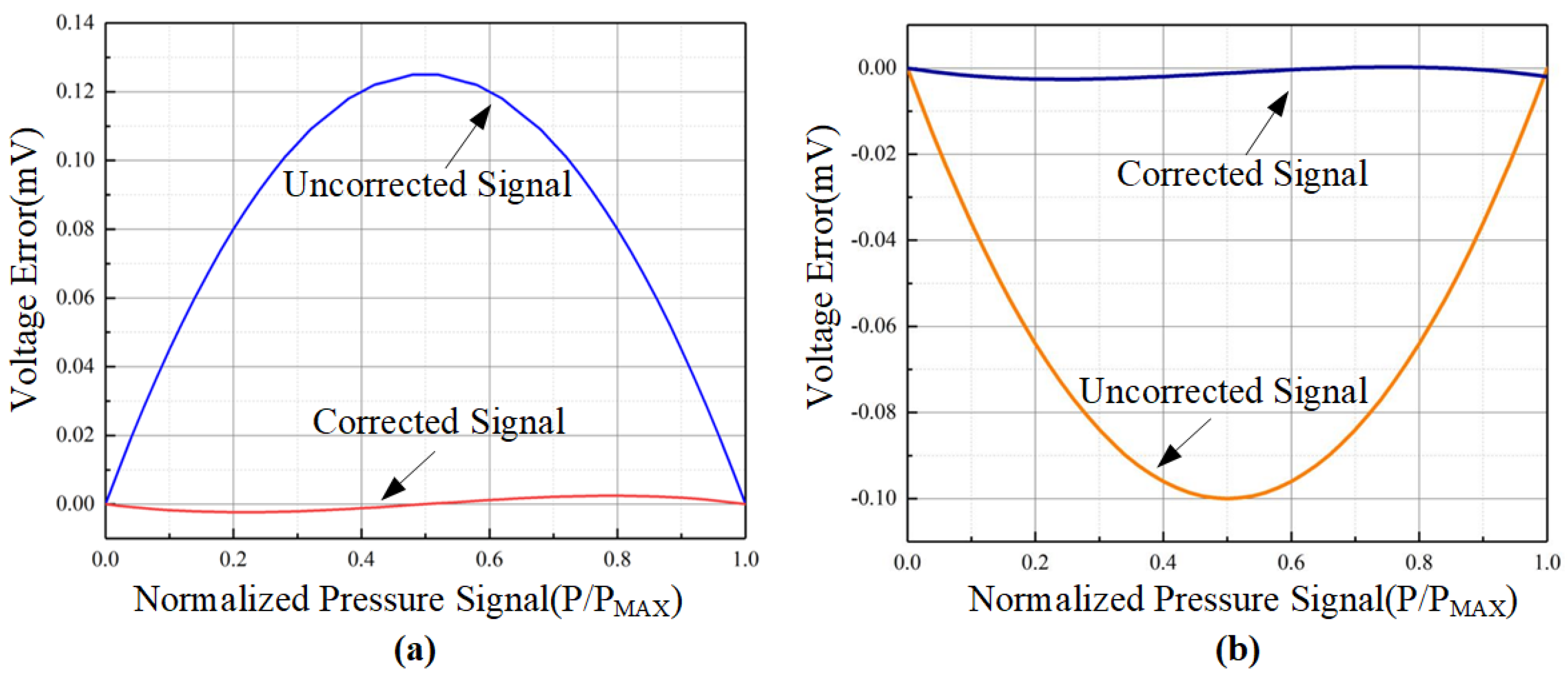
5.3. Simulation Test Results of the Nonlinear Calibration Function
6. Conclusions
Author Contributions
Funding
Institutional Review Board Statement
Informed Consent Statement
Data Availability Statement
Conflicts of Interest
References
- Chen, J.; Liu, Y.; Li, S.; Lin, L.; Li, Y.; Huang, W.; Guo, J. Ferroelectric-controlled graphene plasmonic surfaces for all-optical neuromorphic vision. Sci. China Technol. Sci. 2024, 76, 765–773. [Google Scholar] [CrossRef]
- Baeumer, C.; Saldana-Greco, D.; Martirez, J.M.P.; Rappe, A.M.; Shim, M.; Martin, L.W. Ferroelectrically driven spatial carrier density modulation in graphene. Nat. Commun. 2015, 6, 6136. [Google Scholar] [CrossRef] [PubMed]
- Guo, J.; Gu, S.; Lin, L.; Liu, Y.; Cai, J.; Cai, H.; Tian, Y.; Zhang, Y.; Zhang, Q.; Liu, Z.; et al. Type-printable photodetector arrays for multichannel meta-infrared imaging. Nat. Commun. 2024, 15, 5193. [Google Scholar] [CrossRef] [PubMed]
- Martin, L.; Rappe, A. Thin-film ferroelectric materials and their applications. Nat. Rev. Mater. 2016, 2, 16087. [Google Scholar] [CrossRef]
- Yan, C.; Wang, J.; Kang, W.; Cui, M.; Wang, X.; Foo, C.Y.; Chee, K.J.; Lee, P.S. Highly stretchable piezoresistive graphene–nanocellulose nanopaper for strain sensors. Adv. Mater. 2014, 26, 2022–2027. [Google Scholar] [CrossRef] [PubMed]
- Ramalingame, R.; Barioul, R.; Li, X.; Sanseverino, G.; Krumm, D.; Odenwald, S.; Kanoun, O. Wearable Smart Band for American Sign Language Recognition With Polymer Carbon Nanocomposite-Based Pressure Sensors. IEEE Sens. Lett. 2021, 5, 6001204. [Google Scholar] [CrossRef]
- Hsu, Y.P.; Liu, Z.; Hella, M. A 10 W–74.6 dB THD Arterial Pulse Waveform Sensing System with Automatic Bridge-Offset Calibration and Super Class-AB Output Stage. In Proceedings of the 2019 IEEE Asian Solid-State Circuits Conference (A-SSCC), Macao, 4–6 November 2019. [Google Scholar]
- Pervez, K.; Aman, W.; Rahman, M.M.U.; Nawaz, M.W.; Abbasi, Q.H. Hand-Breathe: Noncontact Monitoring of Breathing Abnormalities From Hand Palm. IEEE Sens. J. 2023, 23, 25136–25143. [Google Scholar] [CrossRef]
- Park, Y.; Gwon, N.H.; Seong, W.K.; Kim, W. Heater-Integrated Flexible Piezoresistive Pressure Sensor Array for Smart-Car Seats. IEEE Sens. J. 2024, 24, 1255–1263. [Google Scholar] [CrossRef]
- Kumar, V.N.; Narayana, K.V.L.; Bhujangarao, A.; Sankar, S. Development of an ANN-Based Linearization Technique for the VCO Thermistor Circuit. IEEE Sens. J. 2015, 15, 886–894. [Google Scholar] [CrossRef]
- Kabanov, A.A.; Esimkhanova, A.M.; Nikonova, G.V.; Sirotenko, N.Y.; Soloviev, V.V. A software-hardware unit for studying the output characteristic of MEMS pressure sensors and its linearization. J. Phys. 2021, 1901, 12009–12018. [Google Scholar] [CrossRef]
- Nishigaki, T.; Hayashi, T.; Takahashi, Y.; Yoshida, K.; Hitomi, Y.; Mizuno-Matsumoto, Y. In vitro evaluation of a new heating system of extracorporeal membrane oxygenation (ECMO) system for children. In Proceedings of the 2010 World Automation Congress, Kobe, Japan, 19–23 September 2010. [Google Scholar]
- Alvarez, J.T.; Gerez, L.F.; Araromi, O.A.; Hunter, J.G.; Choe, D.K.; Payne, C.J.; Wood, R.J.; Walsh, C.J. Towards Soft Wearable Strain Sensors for Muscle Activity Monitoring. IEEE Trans. Neural Syst. Rehabil. 2022, 30, 2198–2206. [Google Scholar] [CrossRef] [PubMed]
- Alvarez, J.T.; Gerez, L.F.; Araromi, O.A.; Hunter, J.G.; Choe, D.K.; Payne, C.J.; Wood, R.J.; Walsh, C.J. Neckband-Based Continuous Blood Pressure Monitoring Device with Offset-Tolerant ROIC. IEEE Access 2022, 10, 17300–17309. [Google Scholar]
- Li, T.; Shang, H.; Wang, B.; Mao, C.; Wang, W. High-Pressure Sensor with High Sensitivity and High Accuracy for Full Ocean Depth Measurements. IEEE Sens. J. 2022, 22, 3994–4003. [Google Scholar] [CrossRef]
- Bogena, H.R.; Huisman, J.A.; Schilling, B.; Weuthen, A.; Vereecken, H. Effective calibration of low-cost soil water content sensors. Sensors 2017, 17, 208. [Google Scholar] [CrossRef] [PubMed]
- Aryafar, M.; Hamedi, M.; Ganjeh, M.M. A novel temperature compensated piezoresistive pressure sensor. Measurement 2015, 63, 25–29. [Google Scholar] [CrossRef]
- Chen, T.; Gielen, G. The Analysis and Improvement of a Current-Steering DACs dynamic SFDR-II: The Output-Dependent Delay Differences. IEEE Trans. Circuits Syst. I 2007, 54, 268–279. [Google Scholar] [CrossRef]
- Razavi, B. Design of Analog CMOS Integrated Circuits, 2nd ed.; McGraw-Hill Education: Chicago, IL, USA, 2000; pp. 274–336. [Google Scholar]
- Hogervorst, R.; Wiegerink, R.J.; De Jong, P.A.; Fonderie, J.; Wassenaar, R.F.; Huijsing, J.H. CMOS low-voltage operational amplifiers with constant-gm rail-to-rail input stage. Analog Integr. Circuits Signal Process. 1994, 5, 135–146. [Google Scholar] [CrossRef]


| Parameter | Performance |
|---|---|
| Supply Voltage (V) | 5 |
| Phase Margin | 68° |
| Input Common-Mode Range (V) | 0–4.6 |
| Power Consumption (mW) | 0.183 |
| Power Supply Rejection Ratio (dB) | 83 |
| Open-Loop Gain (dB) | 140 |
| Unity Gain Bandwidth (kHz) | 199.76 |
| Output Swing (V) | 0–4.6 |
| Common-Mode Rejection Ratio (dB) | 155 |
Disclaimer/Publisher’s Note: The statements, opinions and data contained in all publications are solely those of the individual author(s) and contributor(s) and not of MDPI and/or the editor(s). MDPI and/or the editor(s) disclaim responsibility for any injury to people or property resulting from any ideas, methods, instructions or products referred to in the content. |
© 2024 by the authors. Licensee MDPI, Basel, Switzerland. This article is an open access article distributed under the terms and conditions of the Creative Commons Attribution (CC BY) license (https://creativecommons.org/licenses/by/4.0/).
Share and Cite
Jing, K.; Han, Y.; Yuan, S.; Zhao, R.; Cao, J. A Piezoresistive-Sensor Nonlinearity Correction on-Chip Method with Highly Robust Class-AB Driving Capability. Sensors 2024, 24, 6395. https://doi.org/10.3390/s24196395
Jing K, Han Y, Yuan S, Zhao R, Cao J. A Piezoresistive-Sensor Nonlinearity Correction on-Chip Method with Highly Robust Class-AB Driving Capability. Sensors. 2024; 24(19):6395. https://doi.org/10.3390/s24196395
Chicago/Turabian StyleJing, Kai, Yuhang Han, Shaoxiong Yuan, Rong Zhao, and Jiabo Cao. 2024. "A Piezoresistive-Sensor Nonlinearity Correction on-Chip Method with Highly Robust Class-AB Driving Capability" Sensors 24, no. 19: 6395. https://doi.org/10.3390/s24196395
APA StyleJing, K., Han, Y., Yuan, S., Zhao, R., & Cao, J. (2024). A Piezoresistive-Sensor Nonlinearity Correction on-Chip Method with Highly Robust Class-AB Driving Capability. Sensors, 24(19), 6395. https://doi.org/10.3390/s24196395