
Investigation of the Bending Process and Theory in Free-Boundary Pneumatic Film-Forming for Curved Image Sensors


Abstract
:1. Introduction
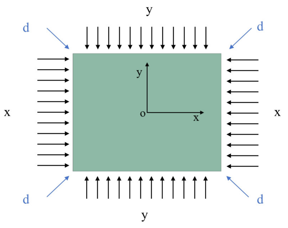
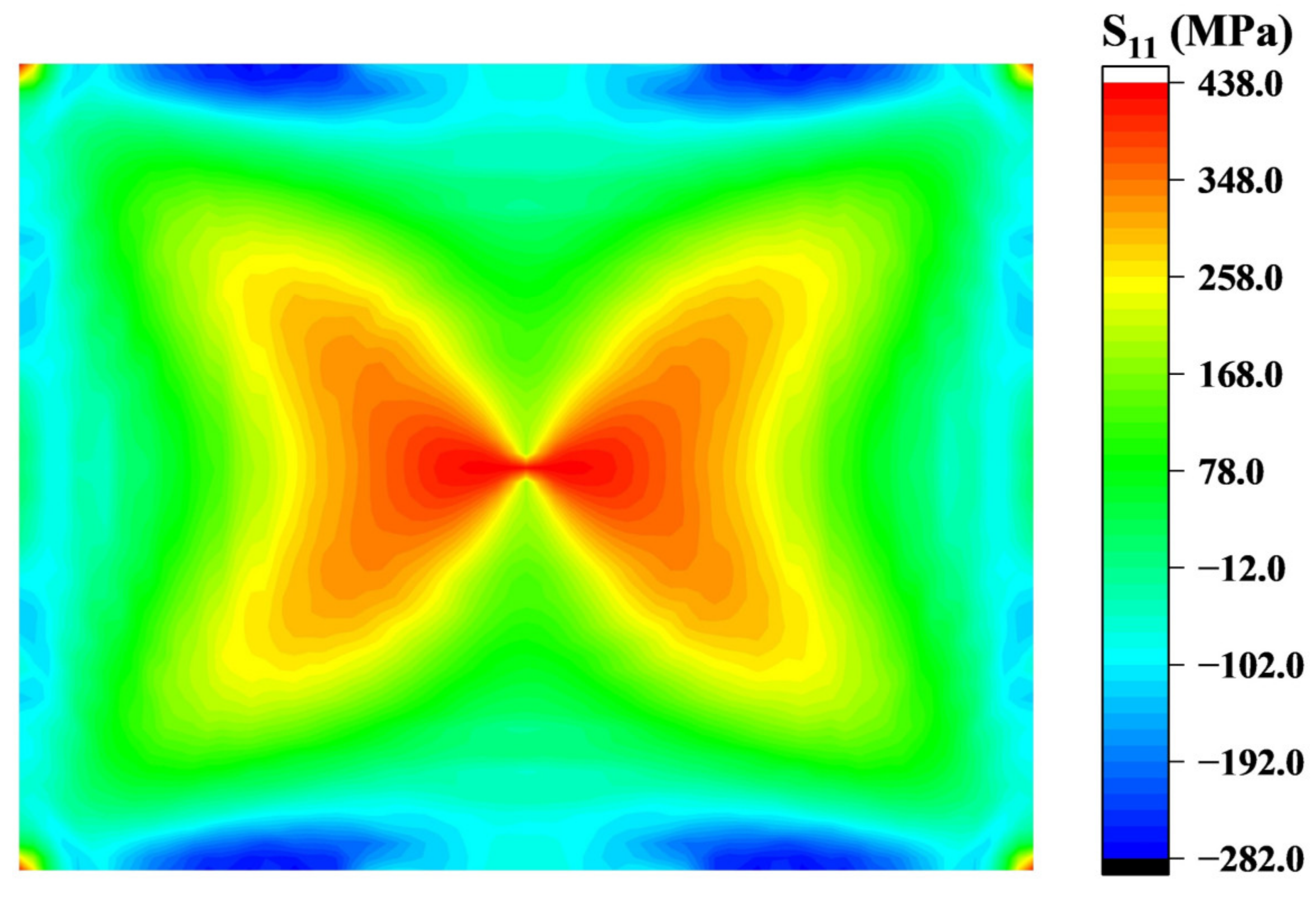
2. Bending Theory
3. Setup of Simulation Parameters
3.1. Elastic Modulus for Polymer Films
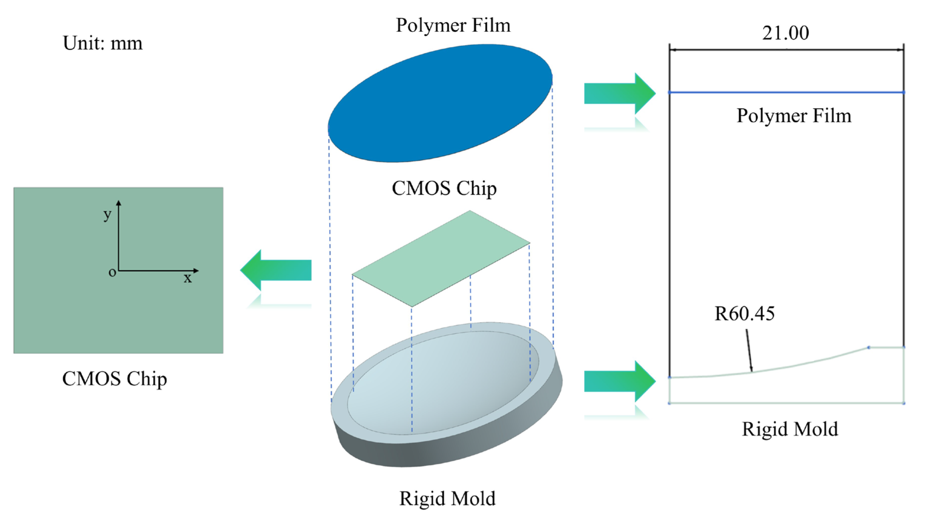
3.2. Parameters of CMOS Chips
3.3. Selection of Mould Materials
4. Process of Bending
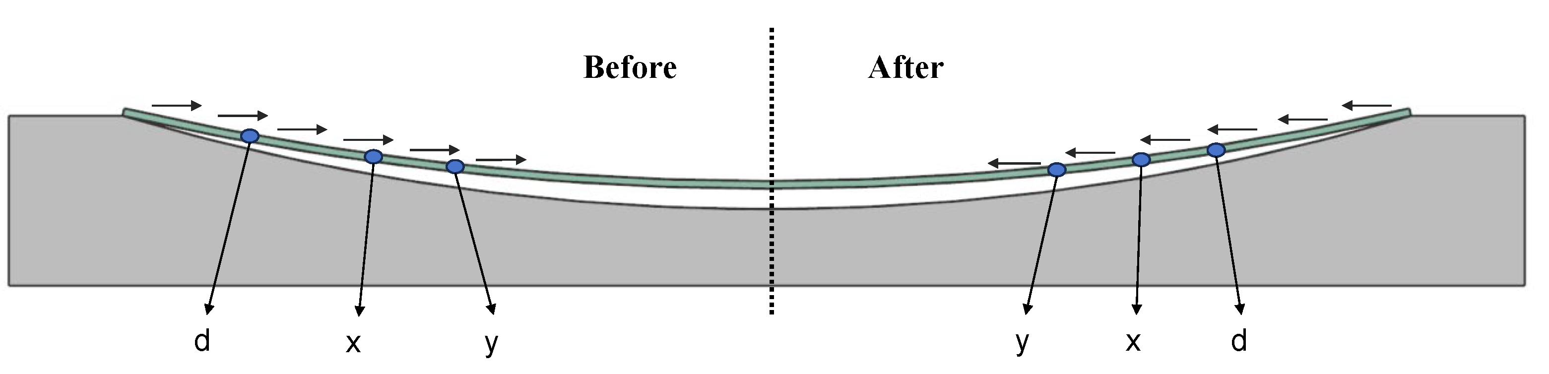
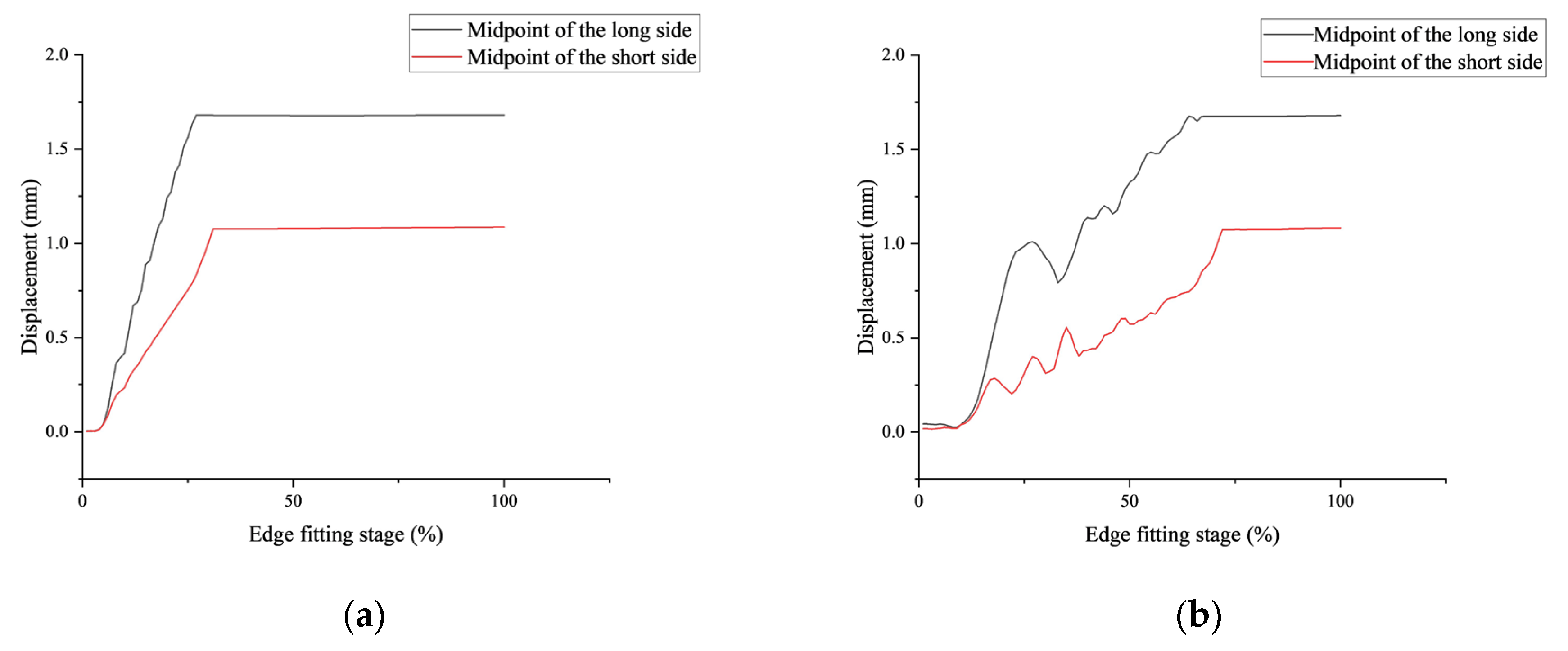
4.1. Edge Fitting Stage
4.1.1. Edge–Middle Contact
4.1.2. Edge Fitting
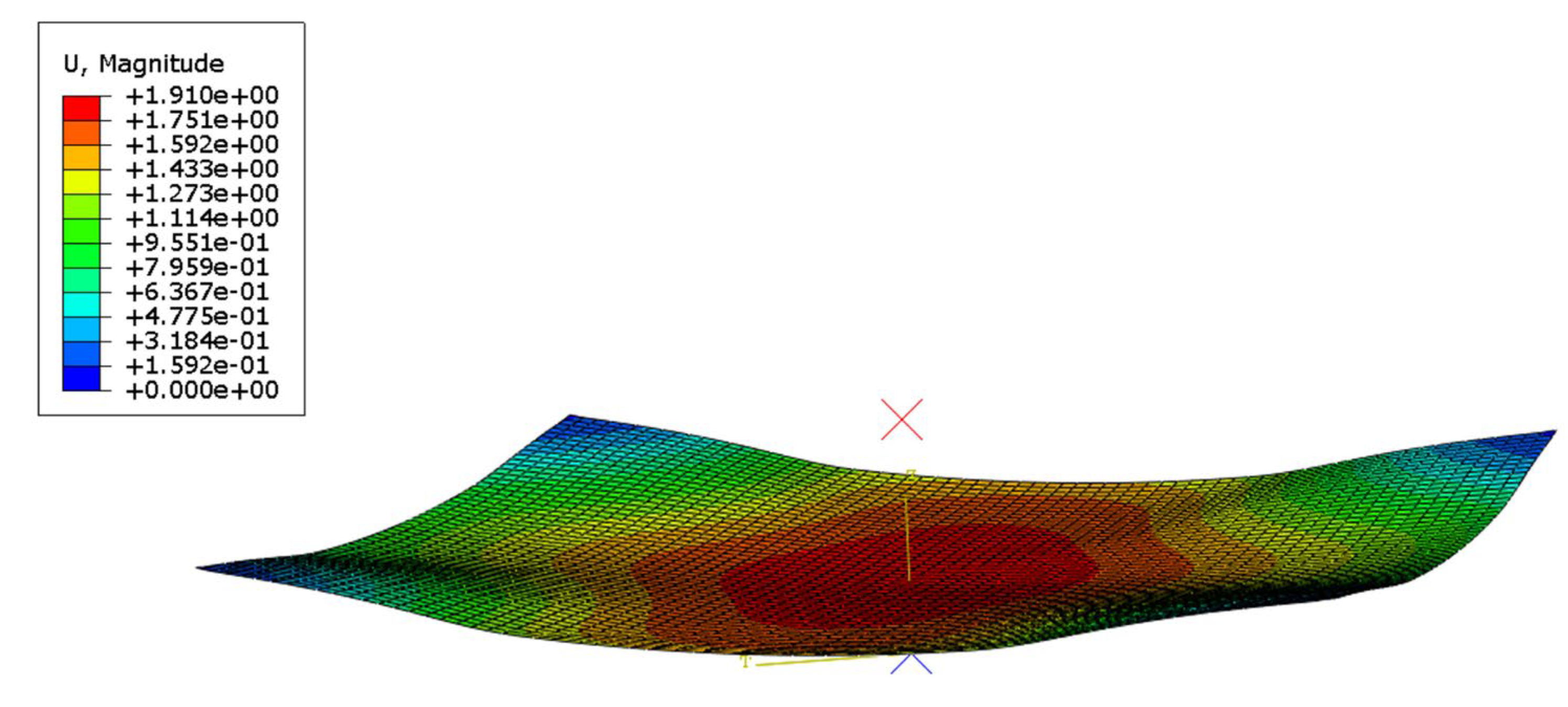
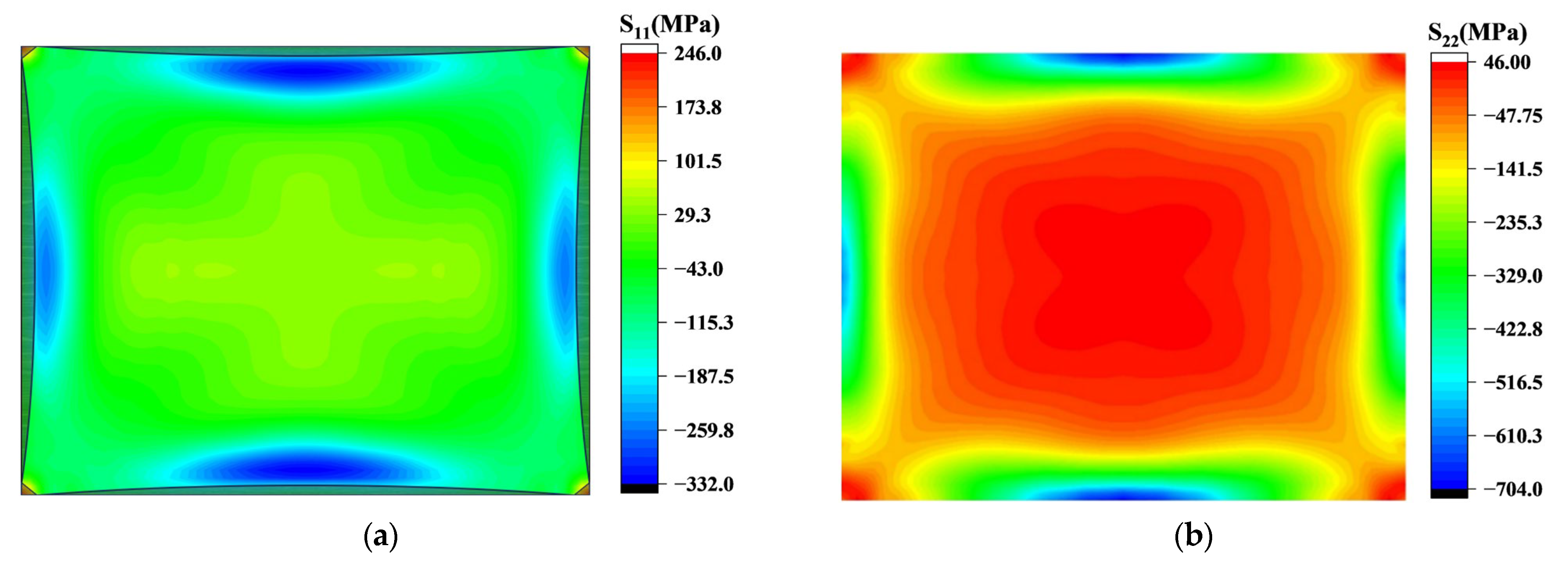
4.2. Molding Stage
5. Summarize the Outlook
Author Contributions
Funding
Institutional Review Board Statement
Informed Consent Statement
Data Availability Statement
Conflicts of Interest
References
- Lee, J.U.; Yu, S.M. Analytic Design Procedure of Three-mirror Telescope Corrected for Spherical Aberration, Coma, Astigmatism, and Petzval Field Curvature. J. Opt. Soc. Korea 2009, 13, 184–192. [Google Scholar] [CrossRef]
- Chung, T.; Lee, Y.; Yang, S.-P.; Kim, K.; Kang, B.-H.; Jeong, K.-H. Mining the Smartness of Insect Ultrastructures for Advanced Imaging and Illumination. Adv. Funct. Mater. 2018, 28, 1705912. [Google Scholar] [CrossRef]
- Wang, Y.; Fu, L.; Chen, P.; Liu, X.; Liu, W.; Lin, L. Design of Schmidt Corrector Plate for Cancelling Aberrations of Spectrometers. Acta Opt. Sin. 2019, 39, 0512006. [Google Scholar] [CrossRef]
- Zhang, X.; Fu, Q. The Technological Investigation on Space Optical Systems Development. Spacecr. Recovery Remote Sens. 2011, 32, 29–35. [Google Scholar]
- Lee, G.J.; Nam, W.I.; Song, Y.M. Robustness of an artificially tailored fisheye imaging system with a curvilinear image surface. Opt. Laser Technol. 2017, 96, 50–57. [Google Scholar] [CrossRef]
- Ko, H.C.; Stoykovich, M.P.; Song, J.; Malyarchuk, V.; Choi, W.M.; Yu, C.-J.; Geddes, J.B., III; Xiao, J.; Wang, S.; Huang, Y.; et al. A hemispherical electronic eye camera based on compressible silicon optoelectronics. Nature 2008, 454, 748–753. [Google Scholar] [CrossRef]
- Liu, H.; Huang, Y.; Jiang, H. Artificial eye for scotopic vision with bioinspired all-optical photosensitivity enhancer. Proc. Natl. Acad. Sci. USA 2016, 113, 3982–3985. [Google Scholar] [CrossRef]
- Gao, W.; Xu, Z.; Han, X.; Pan, C. Recent advances in curved image sensor arrays for bioinspired vision system. Nano Today 2022, 42, 101366. [Google Scholar] [CrossRef]
- Chen, S.; Chen, J.; Zhang, X.; Li, Z.-Y.; Li, J. Kirigami/origami: Unfolding the new regime of advanced 3D microfabrication/nanofabrication with “folding”. Light Sci. Appl. 2020, 9, 75. [Google Scholar] [CrossRef]
- Chen, H.; Zhang, X.-L.; Zhang, Y.-Y.; Wang, D.; Bao, D.-L.; Que, Y.; Xiao, W.; Du, S.; Ouyang, M.; Pantelides, S.T.; et al. Atomically precise, custom-design origami graphene nanostructures. Science 2019, 365, 1036–1040. [Google Scholar] [CrossRef]
- Silva, C.A.; Lv, J.; Yin, L.; Jeerapan, I.; Innocenzi, G.; Soto, F.; Ha, Y.-G.; Wang, J. Liquid Metal Based Island-Bridge Architectures for All Printed Stretchable Electrochemical Devices. Adv. Funct. Mater. 2020, 30, 2002041. [Google Scholar] [CrossRef]
- Fan, D.; Lee, B.; Coburn, C.; Forrest, S.R. From 2D to 3D: Strain- and elongation-free topological transformations of optoelectronic circuits. Proc. Natl. Acad. Sci. USA 2019, 116, 3968–3973. [Google Scholar] [CrossRef] [PubMed]
- Dinyari, R.; Rim, S.-B.; Huang, K.; Catrysse, P.B.; Peumans, P. Curving monolithic silicon for nonplanar focal plane array applications. Appl. Phys. Lett. 2008, 92, 169901. [Google Scholar] [CrossRef]
- Gu, L.; Poddar, S.; Lin, Y.; Long, Z.; Zhang, D.; Zhang, Q.; Shu, L.; Qiu, X.; Kam, M.; Javey, A.; et al. A biomimetic eye with a hemispherical perovskite nanowire array retina. Nature 2020, 581, 278–282. [Google Scholar] [CrossRef]
- Li, S.-X.; Xia, H.; Sun, X.-C.; An, Y.; Zhu, H.; Sun, H.-B. Curved Photodetectors Based on Perovskite Microwire Arrays via In Situ Conformal Nanoimprinting. Adv. Funct. Mater. 2022, 32, 2202277. [Google Scholar] [CrossRef]
- Dumas, D.; Fendler, M.; Baier, N.; Primot, J.; le Coarer, E. Curved focal plane detector array for wide field cameras. Appl. Opt. 2012, 51, 5419–5424. [Google Scholar] [CrossRef] [PubMed]
- Gregory, J.A.; Smith, A.M.; Pearce, E.C.; Lambour, R.L.; Shah, R.Y.; Clark, H.R.; Warner, K.; Osgood, R.M., 3rd; Woods, D.F.; DeCew, A.E.; et al. Development and appHuHucation of spherically curved charge-coupled device imagers. Appl. Opt. 2015, 54, 3072–3082. [Google Scholar] [CrossRef] [PubMed]
- Chambion, B.; Nikitushkina, L.; Gaeremynck, Y.; Jahn, W.; Hugot, E.; Moulin, G.; Getin, S.; Vandeneynde, A.; Henry, D. Tunable Curvature of Large Visible CMOS Image Sensors: Towards New Optical Functions and System Miniaturization. In Proceedings of the 2016 IEEE 66th Electronic Components and Technology Conference (ECTC), Las Vegas, NV, USA, 31 May—3 June 2016; pp. 178–187. [Google Scholar]
- Guenter, B.; Joshi, N.; Stoakley, R.; Keefe, A.; Geary, K.; Freeman, R.; Hundley, J.; Patterson, P.; Hammon, D.; Herrera, G.; et al. Highly curved image sensors: A practical approach for improved optical performance. Opt. Express 2017, 25, 13010–13023. [Google Scholar] [CrossRef]
- Thomsen, E.V.; Reck, K.; Skands, G.; Bertelsen, C.; Hansen, O. Silicon as an anisotropic mechanical material: Deflection of thin crystalline plates. Sens. Actuators A-Phys. 2014, 220, 347–364. [Google Scholar] [CrossRef]
- Hopcroft, M.A.; Nix, W.D.; Kenny, T.W. What is the Young’s Modulus of Silicon? J. Microelectromechanical Syst. 2010, 19, 229–238. [Google Scholar] [CrossRef]
- Cheng, J.; Niu, Y.; Wang, J.; Qu, P.; Wang, K.; Bai, X. Analysis of anisotropic mechanical properties of monocrystalline silicon callow. J. Harbin Inst. Technol. 2019, 51, 16–23. [Google Scholar] [CrossRef]
- Masteghin, M.G.; Tong, V.; Schneider, E.B.; Underwood, C.C.L.; Peach, T.; Murdin, B.N.; Webb, R.P.; Clowes, S.K.; Cox, D.C. Stress-strain engineering of single-crystalline silicon film by ion implantation: Towards direct-gap group-IV semiconductors. Phys. Rev. Mater. 2021, 5, 124603. [Google Scholar] [CrossRef]
- Chen, M.; Pethö, L.; Sologubenko, A.S.; Ma, H.; Michler, J.; Spolenak, R.; Wheeler, J.M. Achieving micron-scale plasticity and theoretical strength in Silicon. Nat. Commun. 2020, 11, 2681. [Google Scholar] [CrossRef] [PubMed]


| E | 10 | 100 | 300 | 500 | 800 | 1200 | 3000 |
| Mises | 1375 | 1375 | 1373 | 1375 | 1377 | 1375 | 1376 |
Disclaimer/Publisher’s Note: The statements, opinions and data contained in all publications are solely those of the individual author(s) and contributor(s) and not of MDPI and/or the editor(s). MDPI and/or the editor(s) disclaim responsibility for any injury to people or property resulting from any ideas, methods, instructions or products referred to in the content. |
© 2024 by the authors. Licensee MDPI, Basel, Switzerland. This article is an open access article distributed under the terms and conditions of the Creative Commons Attribution (CC BY) license (https://creativecommons.org/licenses/by/4.0/).
Share and Cite
Zheng, W.; Li, C.; Hu, J.; Guo, L. Investigation of the Bending Process and Theory in Free-Boundary Pneumatic Film-Forming for Curved Image Sensors. Sensors 2024, 24, 6428. https://doi.org/10.3390/s24196428
Zheng W, Li C, Hu J, Guo L. Investigation of the Bending Process and Theory in Free-Boundary Pneumatic Film-Forming for Curved Image Sensors. Sensors. 2024; 24(19):6428. https://doi.org/10.3390/s24196428
Chicago/Turabian StyleZheng, Weihan, Chunlai Li, Jiangcheng Hu, and Liang Guo. 2024. "Investigation of the Bending Process and Theory in Free-Boundary Pneumatic Film-Forming for Curved Image Sensors" Sensors 24, no. 19: 6428. https://doi.org/10.3390/s24196428