Abstract
This paper presents aspects related to the indirect thermographic measurement of a C2M0280120D transistor in pulse mode. The tested transistor was made on the basis of silicon carbide and is commonly used in many applications. During the research, the pulse frequency was varied from 1 kHz to 800 kHz. The transistor case temperature was measured using a Flir E50 thermographic camera and a Pt1000 sensor. The transistor die temperature was determined based on the voltage drop on the body diode and the known characteristics between the voltage drop on the diode and the temperature of the die. The research was carried out in accordance with the presented measuring standards and maintaining the described conditions. The differences between the transistor case temperature and the transistor die temperature were also determined based on simulation work performed in Solidworks 2020 SP05. For this purpose, a three-dimensional model of the C2M0280120D transistor was created and the materials used in this model were selected; the methodology for selecting the model parameters is discussed. The largest recorded difference between the case temperature and the junction temperature was 27.3 °C. The use of a thermographic camera allows the transistor’s temperature to be determined without the risk of electric shock. As a result, it will be possible to control the C2M0280120D transistor in such a way so as not to damage it and to optimally select its operating point.
1. Introduction
Transistors are among the electronic components from which electronic devices are built [1]. They consist of a die placed on a base plate made of a well-conducting metal, which, in many cases, is copper. The die is encapsulated inside epoxy resin, and connections to die are possible using leads, commonly called “legs”, which are often made of the same material as the base plate. Only one of the leads is directly attached to the base plate. The remaining two leads are placed in the epoxy resin and connected to the die using thin bond wires. The parts of the base plate and leads that are not placed under the epoxy resin layer are covered with a thin layer of tin [2,3]. The dimensions of the base plate, leads, and the epoxy resin layer depend on the type of case used; the most commonly used cases are TO 220 and TO 247. The dimensions of the electronic cases are standardized [4]. In the remainder of this article, the term “transistor” should be understood together with the case in which it is placed.
The most popular materials from which transistor dies are made include silicon (Si), silicon carbide (SiC), and gallium nitride (GaN). Transistors made of these materials differ in their properties [5]. Electronic components made on the basis of silicon reach the limit operating parameters resulting from the theoretical limitations of the material used. For this reason, electronic components based on SiC and GaN materials, called wide band gap (WBG) semiconductors, are becoming more and more popular. They feature better electrical, mechanical, and thermal properties than the electronic components made on the basis of Si. Replacing Si with WBG semiconductors increases the breakdown voltages, operating temperatures, and switching frequency and reduces switching losses [6]. Elements made on the basis of SiC deserve special attention. Compared to Si elements, those made on the basis of SiC have higher breakdown voltage values and higher thermal conductivity [7]. Another feature of this type of semiconductor is low ON-resistance [8].
Metal oxide semiconductor field effect transistors (MOSFETs) made on the basis of SiC are used in the construction of high conversion ratio converters (HCRCs) [9], traction converters [10], wind turbine converters [11], motor drives for electric vehicles [12], and DC–DC step-up converters [13]. The operational reliability of these devices is related to the operational reliability of the SiC MOSFETs placed inside them [14]. Due to the construction of the die area and the width of the gate oxide, they are susceptible to transient-overloading or short-circuit events [15]. Other examples of SiC MOSFET damage are related to long-term exposure to high temperature, which can cause interlayer dielectric erosion, electrode delamination, gate-oxide breakdown [16], and bond-wire lift-off and solder cracks [17,18].
The temperature value of SiC MOSFETs depends, among other things, on their switching frequency [19]. In turn, the switching frequency depends on the operating characteristics of the device in which the transistor is placed and on its energy efficiency [20]. A good example is the converter. In high-power converters, lower switching frequencies are often used to minimize switching losses and increase energy efficiency [21]. In turn, in low-power converters, higher switching frequencies are usually used, which may lead to smaller converter sizes and better regulation [22]. The higher the switching frequency is, the shorter is the switching time of SiC-based MOSFETs. During switching, rapid changes in voltage and current occur, which leads to power losses and heat generation. Therefore, the switching frequency has a direct impact on heat generation in the transistor [23].
The switching frequency of a SiC MOSFET affects the temperature of its die. In turn, the operation of the die at excessively high temperature may damage the transistor. For this reason, it is necessary to monitor the die temperature of the transistor, Tj. In the literature, is possible to find three groups of methods that make this possible: electrical, contact, and non-contact methods [24].
Electrical methods use a selected parameter whose value depends on Tj. This parameter is called the temperature-sensitive parameter (TSP) [25]. An example of a TSP that is used to determine the die temperature of a transistor is the drop voltage across the body diode. Knowing the relationship between TSP and Tj, it is possible to determine the Tj value based on the measured TSP value. The relationship between TSP and Tj is individual for each transistor. Additionally, its determination requires removing the transistor from the device in which it was installed and placing it in the measurement system. For this reason, this method is not suitable for real-time monitoring of Tj values [26].
Contact methods involve applying a temperature sensor to the transistor package (also called a ‘case’ in the literature) or directly to the die transistor. There is thermal resistance of an unknown value between the temperature sensor case and the transistor case (or die). Additionally, touching the transistor (or die) case with the temperature sensor causes a local disturbance of the temperature distribution. Part of the transistor case is made of metal; therefore, incorrect application of the temperature sensor (especially when placed in a metal case) may cause electric shock [27].
Non-contact methods are based on the absorption of infrared radiation emitted from the surface of the transistor case (indirect non-contact method) or through the transistor die (direct non-contact method). One of these methods is infrared thermography, which is considered safe, as it poses no risk of electric shock (e.g., as a result of touching a metal temperature sensor based on a plate or a radiator to which a transistor is attached). The direct method requires opening the transistor case. It is difficult to close the opened case. For this reason, it is not suitable for real-time application. The use of the indirect non-contact method consists of two steps: measuring the temperature of the transistor case (Tc) and determining the difference between Tc and Tj. Tc can be measured using a pyrometer and a thermographic camera. The use of a thermographic camera makes it possible to determine the temperature distribution on the surface of the transistor case. The differences between Tc and Tj can be determined using the finite element method. Knowing the value of the thermographic measurement of the temperature of the transistor case and the relationship between Tc and Tj, it is possible to determine the value of Tj in real time [28,29].
After analyzing the available sources, no studies were found on the indirect thermographic temperature measurement of a SiC MOSFET, the temperature of which increases due to the increase in the switching frequency. For this reason, it was decided to undertake research that would result in the development of a method enabling the indirect thermographic measurement of the SiC MOSFET die temperature and monitoring that temperature at variable switching frequencies.
2. Tested Transistor, Methodology, and Measurement System
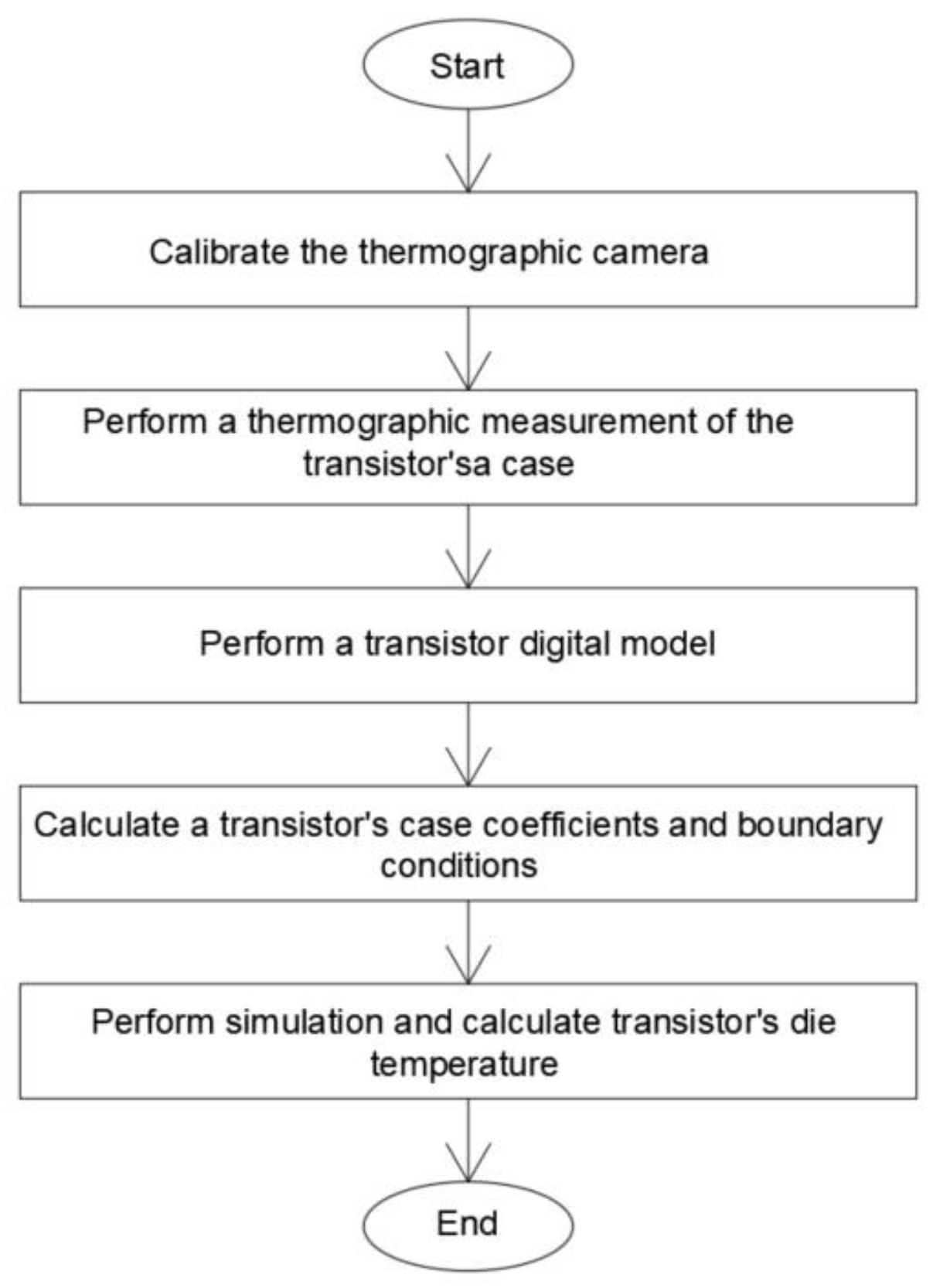
The indirect thermographic measurement of the transistor temperature die consists of two parts. The first part consists of performing a thermographic measurement of the transistor case temperature, Tc. The second part consists of determining the transistor die value Tj using simulation work. The method of performing a thermographic measurement of Tc is described in Section 2.1. The value of TPt1000, which is used to verify the Tc value, is also determined and described in Section 2.1. The method used to determine the Tj value based on simulation work is described in Section 2.2. The method for determining the Tjd value, which is used to verify the Tj value (determined based on simulation work), is also described in Section 2.2. The algorithm for the procedure is presented in Figure 1.
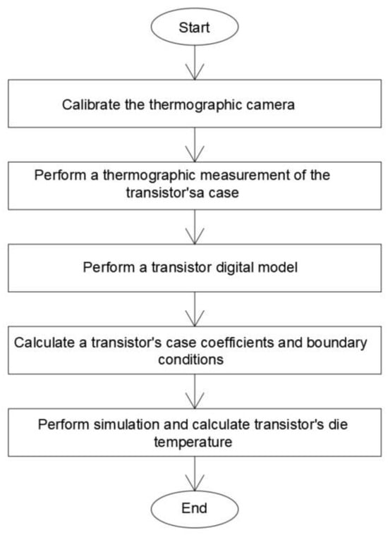
Figure 1.
Algorithm for performing indirect thermographic temperature measurements of a transistor.
2.1. Tested Transistor and Measurement System
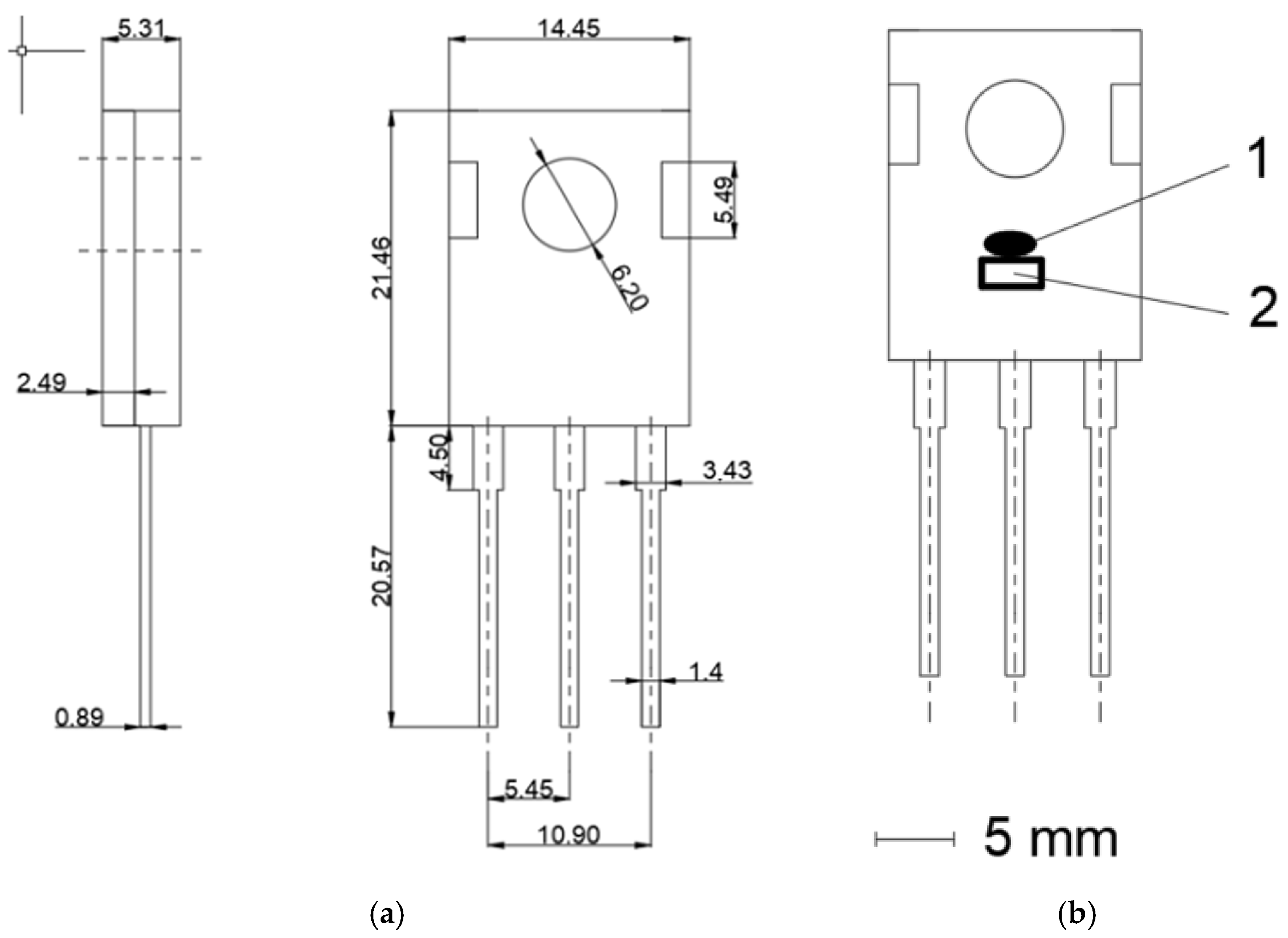
The model C2M0280120D (Cree Inc., Durham, NC, USA) transistor was selected for testing. This transistor is described by the following parameters: VDSmax = 1200 V (for VGS = 0 V, ID = 100 µA), VGSmax = −10/+25 V, ID = 10 A (for VGS = 20 V, Tc = 25 °C), ID = 6 A (for VGS = 20 V, Tc = 100 °C), and IDpulse = 20A. The external dimensions of the transistor and schematics are shown in Figure 2. Three randomly selected C2M0280120D transistors from the same series were selected to carry out the work.
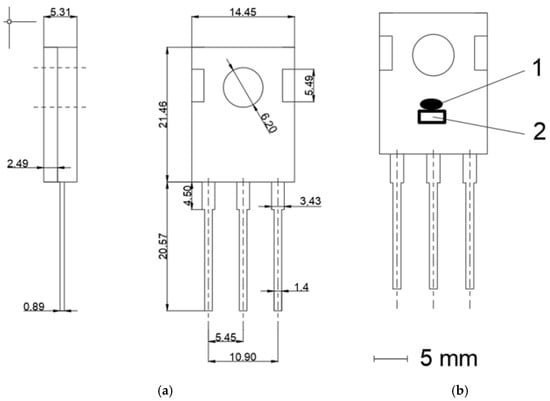
Figure 2.
(a) External dimensions of transistor model C2M0280120D in a TO 247 case. (b) Schematic of C2M0280120D in a TO 247 case. A marker was painted on the case using Velvet Coating 811-21 paint (1) and a Pt1000 sensor was glued onto the case (2).
Pt1000 sensors in an SMD 6203 case (Reichelt electronics GmbH & Co. KG, Sande, Germany) were glued to the case of each transistor [30]. For this purpose, WLK 5 glue with a known thermal conductivity value of k = 0.836 W/mK (Fischer Elektronik GmbH & Co. KG, Lüdenscheid, Germany) was used [31]. Additionally, next to the Pt1000 sensor, a measurement marker was painted on the transistor case. Velvet Coating 811-21 (Nextel, Hamburg, Germany) paint was used for this purpose with a known emissivity coefficient value ε ranging from 0.970 to 0.975 for temperatures within the range from –36 °C to 82 °C. The uncertainty with which the emissivity coefficient value was determined was 0.004 [32].
The transistor prepared in this way was placed in a station where the measuring device was a Flir E50 Thermographic Camera (Flir, Wilsonville, OR, USA) [33]. The selected Flir E50 thermographic camera was equipped with a matrix from an uncooled IR detector (7.5–13 µm) with a resolution of 240 × 180 pixels and an instantaneous field of view (IFOV) value of 1.82 mrad. The noise equivalent differential temperature (NEDT) value of this camera was 50 mK. An additional Close-up 2× lens (T197214, Flir, Wilsonville, OR, USA) was attached to the camera lens [34]. As a consequence, it was possible to obtain an IFOV value of 67 µm for the above-mentioned detector array (240 × 180 pixels) (thermographic camera with the additional lens). Before starting the work, the correctness of the indications of the camera used was verified using the IRS Calilux thermographic camera calibration standard (AT—Automation Technology GmbH, Bad Oldesloe, Germany) [35].
The thermographic camera prepared in this way was placed together with the tested C2M0280120D transistor in a chamber made of plexiglass. The external dimensions of the chamber were 45 cm × 35 cm × 35 cm. The internal dimensions of the chamber were 40 cm × 30 cm × 30 cm. The difference resulted from two reasons: the thickness of the plexiglass used (3 mm) and the thickness of the material (black foam made of polyurethane) lining the internal walls of the chamber. The foam used is characterized by porous structure, and every single pore of the foam resembles the black body cavity model. As a consequence, the material used was characterized by having a high emissivity factor ε = 0.95 [36].
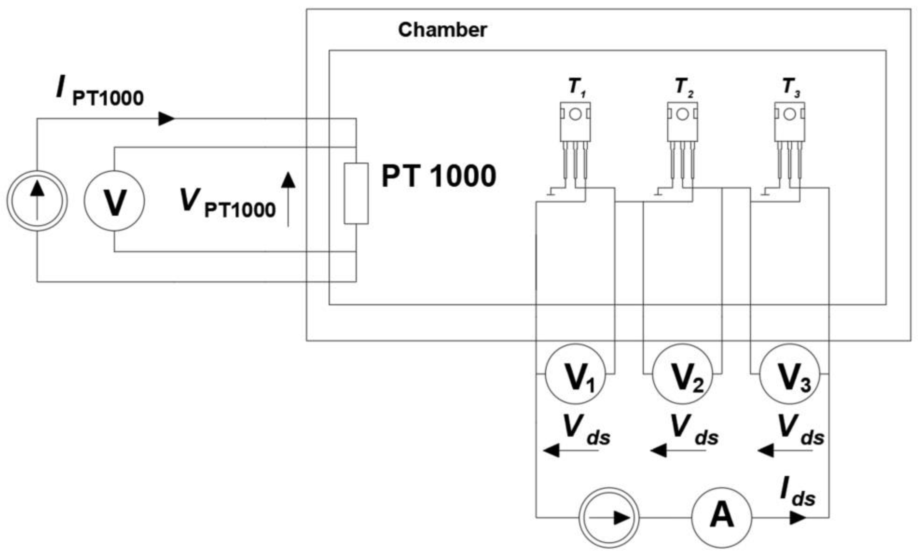
The distance d between the tested transistor and the additional lens was adjusted using a stepper motor. In turn, the stepper motor was controlled using a Siemens S7-1200 PLC controller (Siemens AG, Munich, Germany) [37]. A block diagram of the constructed stand is shown in Figure 3.
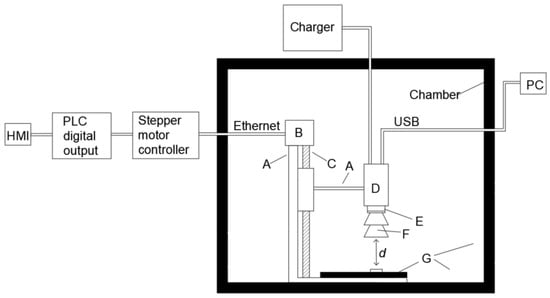
Figure 3.
Thermographic camera and observed transistor placed in the prepared chamber. A—stand, B—stepper motor, C—screw, D—thermographic camera, E—thermographic camera lens, F—additional thermographic camera lens, G—polyurethane foam, d—distance between the tested transistor and the additional lens.
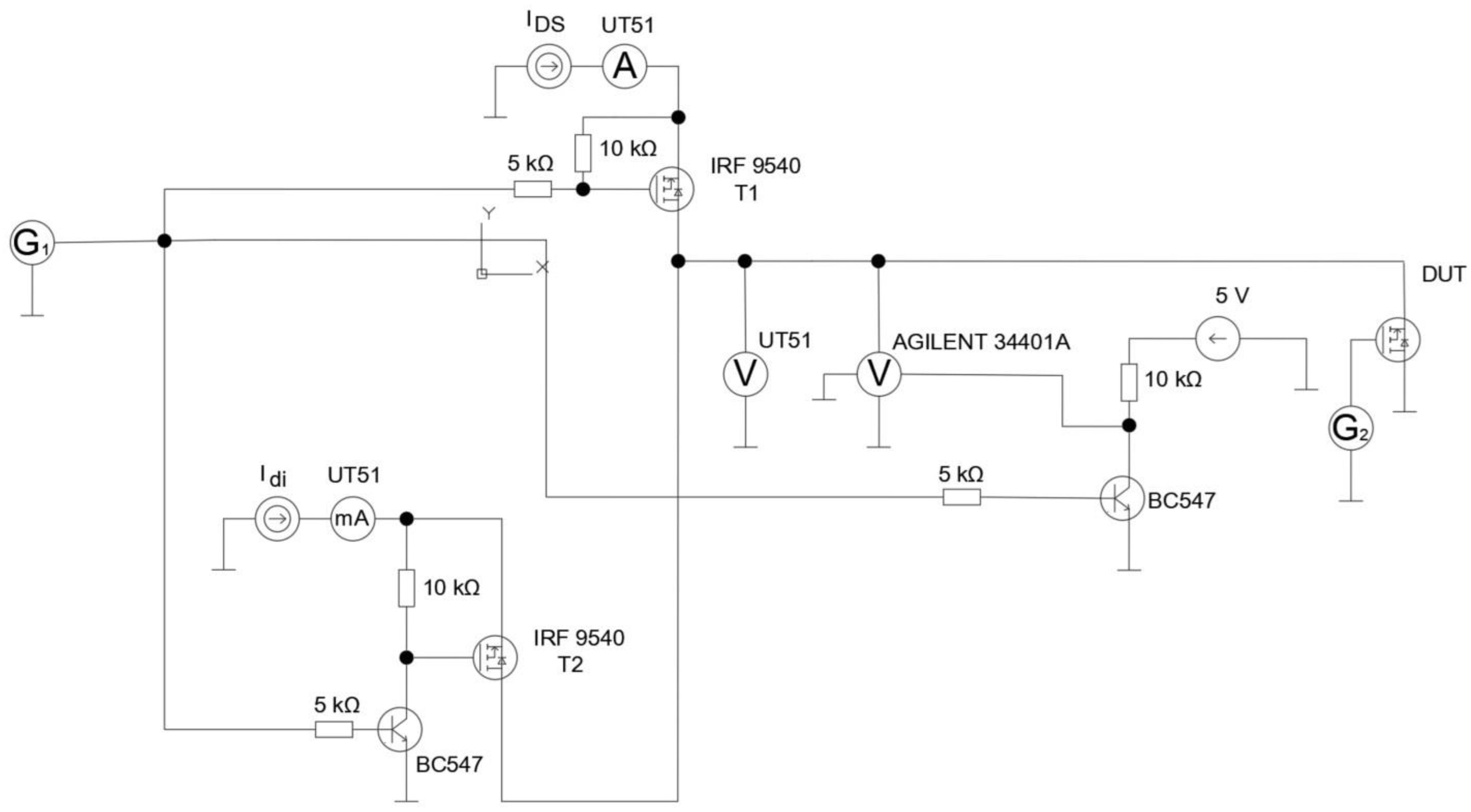
The observed transistor was connected to a circuit that allowed its switching frequency to be changed. The circuit diagram is shown in Figure 4. In this circuit, the transistor T1 was turned on by the generator G1 for 20 s. As a result, the load current IDS flowed through the tested transistor. During this time, the voltage drop between the drain and the source VDS was measured using an Agilent 34401A voltmeter. In the next step, the same generator G1 turned on transistor T2, allowing the flow of the measuring current Idi for 200 ms. This operation allowed estimating the die temperature based on the automatic measurement of the drop voltage Vfd on the diode and the known characteristic between the drop voltage value and the die temperature. During the entire testing process, the tested transistor (DUT) was pulse-controlled using the G2 generator with a PWM waveform with a duty cycle of 50% and a frequency in the range from 1 kHz to 50 kHz.
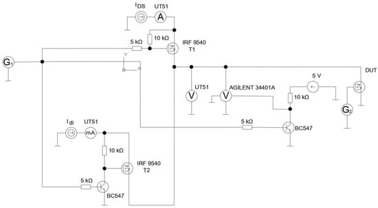
Figure 4.
Diagram of the circuit enabling the evaluation of the influence of the switching frequency changes of the transistor on the temperature of its die. DUT—device under test, i.e., the tested transistor.
The case of the tested transistor, in which the switching frequency was changed, was observed using a thermographic camera. During the tests, first, for a given value of the current IDS flowing through the die and a given switching frequency fT, the temperature of the case (Tc) was measured using a thermographic camera. We then waited until its value increased and stabilized at a specified level. When it was found that the Tc value had stabilized, its thermographic measurement was performed. At the same time, Tc was measured using a Pt1000 sensor, which was glued to the case near the thermographic measurement point (Figure 2). After the measurement was performed, the switching frequency fT of the transistor was changed for the same ID current value. The fT setting was changed for selected values, ranging from 1 kHz to 800 kHz.
2.2. Finite Element Analysis and Measurement of Die Temperature
The relationship between Tc and Tj was determined using finite element analysis (FEA), which is a numerical method used to solve problems in engineering and mathematical physics [38]. The software applied in the work performed was Solidworks 2020 SP05 (Dassault Systèmes, Vélizy-Villacoublay, France), which uses FEA, and the simulation was completed with the use of this software.
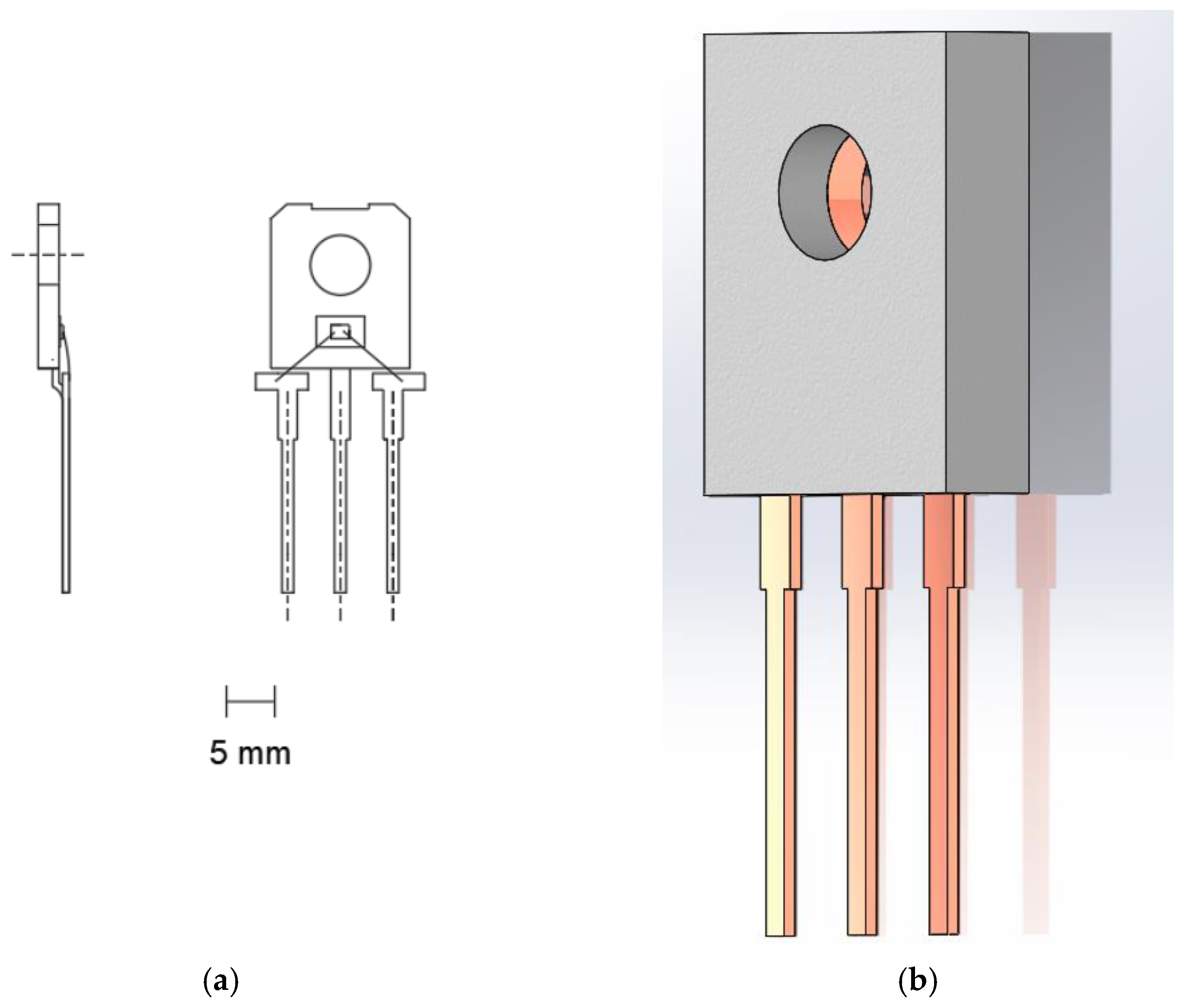
The simulation could be carried out after the transistor model had been constructed. Making the model required knowledge of its structure and internal dimensions. In order to determine these, the case of the tested transistor was opened and its interior was measured. For this purpose, a microscope equipped with a Cam 3.3 MP camera (Motic, Xiamen, China) was used. The microscope with the camera was calibrated using a special calibration glass. Based on the measurements taken, a three-dimensional model of the tested transistor was created. The model was created in Solidworks 2020 SP05 software. The created model and internal dimensions of the tested transistor C2M0280120D are shown in Figure 5.
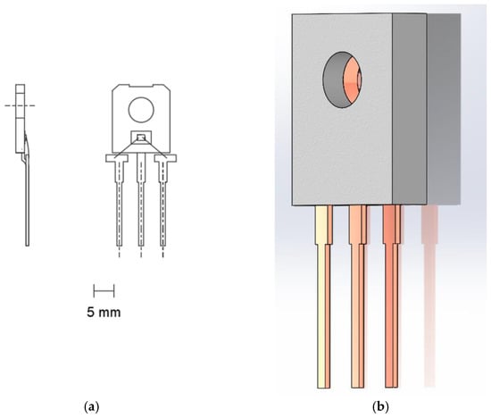
Figure 5.
(a) Internal dimensions (see Figure 2 for details) and (b) three-dimensional model of the C2M0280120D transistor.
After creating the model, all of its elements were assigned the material from which it was made, along with the thermal conductivity values k. Next, the simulation was started in the Solidworks 2020 SP05 environment. In the initial stage, we checked whether the temperature distribution (measured at the surface) changes after removing individual parts of the model (e.g., leads). The temperature distribution was also checked, depending on the given mesh size. After simplifying the model and selecting the mesh size, it was possible to determine the Tj value based on the simulation work.
The die temperature (Tj) of the tested transistors obtained as a result of simulation work was verified for the same conditions using the electrical method. In order to perform a reliable temperature measurement of the die using the electrical method, it was necessary to select the appropriate temperature-sensitive parameter (TSP). The voltage drop Vfd across the body diode was chosen as the TSP. In order to use the TSP to determine the Tj value, the relationship Tj = f(Vfd) had to be determined. For this reason, a measuring system was designed, the main element of which was a climatic chamber. The chamber used allowed for changing the temperature Ta inside it. The Ta value was changed in the range from 20 °C to 180 °C. Additionally, a Pt1000 sensor was placed inside the chamber, which was used to measure the temperature there. The sensor was connected in a four-wire circuit for measuring resistance using the technical method. A current of 100 µA flowed through the sensor.
In order to determine the relationship Tj = f(Vfd), three tested transistors were placed inside the described chamber. They were connected in such a way that the current Idi (Idi = 100 mA) forcing the voltage drop Vfd on the body diode flowed through all diodes of the tested transistors (the body diodes of the three transistors were connected in series). The measurement setup is shown in Figure 6. The Vfd values of all tested transistors were measured using an Agilent 34401A multimeter (Agilent, Santa Clara, CA, USA) [39]. The measurement was performed for a given temperature Ta at the moment when the Vfd voltage value stabilized. The constant values of the Vfd voltage in time indicated that the temperature Ta set in the chamber was equal to the die temperature Tj of the transistors located in this chamber. In turn, the voltage drop VPt1000 on the Pt1000 sensor was measured using a UT51 multimeter (UNI-T, Dongguan City, China) [40].

Figure 6.
Measurement system enabling determination of the relationship Tj = f(Vfd).
2.3. Power Dissipated in Die and Ambient Conditions
The correct simulation work using Solidworks 2020 SP05 requires determining the power P that has been released in the die and defining the boundary condition. The power released in the die can be determined using Equation (1):
where: P—power (in W) dissipated in the die, VDS—drop voltage (in V) between drain and source, IDS—current (in A) flowing between drain and source.
The VDS and IDS values were measured with measurement errors, which can be determined using the UT51 multimeter documentation (UNI-T, Dongguan City, China). Therefore, the p value will also be within the range defined by the measurement error limit ∆P, which can be determined from Equation (2):
where: ∆VDS—limiting error of the VDS value (in V), ∆IDS—limiting error of the IDS value (in A). The ∆IDS and ∆VDS values can be determined using the formulas in the UT51 user manual [40].
The increase in die temperature is related to the distribution of effective power, PRMS, in the die. For this reason, the Equation (3) should be used:
where: t0—beginning of the period, Tk—duration of the period.
The PRMS value is also within the range that is determined by the limiting error ∆PRMS. The limits of the range determined by ∆PRMS can be determined using Equation (2).
The temperature gradient in the radiative heat flux path between the transistor’s die and the transistor’s case can be determined using Equation (4):
where: J—radiative heat flux (W∙m−2), —Nabla operator.
Equation (4) can be written as Equation (5):
where: x—distance between the points where the temperature values of the die and diode case were measured (m), J—radiative heat flux (W∙m−2).
In order to solve Equation (5), we need to separate the differentials that are on the right-hand side of the equation. Consequently, it is possible to integrate the equation on both sides. The constant of integration can be found using Equation (6):
where: xk—end point of the analyzed heat flow path (m), T1—temperature at the starting point of the analyzed heat flow path (K), T2—temperature at the end point of the analyzed heat flow path (K).
Consequently, it is possible to determine Equation (7):
where: Pc—total power (in W) applied to the wall, S—area (m2) of the wall penetrated by J (W∙m−2).
Determining the correct temperature distribution in the transistor’s case (using Solidworks 2020 SP05 Software) requires determining the radiation coefficient hr. The hr coefficient defines the amount of thermal energy transferred to the environment by radiation per unit time, per unit area, and per unit temperature difference between the body radiating energy and the environment. The value of hr can be determined using Equation (8):
where: σ—Stefan–Boltzmann constant equal to 5.67 × 10⁻⁸ (W∙m−2∙K−4), TS—surface temperature (K), Ta—air temperature (K).
It is also necessary to determine the value of the convection coefficient hcf, which defines the amount of thermal energy transferred to the environment by convection per unit time, per unit area, and per unit temperature difference between the body emitting the energy and the environment. To determine the hcf value for a flat surface, Equation (9) can be used:
where: hcf—convection coefficient of flat surfaces, Nu—Nusselt number (-), L—characteristic length in meters (for a vertical wall, this value represents height).
The Nusselt number can be determined using Equation (10).
where: Gr—Grashof number (-), Pr—Prandtl number (-), a and b—dimensionless coefficients. The values of coefficients a and b are provided in Table 1.

Table 1.
Values of coefficients a and b in Equation (10). lam—value for laminar flow, turb—value for turbulent flow.
The Grashof number can be obtained from Equation (11):
where: g—gravitational acceleration (9.8 m∙s−2), α—coefficient of expansion (0.0034 K−1), —air density (1.21 kg∙m−3) at 273.15 K, η—dynamic air viscosity (1.75 × 10⁻⁵ kg∙m−1∙s−1) at 273.15 K.
Prandtl’s number is determined from Equation (12):
where: Pr—Prandtl’s number, c—specific heat of air (1005 J·kg−1·K−1) at 293.15 K.
When the value of the average linear velocity of the fluid flow is greater than 0 m/s, the Reynolds number must also be taken into account, which can be obtained using Equation (13):
where: V—average linear velocity of the fluid flow (m/s).
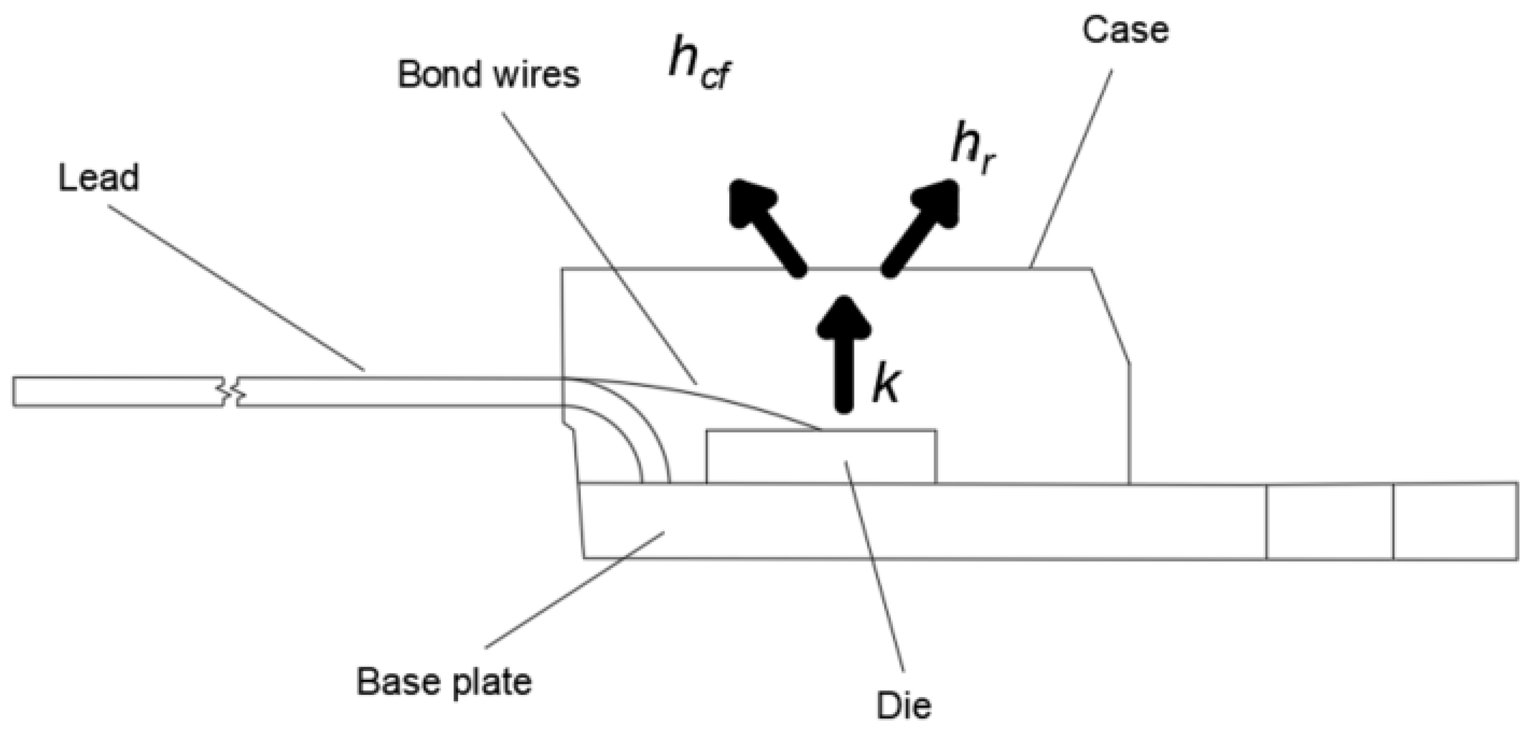
In order to enable a better understanding of the boundary condition, the analyzed heat flow path and its emission by the observed surface (by convection hcf and radiation hr) are shown in Figure 7.
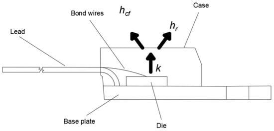
Figure 7.
Analyzed heat flow path and its emission from the observed surface (by convection hcf and radiation hr). Thermal conductivity is designated as k.
2.4. Uncertainties
The method by which the uncertainty of the thermographic temperature measurement Tc can be determined is described in the document Evaluation of the Uncertainty of Measurement in calibration (EA-4/02 M: 2022) [41]. This is a method for determining the uncertainty of type B. In order to use this method, all input quantities Xi that affect the result of the Tc measurement and the range of their variability must be determined. This can be done based on experience and the literature. In this work, the thermographic camera processing equation from publication [42] was used (Equation (14)):
where: Tcam—temperature indicated by the thermographic camera without taking into account the influence of other factors, —Stefan-Boltzmann constant equal to 5.67 × 10⁻⁸ (W∙m−2∙K−4), τa—atmosphere transmittance coefficient, τ1—transmittance of the thermographic camera lens, Ta—air temperature, —reflected temperature, Tl—thermographic camera lens temperature.
The next step is to determine the sensitivity coefficient cs for all input quantities from Equation (14). This is a derivative described in Equation (15):
where: fi—all input quantities from Equation (14).
In order to determine the uncertainty of the Tc value, estimates of xi of the input quantities Xi (for all above input quantities) must be determined. This is possible using Equation (16) (rectangular probability distribution):
where: —upper limit of the input quantity range, —lower limit of the input quantity range.
Then, for each Xi, the uncertainty standard u(xi) should be determined as per Equation (17):
By multiplying the values of u(xi) and cs, we can obtain the uncertainty contribution u(y). The standard uncertainty u(Tc) of the Tc value can be obtained as the square root of the sum of squares of the values of u(y) as per Equation (18):
In order to determine the expanded uncertainty U(Tc), the value of u(Tc) should be multiplied by the coverage factor k.
To determine ∆TPt1000, Equations (19)–(23) can be used:
where: —limit error of VPt1000, —relative error of VPt1000, —limit error of IPt1000, —relative error of IPt1000, —relative error of RPt1000, —limit error of RPt1000, RPt1000—resistance of Pt1000 [42].
Then, by inserting the upper and lower range of ΔRPt1000 into Equation (23), it is possible to obtain the upper and lower range of ΔTPt1000 values:
To determine the ΔVPt1000 and ΔIPt1000 values, the documentation of the multimeter describe in reference [40] can be used.
3. Results
Using the measurement system shown in Figure 6, the relationship Tjd = f(Vfd) was determined. This relationship was approximated by the linear equation y = e∙x + f. As a result, the individual equations Tjd = TC + e∙Vfd + f were obtained for each transistor. The values of the coefficients for each transistor are given in Table 2.
Table 2.
Values of the coefficients e and f of the curves Tjd = TC + e∙Vfd + f of the tested transistors.
Then, each of the tested transistors was connected according to the diagram shown in Figure 4. The black part of the transistor case was observed with a thermographic camera. In order to minimize the factors disturbing the thermographic measurements, the observed transistors and the thermographic camera were placed in a chamber whose connection layout is shown in Figure 3. Additionally, Vfd values were measured using a voltmeter. Using these values, the junction temperature Tjd values were determined based on the previously determined relationship Tjd = f(Vfd) (Table 2). The Tjd values determined in this way are given in Table 2, and sample recorded thermograms are shown in Figure 8.

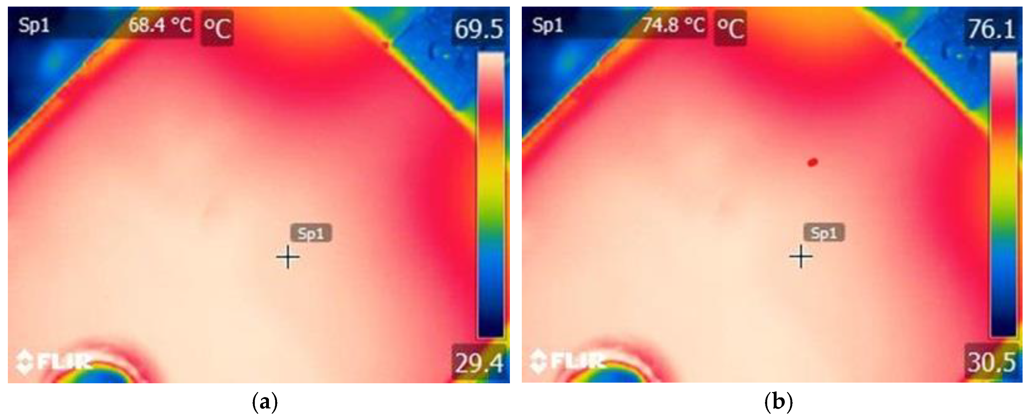
Figure 8.
Examples of recorded thermograms: (a) IDS = 1 A; fT = 1 kHz, (b) IDS = 1 A; fT = 10 kHz. The thermograms were taken before gluing the Pt1000.
In the next stage of the research, simulations were carried out using the FEM method. In the first step, a model of the tested transistor was designed. Materials and thermal conductivity values k are given in Table 3.
Table 3.
Materials specified in the 3D model and their thermal conductivity values k.
The selected values of the convection coefficients hcf of the observed surface (black part of the case) were in the range of 15.3 W/m2 K to 24.8 W/m2 K for the tested temperature ranges.
Additionally, the relationship between the mesh size l specified in the simulation parameters, the duration of a single simulation ts, and the accuracy of the determined temperature values DTS was checked. The obtained results are presented in Table 4.
Table 4.
Mesh size l, simulation duration ts, and temperature values TS obtained during FEM simulation defined in the simulation parameters.
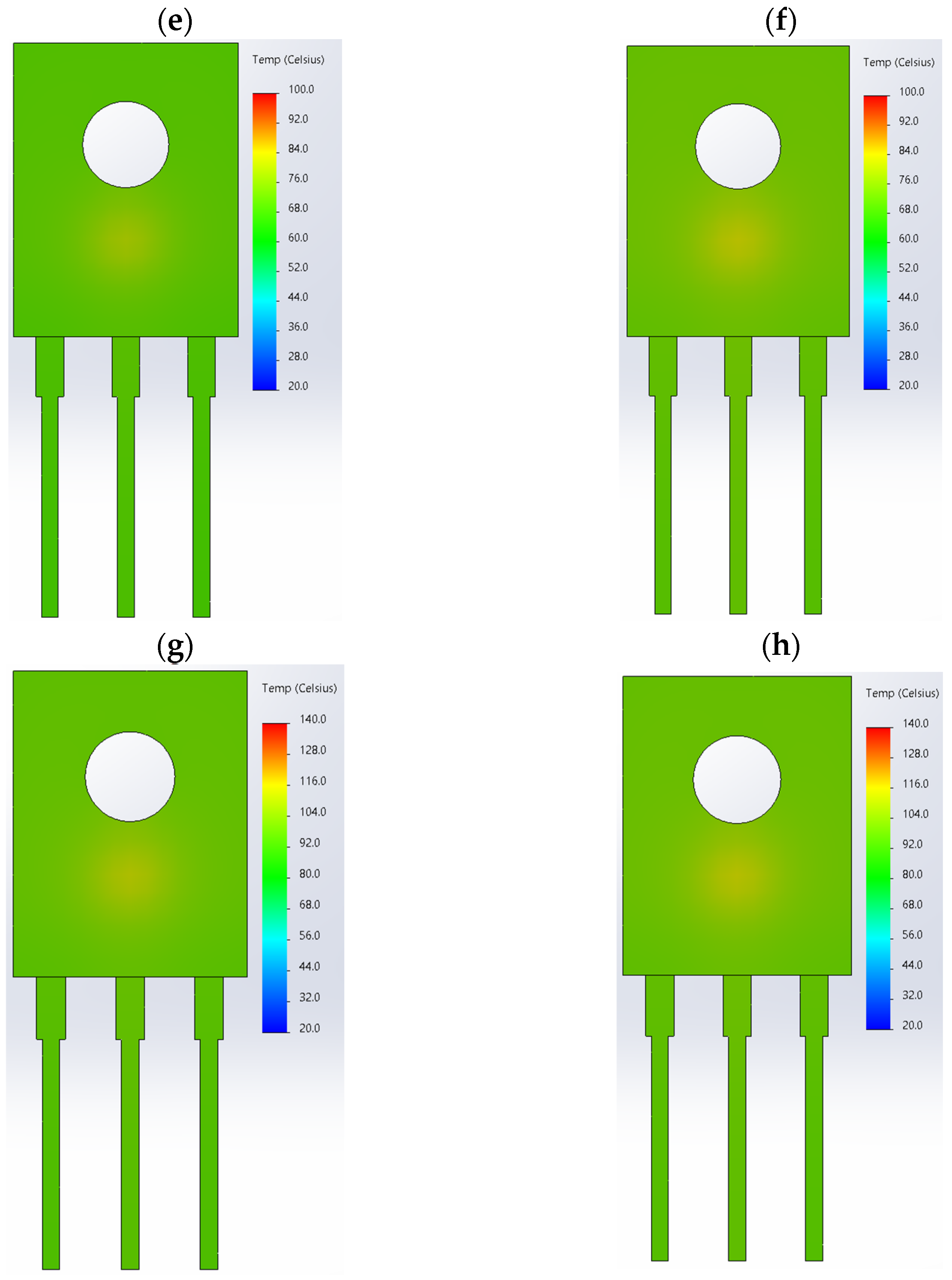
Based on the data presented in Table 4, a mesh size was selected at which the simulation duration was sufficiently short and the accuracy of the ΔTS temperature value obtained as a result of the simulation work was 0.1 °C (Table 4, No. 5). As a result, the TS temperature values obtained from the simulation work were close to the temperature Tc recorded in the thermographic measurement for a given value of the power dissipated in the PRMS transistor. The selected mesh size was l = 1.0 mm. The example temperature distributions obtained from the simulation are shown in Figure 9.
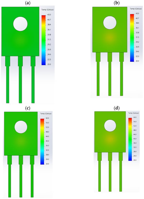
Figure 9.
Examples of temperature distributions obtained from FEM simulations. (a) IDS = 0.25 A, fT = 1 kHz, (b) IDS = 0.25 A, fT = 500 kHz, (c) IDS = 0.5 A, fT = 1 kHz, (d) IDS = 0.5 A, fT = 500 kHz, (e) IDS = 1 A, fT = 1 kHz, (f) IDS = 1 A, fT = 500 kHz, (g) IDS = 1.5A, fT = 1 kHz, (h) IDS = 1.5A, fT = 500 kHz.
Table 5, Table 6, Table 7 and Table 8 present the values of Tc and Tj recorded during measurements and the values of TS (transistor case) obtained as a result of simulation work, depending on the set value of the switching frequency fT of the transistor. The measurements were carried out for four current values.
Table 5.
Transistor case temperature Tc determined from thermographic measurements, junction temperature Tjd determined from the relationship Tjd = f(Vfd), and transistor case temperature TS and junction temperature Tj determined from simulations, depending on the set switching frequency fT. The results were obtained for the current IDSmax = 0.25 A. Tc1 is the Tc value measured for the first transistor, Tc2 is the Tc value measured for the second transistor, and Tc3 is the Tc value measured for the third transistor.
Table 6.
Transistor case temperature Tc determined from the thermographic measurements, junction temperature Tjd determined from the relationship Tjd = f(Vfd), and the transistor case temperature TS and junction temperature Tj determined from simulations, depending on the set switching frequency fT. The results were obtained for the current IDSmax = 0.5 A. Tc1 is the Tc value measured for the first transistor, Tc2 is the Tc value measured for the second transistor, Tc3 is the Tc value measured for the third transistor.
Table 7.
Transistor case temperature Tc determined from thermographic measurements, junction temperature Tjd determined from the relationship Tjd = f(Vfd), and transistor case temperature TS and junction temperature Tj determined from simulations, depending on the set switching frequency fT. The results were obtained for the current IDSmax = 1 A. Tc1 is the Tc value measured for the first transistor, Tc2 is the Tc value measured for the second transistor, Tc3 is the Tc value measured for the third transistor.
Table 8.
Transistor case temperature Tc determined from thermographic measurements, junction temperature Tjd determined from the relationship Tjd = f(Vfd), and transistor case temperature TS and junction temperature Tj determined from simulations, depending on the set switching frequency fT. The results were obtained for the current IDSmax = 1.5 A. Tc1 is the Tc value measured for the first transistor, Tc2 is the Tc value measured for the second transistor, Tc3 is the Tc value measured for the third transistor.
In order to determine the uncertainty of the Tc value, the range of all variables was determined from Equation (14). The adopted ranges of values and the determined xi are given in Table 9.
Table 9.
Values of the variables from Equation (14) and the determined xi.
The Tcam value was also taken into account. The Tcam value limits were selected individually for each case (Tcam ± 2 °C).
Then, using equations from Section 2.4, the standard uncertainty u(xi) and sensitivity coefficient cs (for all input quantities from Equation (14)) were determined. For each Xi, the uncertainty contribution u(y) was determined. The Tcam value was added to the budget with cs equal to 1. After constructing the uncertainty budget, the standard uncertainty u(Tc) was determined. An example uncertainty budget for ft = 1 kHz and IDS = 0.25 A. Tcc = 304.3 °C is shown in Table 10.
Table 10.
Example uncertainty budget for ft = 1 kHz and IDS = 1.5 A Tc1 = 112.1 °C.
The value of U(Tc) = 2.36 °C was obtained by multiplying the value of 1.18 by k = 2. Using the formulas presented in Section 2.4, the maximum value of ∆TPt1000 of 1.73 °C was also determined.
4. Discussion
During the experimental work, an additional lens (Close-up 2×) was used with the thermographic camera. This enabled the thermographic camera used during the measurements (equipped with a 240 × 180 pixels detector matrix) to obtain such spatial resolution for which the edge of the field of view of a single detector was 67 µm. This value, taking into account the dimensions of the transistor shown in Figure 2, guaranteed that 25 fields of the view of a single detector of the thermographic camera (fields of the view placed in a rectangle of 5 × 5 pixels) were placed on the transistor case during the measurement. For this reason, the result of the thermographic temperature measurement can be considered reliable.
Before starting the measurements, the performance of the thermographic camera was compared with to the IRS Calilux radiation standard (Automation Technology, Bad Oldesloe, Germany). The results were compared in the range of 30–90 °C with a step of 5 °C. The largest difference between the standard and the camera was 0.72 °C (the camera error was ±2 °C or ±2%, whichever is greater). For this reason, the output from the thermographic camera can be considered reliable.
The results of the thermographic temperature measurements were comparable to those obtained using the Pt1000 sensor and to the results obtained during simulation work using the FEM method. During the work carried out, three transistor specimens were tested. Similar measurement results were obtained for each. Brand new Pt1000 sensors were used.
Analyzing the data from Table 5, Table 6, Table 7 and Table 8 (and especially comparing the die temperature (Tj) determined based on the simulation and the voltage drop Tjd) it can be seen that the largest difference was 4 °C. The conducted studies prove that the use of the transistor body diode during measurements allows for obtaining reliable results. They also prove that the results obtained by simulation work are confirmed in real conditions. Comparing the case temperature determined by simulation work (TS) with the temperature measured by means of a thermographic camera (Tc), it can be seen that these values are the same. This proves that the model created is reliable.
Analyzing the data from Table 5, Table 6, Table 7 and Table 8, it can be seen that the difference between all results for Tc1–Tc3 are within the limit defined by the uncertainty U(Tc). It can also be seen that the values of Tc1–Tc3 and TS and TPt1000 are within the range defined by ∆TPt1000 and U(Tc). For this reason, it can be assumed that the thermographic temperature measurement is reliable.
5. Conclusions
The aim of this research was to develop a method for performing indirect thermographic measurement of a SiC MOSFET and monitoring the SiC MOSFET temperature at variable switching frequencies.
Analyzing the transistor case temperatures measured with a thermographic camera (Tc) at a frequency ft, it can be seen that despite the constant value of the IDS current, the Tc value increases. The increase in the Tc value depends on the IDS value. For the value of IDS = 0.25 A and ft in the range of 1 kHz–800 kHz, the Tc value increased by 4.5 °C. For the value of IDS = 0.5 A and ft in the range of 1 kHz–800 kHz, the Tc value increased by 5.6 °C. For the value of IDS = 1 A and ft in the range of 1 kHz–800 kHz, the Tc value increased by 3 °C. For the value of IDS = 1.5 A and ft in the range of 1 kHz–800 kHz, the Tc value increased by 1.5 °C. The Tc value depends on the value of IDS and ft. With the increase in IDS, the Tc value is set at increasingly lower values of fT.
The largest recorded difference between the case temperature and the die temperature was 27.3 °C. The use of a thermographic camera allows determining the temperature of the transistor die, which allows selecting the optimal control of the C2M0280120D transistor.
Due to the use of thermographic, there is no risk of electric shock as a result of touching the base plate or radiator, and the measurement result is obtained immediately. Based on a properly performed thermographic measurement of the temperature of the black part of the case (made of epoxy mold compound), it is possible to determine the temperature of the transistor die. As a result, its optimal operating point can be selected even more precisely. It is also possible to capture the operating point at which the transistor begins to operate incorrectly. This will prevent damage and save funds that would have to be spent in the event of a failure.
Author Contributions
Conceptualization, K.D.; methodology, K.D. and A.H.; formal analysis, K.D., A.H. and Ł.D.; investigation, K.D. and A.H.; resources, K.D.; writing—original draft preparation, K.D., A.H. and Ł.D.; writing—review and editing, K.D., A.H. and Ł.D.; visualization, K.D.; supervision, K.D. and A.H. All authors have read and agreed to the published version of the manuscript.
Funding
This research was funded by the Ministry of Science and Higher Education, grant numbers 0212/SBAD/0617 and 0212/SBAD/0618.
Institutional Review Board Statement
Not applicable.
Informed Consent Statement
Not applicable.
Data Availability Statement
Data are contained within the article.
Conflicts of Interest
The authors declare no conflicts of interest.
Nomenclature
| a and b | dimensionless coefficients |
| upper limit of the input quantity range | |
| lower limit of the input quantity range | |
| alam | value of coefficient a for laminar flow |
| blam | value of coefficient b for laminar flow |
| aturb | value of coefficient a for turbulent flow |
| bturb | value of coefficient b for turbulent flow |
| c | specific heat of air equal to 1005 J·kg−1·K−1 at 293.15 K |
| cs | sensitivity coefficient |
| d | distance between the tested transistor and the additional lens |
| DUT | device under test |
| e | slope of the equation Tjd = f(Vfd) of the transistor |
| f | free term of the equation Tjd = f(Vfd) of the transistor |
| FEM | finite element method |
| fi | all input quantities from Equation (14) |
| fT | switching frequency |
| g | gravitational acceleration (9.8 m∙s−2) |
| Gr | Grashof number |
| hcf | convection coefficient of flat surfaces |
| hr | radiation coefficient |
| ID | drain current |
| IDS | drain—source current (in A) |
| IDpulse | pulse current |
| IPt1000 | current flowing through Pt1000 |
| IFOV | instantaneous field of view |
| IR | infrared radiation |
| J | radiative heat flux |
| K | thermal conductivity |
| k | coverage factor |
| L | characteristic length in meters (for a vertical wall, this value represents height) |
| Nu | Nusselt number |
| PRMS | power supplied to the transistor |
| P | power dissipated in the die (in W) |
| Pc | total power applied to the wall |
| Pr | Prandtl number |
| Re | Reynolds number |
| RPt1000 | resistance of Pt1000 |
| S | area of the wall penetrated by J |
| Ta | ambient temperature |
| Tc | case temperature |
| Tc1 | Tc value measured for the first transistor |
| Tc2 | Tc value measured for the second transistor |
| Tc3 | Tc value measured for the third transistor |
| Tcam | temperature indicated by the thermographic camera |
| Tk | duration of the period |
| Tj | junction temperature |
| Td | junction temperature determined electrically |
| Tl | thermographic camera lens temperature |
| TPt1000 | temperature value measured with Pt1000 |
| reflected temperature | |
| T1 | temperature at the starting point of the analyzed heat flow path (K) |
| T2 | temperature at the end point of the analyzed heat flow path (K) |
| t0 | beginning of the period |
| u(xi) | standard uncertainty of each Xi, |
| u(y) | uncertainty contribution |
| u(Tc) | standard uncertainty of Tc values |
| U(Tc) | expanded uncertainty of Tc values |
| V | average linear velocity of the fluid flow |
| VDS | drop voltage between drain and source (in V) |
| VDsmax | maximum drain—source voltage |
| Vfd | diode forward voltage |
| VGS | gate—source voltage |
| VGSmax | maximum gate—source voltage |
| VPt1000 | voltage drop on Pt1000 |
| x | distance between the points where the temperature values of the die and diode case were measured, and J is the radiative heat flux |
| xk | end point of the analyzed heat flow path |
| Xi | input quantities |
| xi | estimates of the input quantities Xi |
| ∇ | Nabla operator |
| α | coefficient of expansion equal to 0.0034 K−1 |
| ε | emissivity factor |
| ∆IDS | limiting error of the IDS value (in A) |
| ∆VDS | limiting error of the VDS value (in V) |
| limit error of IPt1000 | |
| relative error of IPt1000 | |
| ∆P | limiting error of the P value in W |
| relative error of RPt1000 | |
| limit error of RPt1000 | |
| ∆TPt1000 | limit error of ∆TPt1000 of measurement TPt1000 |
| limit error of VPt1000 | |
| relative error of VPt1000 | |
| η | dynamic air viscosity equal to 1.75 × 10⁻⁵ kg∙m−1∙s−1 at 273.15 K |
| density equal to 1.21 (kg∙m−3) in 273.15 (K) | |
| σc | Stefan–Boltzmann constant |
| τa | atmosphere transmittance coefficient |
| τl | transmittance of the thermographic camera lens |
References
- Božanić, M.; Sinha, S. Emerging Transistor Technologies Capable of Terahertz Amplification: A Way to Re-Engineer Terahertz Radar Sensors. Sensors 2019, 19, 2454. [Google Scholar] [CrossRef]
- Ibrahim, M.S.; Abbas, W.; Waseem, M.; Lu, C.; Lee, H.H.; Fan, J.; Loo, K.-H. Long-Term Lifetime Prediction of Power MOSFET Devices Based on LSTM and GRU Algorithms. Mathematics 2023, 11, 3283. [Google Scholar] [CrossRef]
- Dziarski, K.; Hulewicz, A.; Kuwałek, P.; Wiczyński, G. Methods of Measurement of Die Temperature of Semiconductor Elements: A Review. Energies 2023, 16, 2559. [Google Scholar] [CrossRef]
- Ulrich, R.K.; Brown, W.D. Advanced Electronic Packaging; Wiley-IEEE Press: Hoboken, NJ, USA, 2006. [Google Scholar]
- Wang, Y.; Ding, Y.; Yin, Y. Reliability of Wide Band Gap Power Electronic Semiconductor and Packaging: A Review. Energies 2022, 15, 6670. [Google Scholar] [CrossRef]
- Millan, J. Wide band-gap power semiconductor devices. IET Circuits Devices Syst. 2007, 1, 372–379. [Google Scholar] [CrossRef]
- Roussel, P. SiC Market and Industry Update. In Proceedings of the International SiC Power Electronics Application Workshop, Birmingham, UK, 1–2 September 2011; pp. 3–4. [Google Scholar]
- Yang, X.; Xu, M.; Li, Q.; Wang, Z.; He, M. Analytical method for RC snubber optimization design to eliminate switching oscillations of SiC MOSFET. IEEE Trans. Power Electron. 2022, 37, 4672–4684. [Google Scholar] [CrossRef]
- Gupta, A.; Ayyanar, R.; Chakraborty, S. Novel electric vehicle traction architecture with 48 V Battery and multi-input, high conversion ratio converter for high and variable DC-link voltage. IEEE Open J. Veh. Technol. 2021, 2, 448–470. [Google Scholar] [CrossRef]
- Fabre, J.; Ladoux, P. Parallel connection of SiC MOSFET modules for future use in traction converters. In Proceedings of the 2015 International Conference on Electrical Systems for Aircraft, Railway, Ship Propulsion and Road Vehicles (ESARS), Aachen, Germany, 3–5 March 2015; pp. 1–6. [Google Scholar] [CrossRef]
- Lagier, T.; Ladoux, P.; Dworakowski, P. Potential of silicon carbide MOSFETs in the DC/DC converters for future HVDC offshore wind farms. High Volt. 2017, 2, 233–243. [Google Scholar] [CrossRef]
- Ding, X.; Lu, P.; Shan, Z. A high-accuracy switching loss model of SiC MOSFETs in a motor drive for electric vehicles. Appl. Energy 2021, 291, 116827. [Google Scholar] [CrossRef]
- Scognamillo, C.; Catalano, A.P.; Riccio, M.; d’Alessandro, V.; Codecasa, L.; Borghese, A.; Tripathi, R.N.; Castellazzi, A.; Breglio, G.; Irace, A. Compact Modeling of a 3.3 kV SiC MOSFET Power Module for Detailed Circuit-Level Electrothermal Simulations Including Parasitics. Energies 2021, 14, 4683. [Google Scholar] [CrossRef]
- Chen, M.; Wang, H.; Pan, D.; Wang, X.; Blaabjerg, F. Thermal characterization of silicon carbide MOSFET module suitable for high-temperature computationally efficient thermal-profile prediction. IEEE J. Emerg. Sel. Top. Power Electron. 2020, 9, 3947–3958. [Google Scholar] [CrossRef]
- Du, H.; Reigosa, P.; Ceccarelli, L.; Iannuzzo, F. Impact of repetitive short-circuit tests on the normal operation of SiC MOSFETs considering case temperature influence. IEEE J. Emerg. Sel. Topics Power Electron. 2020, 8, 195–205. [Google Scholar] [CrossRef]
- Tanimoto, S.; Ohashi, H. Reliability issues of SiC power MOSFETs toward high junction temperature operation. Phys. Status Solidi A 2019, 206, 2417–2430. [Google Scholar] [CrossRef]
- Wang, H. Transitioning to physics-of-failure as a reliability driver in power electronics. IEEE J. Emerg. Sel. Top. Power Electron. 2014, 2, 97–114. [Google Scholar] [CrossRef]
- Wang, H.; Liserre, M.; Blaabjerg, F. Toward reliable power electronics: Challenges design tools and opportunities. IEEE Ind. Electron. Mag. 2013, 7, 17–26. [Google Scholar] [CrossRef]
- Li, H.; Liao, X.; Hu, Y.; Zeng, Z.; Song, E.; Xiao, H. Analysis of SiC MOSFET dI/dt and its temperature dependence. IET Power Electron. 2017, 11, 491–500. [Google Scholar] [CrossRef]
- Yodwong, B.; Guilbert, D.; Kaewmanee, W.; Phattanasak, M. Energy Efficiency Based Control Strategy of a Three-Level Interleaved DC-DC Buck Converter Supplying a Proton Exchange Membrane Electrolyzer. Electronics 2019, 8, 933. [Google Scholar] [CrossRef]
- Faizan, M.; Wang, X.; Yousaf, M.Z. Design and Comparative Analysis of an Ultra-Highly Efficient, Compact Half-Bridge LLC Resonant GaN Converter for Low-Power Applications. Electronics 2023, 12, 2850. [Google Scholar] [CrossRef]
- Urkin, T.; Peretz, M.M. Asymmetrically Driven HB-LLC Resonant Converter Integrated in Low-Power IoT Devices. In Proceedings of the 2023 IEEE Applied Power Electronics Conference and Exposition (APEC), Orlando, FL, USA, 19–23 March 2023; pp. 2105–2110. [Google Scholar] [CrossRef]
- Li, X.; Zhang, L.; Guo, S.; Lei, Y.; Huang, A.; Zhang, B. Understanding switching losses in SiC MOSFET: Toward lossless switching. In Proceedings of the 2015 IEEE 3rd Workshop on Wide Bandgap Power Devices and Applications (WiPDA), Blacksburg, VA, USA, 2–4 November 2015; pp. 257–262. [Google Scholar] [CrossRef]
- Dziarski, K.; Hulewicz, A.; Drużyński, Ł.; Dombek, G. Indirect Thermographic Temperature Measurement of a Power-Rectifying Diode Die Based on a Heat Sink Thermogram. Energies 2023, 16, 332. [Google Scholar] [CrossRef]
- JESD 51-53. Available online: https://www.jedec.org (accessed on 3 February 2024).
- Bercu, N.; Lazar, M.; Simonetti, O.; Adam, P.M.; Brouillard, M.; Giraudet, L. KPFM-Raman Spectroscopy Coupled Technique for the Characterization of Wide Bandgap Semiconductor Devices. Mater. Sci. Forum 2022, 1062, 330–334. [Google Scholar] [CrossRef]
- Avenas, Y.; Dupont, L.; Khatir, Z. Temperature measurement of power semiconductor devices by thermo-sensitive electrical parameters—A review. IEEE Trans. Power Electron. 2011, 27, 3081–3092. [Google Scholar] [CrossRef]
- Abad, B.; Borca-Tasciuc, D.A.; Martin-Gonzalez, M.S. Non-contact methods for thermal properties measurement. Renew. Sustain. Energy Rev. 2017, 76, 1348–1370. [Google Scholar] [CrossRef]
- Hulewicz, A.; Dziarski, K.; Drużyński, Ł.; Dombek, G. Thermogram Based Indirect Thermographic Temperature Measurement of Reactive Power Compensation Capacitors. Energies 2023, 16, 2164. [Google Scholar] [CrossRef]
- Pt_1000. Available online: https://www.reichelt.com/ch/pl/czujnik-temperatury-p-lstrok-ytek-smd-0603-1000-om-oacute-w-smd-0603-pt1000-p151239.html?CCOUNTRY=459&LANGUAGE=fr&GROUPID=9145&START=0&OFFSET=16&SID=964d99ec818539c8448982376b9e52e375c224e23ed7359cb8a59&LANGUAGE=PL&&r=1 (accessed on 15 February 2024).
- WLK 5. Available online: https://www.tme.eu/en/details/wlk_5/heatsinks-equipment/fischer-elektronik/wlk-5/ (accessed on 15 February 2024).
- Kawor, E.T.; Mattei, S. Emissivity measurements for nexel velvet coating 811-21 between—36 °C and 82 °C. High Temp.—High Press. 2001, 33, 551–556. [Google Scholar] [CrossRef]
- Flir E50. Available online: https://docs.rs-online.com/ca3e/0900766b81371810.pdf (accessed on 15 February 2024).
- Close-up 2x (50 µm) T197214. Available online: https://www.ideadigitalcontent.com/files/12228/T197214-en-US_A4.pdf (accessed on 15 February 2024).
- IRS Calilux. Available online: https://www.ndt.net/news/files/AT_Newsletter_3._Quarter_2020_ENG.pdf (accessed on 15 February 2024).
- Krawiec, P.; Różański, L.; Czarnecka-Komorowska, D.; Warguła, Ł. Evaluation of the Thermal Stability and Surface Characteristics of Thermoplastic Polyurethane V-Belt. Materials 2020, 13, 1502. [Google Scholar] [CrossRef] [PubMed]
- Siemens s71200 PLC. Available online: https://support.industry.siemens.com/cs/mdm/91696622?c=60698891275&dl=sk&lc=pl-pl (accessed on 15 February 2024).
- Dziarski, K.; Hulewicz, A.; Drużyński, Ł.; Dombek, G. Indirect Thermographic Temperature Measurement of a Power Rectifying Diode Die under Forced Convection Conditions. Appl. Sci. 2023, 13, 4440. [Google Scholar] [CrossRef]
- Agilent. Available online: https://www.agilent.com/?gad_source=1&gclid=CjwKCAjwm_SzBhAsEiwAXE2CvxfrIFaUKFw_i-uOUtxsLtOrH-DNMHQtVQQRM37HcCh6fHAZMqL4qxoCYOQQAvD_BwE&gclsrc=aw.ds (accessed on 16 March 2024).
- UT55. Available online: https://www.uni-trend.com/ (accessed on 16 March 2024).
- Available online: https://www.enac.es/documents/7020/635abf3f-262a-4b3b-952f-10336cdfae9e (accessed on 30 July 2024).
- Dziarski, K.; Hulewicz, A.; Dombek, G. Lack of thermogram sharpness as component of thermographic temperature measurement uncertainty budget. Sensors 2021, 21, 4013. [Google Scholar] [CrossRef]


Disclaimer/Publisher’s Note: The statements, opinions and data contained in all publications are solely those of the individual author(s) and contributor(s) and not of MDPI and/or the editor(s). MDPI and/or the editor(s) disclaim responsibility for any injury to people or property resulting from any ideas, methods, instructions or products referred to in the content. |
© 2024 by the authors. Licensee MDPI, Basel, Switzerland. This article is an open access article distributed under the terms and conditions of the Creative Commons Attribution (CC BY) license (https://creativecommons.org/licenses/by/4.0/).