
Balancing the Efficiency and Sensitivity of Defect Inspection of Non-Patterned Wafers with TDI-Based Dark-Field Scattering Microscopy


Abstract
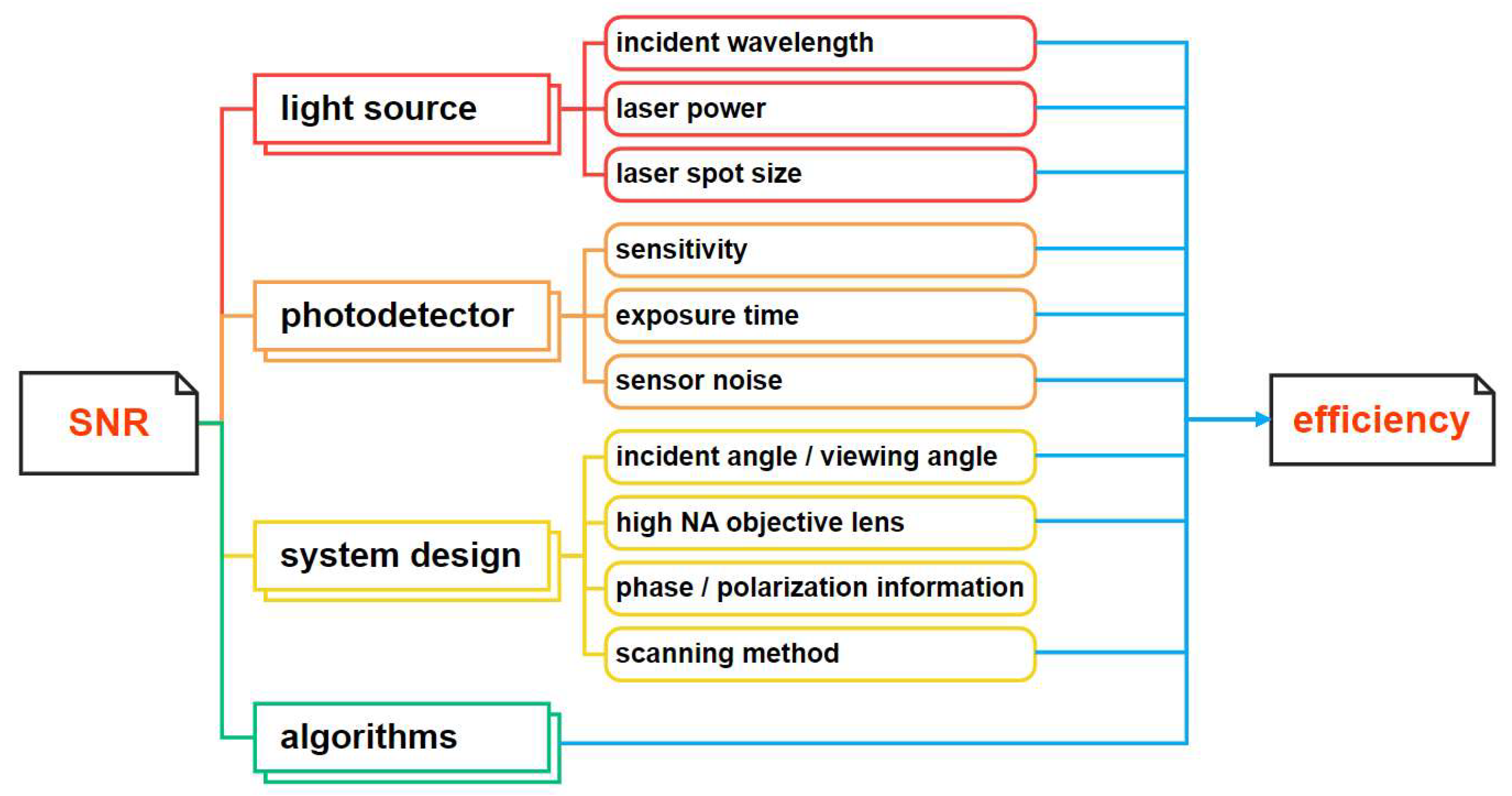
1. Introduction
2. Methodology
2.1. Dark-Field Scattering
2.2. Fundamental Aspects of TDI
3. Experimental Setup
4. Experimental Results and Discussions
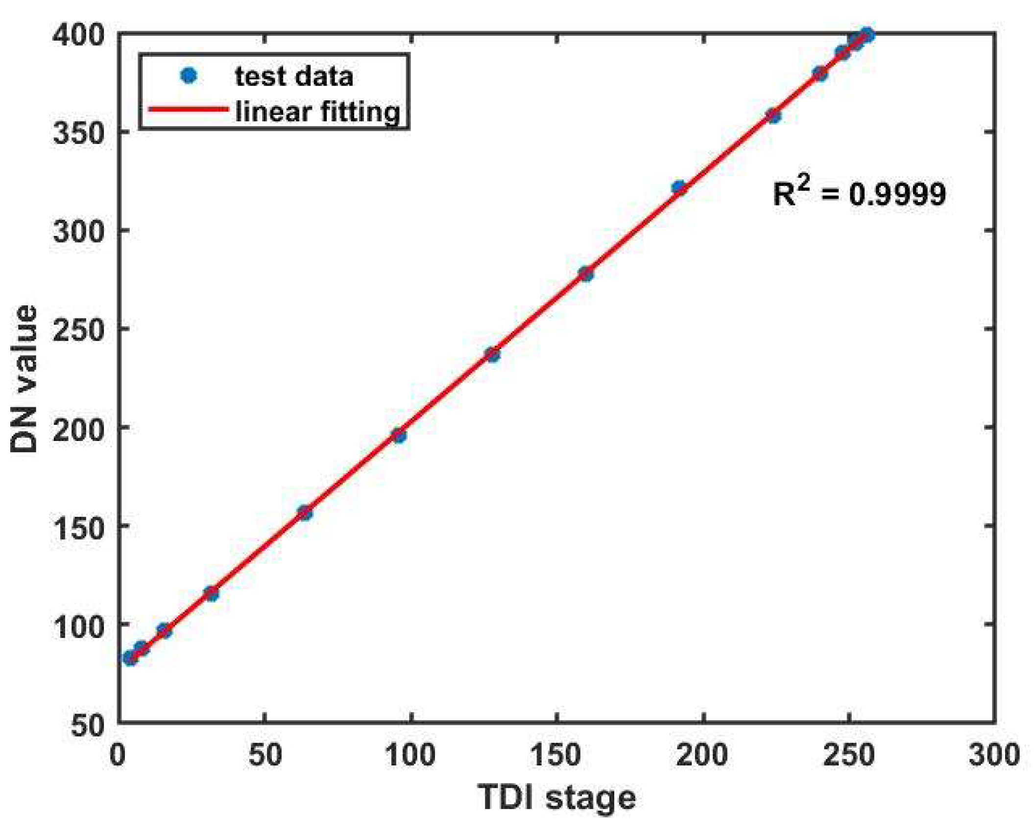
4.1. Linearity Assessment of the TDI Image Sensor
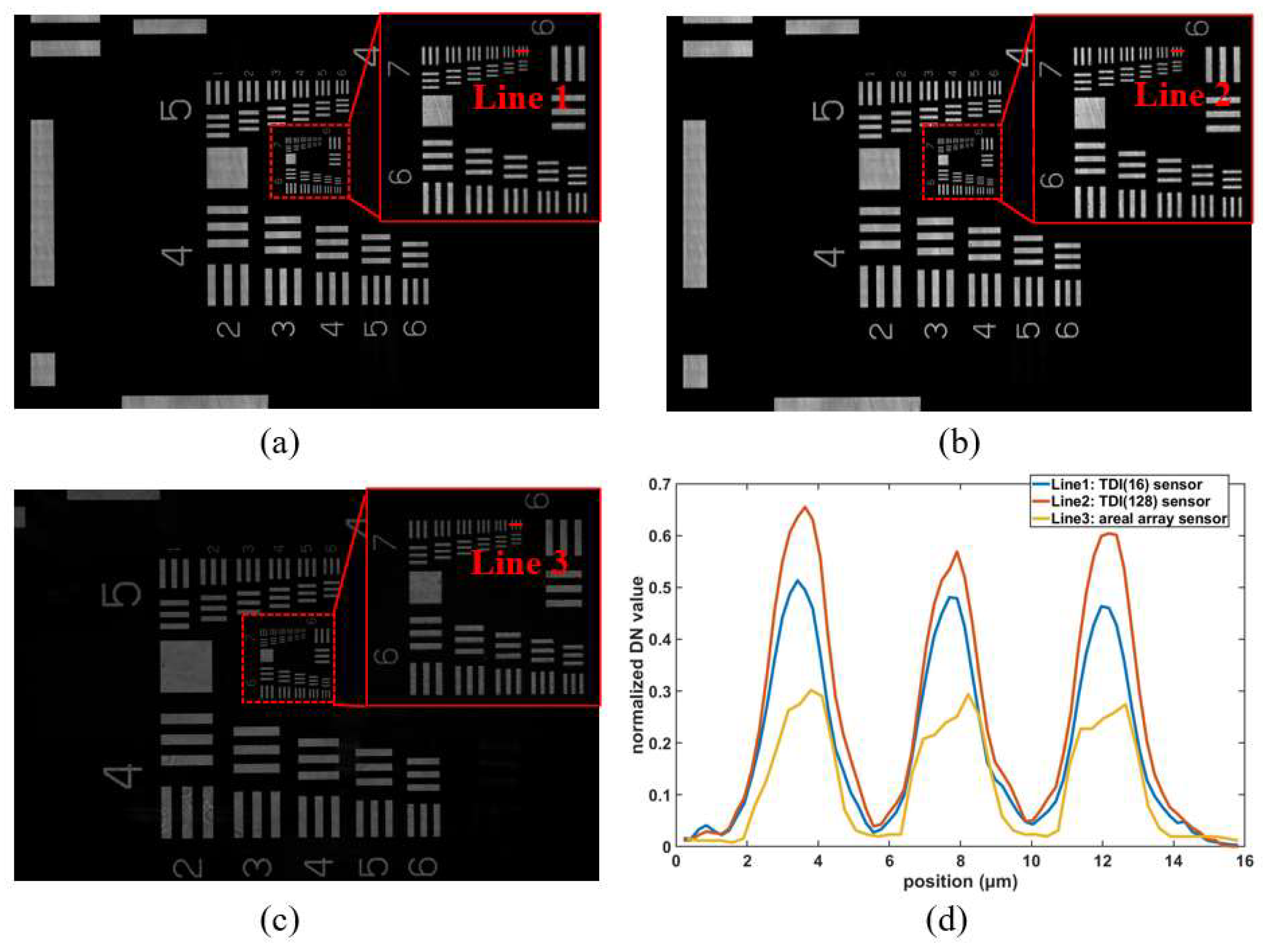
4.2. Resolution Target Imaging
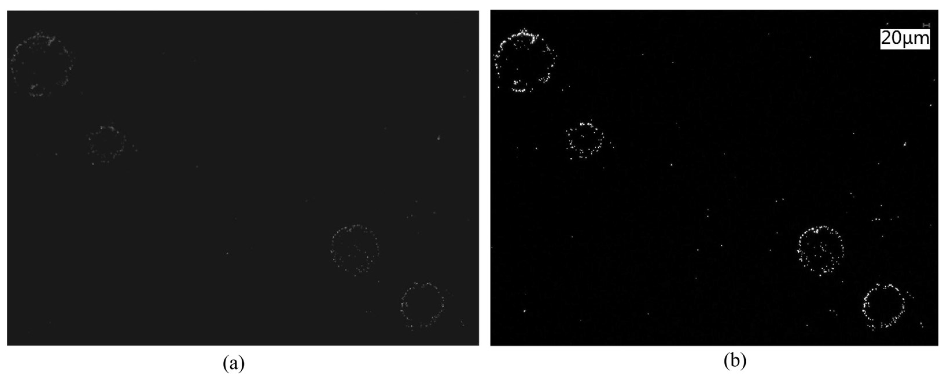
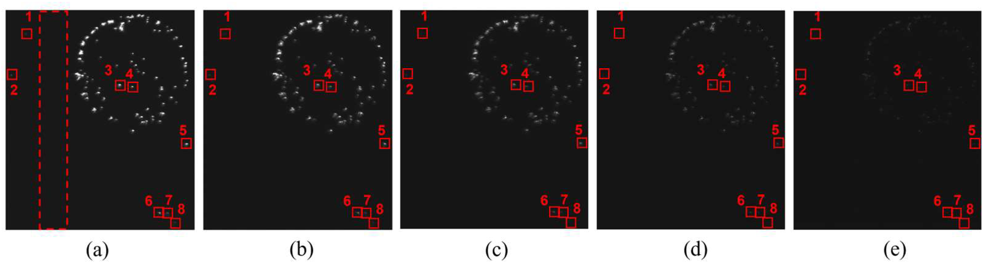
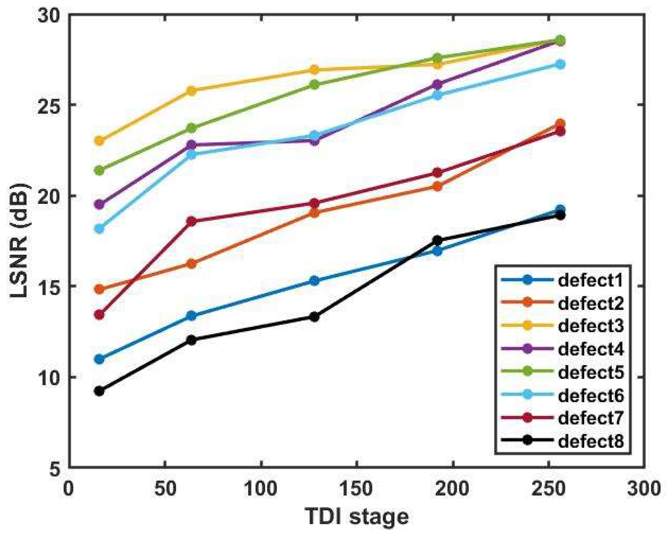
4.3. Particle Inspection on Non-Patterned Wafer
5. Conclusions
Author Contributions
Funding
Institutional Review Board Statement
Informed Consent Statement
Data Availability Statement
Conflicts of Interest
References
- Chen, X.; Wang, C.; Yang, T.; Liu, J.; Luo, C.; Liu, S. Inline Optical Measurement and Inspection for IC Manufacturing: State-of-the-Art, Challenges, and Perspectives. Laser Optoelectron. Prog. 2022, 59, 0922025. [Google Scholar] [CrossRef]
- Buengener, R. Defect Inspection Strategies for 14 Nm Semiconductor Technology. In Proceedings of the Instrumentation, Metrology, and Standards for Nanomanufacturing, Optics, and Semiconductors VI, San Diego, CA, USA, 11 October 2012; p. 846607. [Google Scholar]
- Oberai, A.; Yuan, J.-S. Smart E-Beam for Defect Identification & Analysis in the Nanoscale Technology Nodes: Technical Perspectives. Electronics 2017, 6, 87. [Google Scholar] [CrossRef]
- Nakagaki, R.; Honda, T.; Nakamae, K. Automatic Recognition of Defect Areas on a Semiconductor Wafer Using Multiple Scanning Electron Microscope Images. Meas. Sci. Technol. 2009, 20, 075503. [Google Scholar] [CrossRef]
- Hussain, D.; Ahmad, K.; Song, J.; Xie, H. Advances in the Atomic Force Microscopy for Critical Dimension Metrology. Meas. Sci. Technol. 2017, 28, 012001. [Google Scholar] [CrossRef]
- Li, M.; Hou, X.; Zhao, W.; Wang, H.; Li; Hu, X.; Zhao, Y.; Zhou, Y. Current situation and development trend of aspheric optical surface defect detection technology (invited). Infrared Laser Eng. 2022, 51, 11–30. [Google Scholar]
- Kim, C.-S.; Yoo, H. Three-Dimensional Confocal Reflectance Microscopy for Surface Metrology. Meas. Sci. Technol. 2021, 32, 102002. [Google Scholar] [CrossRef]
- Guldi, R.L. In-Line Defect Reduction from a Historical Perspective and Its Implications for Future Integrated Circuit Manufacturing. IEEE Trans. Semicond. Manuf. 2004, 17, 629–640. [Google Scholar] [CrossRef]
- Nakamae, K. Electron Microscopy in Semiconductor Inspection. Meas. Sci. Technol. 2021, 32, 052003. [Google Scholar] [CrossRef]
- Zhu, J.; Liu, J.; Xu, T.; Yuan, S.; Zhang, Z.; Jiang, H.; Gu, H.; Zhou, R.; Liu, S. Optical Wafer Defect Inspection at the 10 Nm Technology Node and Beyond. Int. J. Extreme Manuf. 2022, 4, 032001. [Google Scholar] [CrossRef]
- Zhou, R.; Edwards, C.; Popescu, G.; Goddard, L.L. 9 nm Node Wafer Defect Inspection Using Visible Light. In Proceedings of the Metrology, Inspection, and Process Control for Microlithography XXVIII, San Jose, CA, USA, 2 April 2014; Volume 9050, pp. 332–338. [Google Scholar]
- Kim, G.B. A Structured Mechanism Development and Experimental Parameter Selection of Laser Scattering for the Surface Inspection of Flat-Panel Glasses. Int. J. Prod. Res. 2010, 48, 3911–3923. [Google Scholar] [CrossRef]
- Zhou, R.; Edwards, C.; Arbabi, A.; Popescu, G.; Goddard, L.L. Detecting 20 Nm Wide Defects in Large Area Nanopatterns Using Optical Interferometric Microscopy. Nano Lett. 2013, 13, 3716–3721. [Google Scholar] [CrossRef] [PubMed]
- Chen, X.; Gu, H.; Liu, J.; Chen, C.; Liu, S. Advanced Mueller Matrix Ellipsometry: Instrumentation and Emerging Applications. Sci. China Technol. Sci. 2022, 65, 2007–2030. [Google Scholar] [CrossRef]
- Dong, J.; Chang, K.; Tian, Z.; Zhang, T.; Lang, X.; Zhang, Y.; Lu, R.; Xie, X. Development of a Confocal Line-Scan Laser Scattering Probe for Dark-Field Surface Defects Detection of Transmissive Optics. Rev. Sci. Instrum. 2022, 93, 083703. [Google Scholar] [CrossRef] [PubMed]
- Nolot, E.; Arrazat, B.; Favier, S.; Borde, Y.; Damlencourt, J.F.; Vincent, B.; Kermarrec, O.; Carron, V.; Nemouchi, F.; Vandelle, P.; et al. Laser Scattering: A Fast, Sensitive, In-Line Technique for Advanced Process Development and Monitoring. In Proceedings of the 2007 International Conference on Frontiers of Characterization and Metrology, Gaithersburg, MD, USA, 27–29 March 2007; AIP: Gaithersburg, MD, USA, 2007; Volume 931, pp. 116–120. [Google Scholar]
- Dong, J. Line-Scanning Laser Scattering System for Fast Defect Inspection of a Large Aperture Surface. Appl. Opt. 2017, 56, 7089. [Google Scholar] [CrossRef] [PubMed]
- Liu, C.; Xu, S.; Liu, Y.; Xiao, Z. Aperture Design for a Dark-Field Wafer Defect Inspection System. Appl. Opt. 2021, 60, 10830. [Google Scholar] [CrossRef] [PubMed]
- Liu, D.; Yang, Y.; Wang, L.; Zhuo, Y.; Lu, C.; Yang, L.; Li, R. Microscopic Scattering Imaging Measurement and Digital Evaluation System of Defects for Fine Optical Surface. Opt. Commun. 2007, 278, 240–246. [Google Scholar] [CrossRef]
- Liu, D.; Wang, S.; Cao, P.; Li, L.; Cheng, Z.; Gao, X.; Yang, Y. Dark-Field Microscopic Image Stitching Method for Surface Defects Evaluation of Large Fine Optics. Opt. Express 2013, 21, 5974. [Google Scholar] [CrossRef] [PubMed]
- Zhang, Y.; Yang, Y.; Li, C.; Wu, F.; Chai, H.; Yan, K.; Zhou, L.; Li, Y.; Liu, D.; Bai, J.; et al. Defects Evaluation System for Spherical Optical Surfaces Based on Microscopic Scattering Dark-Field Imaging Method. Appl. Opt. 2016, 55, 6162–6171. [Google Scholar] [CrossRef]
- Wang, S.; Liu, D.; Yang, Y.; Chen, X.; Cao, P.; Li, L.; Yan, L.; Cheng, Z.; Shen, Y. Distortion Correction in Surface Defects Evaluating System of Large Fine Optics. Opt. Commun. 2014, 312, 110–116. [Google Scholar] [CrossRef]
- Li, C.; Yang, Y.; Chai, H.; Zhang, Y.; Wu, F.; Zhou, L.; Yan, K.; Bai, J.; Shen, Y.; Xu, Q.; et al. Dark-Field Detection Method of Shallow Scratches on the Super-Smooth Optical Surface Based on the Technology of Adaptive Smoothing and Morphological Differencing. Chin. Opt. Lett. 2017, 15, 081202. [Google Scholar] [CrossRef]
- Kolenov, D.; Pereira, S.F. Machine Learning Techniques Applied for the Detection of Nanoparticles on Surfaces Using Coherent Fourier Scatterometry. Opt. Express 2020, 28, 19163. [Google Scholar] [CrossRef] [PubMed]
- Fan, S.-K.S.; Hsu, C.-Y.; Jen, C.-H.; Chen, K.-L.; Juan, L.-T. Defective Wafer Detection Using a Denoising Autoencoder for Semiconductor Manufacturing Processes. Adv. Eng. Inform. 2020, 46, 101166. [Google Scholar] [CrossRef]
- Liu, J.; Zhao, H.; Wu, Q.; Feng, X.; Zhao, X.; Zhang, Z.; Zhang, C.; Huang, T.; Zhu, J.; Liu, S. Patterned Wafer Defect Inspection at Advanced Technology Nodes. Laser Optoelectron. Prog. 2023, 60, 0312003. [Google Scholar] [CrossRef]
- Bian, Z.; Guo, C.; Jiang, S.; Zhu, J.; Wang, R.; Song, P.; Zhang, Z.; Hoshino, K.; Zheng, G. Autofocusing Technologies for Whole Slide Imaging and Automated Microscopy. J. Biophotonics 2020, 13, e202000227. [Google Scholar] [CrossRef] [PubMed]
- Zhong, Q.; Li, A.; Jin, R.; Zhang, D.; Li, X.; Jia, X.; Ding, Z.; Luo, P.; Zhou, C.; Jiang, C.; et al. High-Definition Imaging Using Line-Illumination Modulation Microscopy. Nat. Methods 2021, 18, 309–315. [Google Scholar] [CrossRef] [PubMed]
- Schacht, P.; Johnson, S.B.; Santi, P.A. Implementation of a Continuous Scanning Procedure and a Line Scan Camera for Thin-Sheet Laser Imaging Microscopy. Biomed. Opt. Express 2010, 1, 598. [Google Scholar] [CrossRef]
- Li, L.; Liu, D.; Cao, P.; Xie, S.; Li, Y.; Chen, Y.; Yang, Y. Automated Discrimination between Digs and Dust Particles on Optical Surfaces with Dark-Field Scattering Microscopy. Appl. Opt. 2014, 53, 5131. [Google Scholar] [CrossRef]
- Sun, H.; Wang, S.; Hu, X.; Liu, H.; Zhou, X.; Huang, J.; Cheng, X.; Sun, F.; Liu, Y.; Liu, D. Detection of Surface Defects and Subsurface Defects of Polished Optics with Multisensor Image Fusion. PhotoniX 2022, 3, 6. [Google Scholar] [CrossRef]
- Neubecker, R.; Hon, J.E. Automatic Inspection for Surface Imperfections: Requirements, Potentials and Limits. In Proceedings of the Third European Seminar on Precision Optics Manufacturing, Teisnach, Germany, 30 June 2016; p. 1000907. [Google Scholar]
- Germer, T.A. Angular Dependence and Polarization of Out-of-Plane Optical Scattering from Particulate Contamination, Subsurface Defects, and Surface Microroughness. Appl. Opt. 1997, 36, 8798. [Google Scholar] [CrossRef]


| Scanning Mode | Advantages | Disadvantages |
|---|---|---|
| point scanning | high speed | noise-sensitive, 1D signal |
| areal scanning | low noise | low speed, image stitching |
| Parameter | Parameter Value |
|---|---|
| photosensitive area | 45.36 mm × 1.28 mm |
| pixel size | 5 μm × 5 μm |
| number of active pixels | 9072 × 256 |
| max line frequency | 608 kHz |
| ADC depth | 10 bits |
| available TDI stages | 4, 8, 16, 32, 64, 128, 160, 192, 224, 240, 248, 252, 256 |
| TDI Stage | 16 | 64 | 128 | 192 | 256 |
|---|---|---|---|---|---|
| means (DN) | 79.5188 | 81.5049 | 86.6343 | 91.3814 | 96.2994 |
| standard deviation (DN) | 0.8236 | 0.8825 | 1.0533 | 1.1870 | 1.2856 |
| TDI Stage | 16 | 64 | 128 | 192 | 256 |
|---|---|---|---|---|---|
| standard deviation (DN) | 0.3937 | 0.4419 | 0.5527 | 0.6279 | 0.6853 |
| Specification | TDI-DFSM Parameter | Application Parameter |
|---|---|---|
| laser wavelength | 405 nm | 248 nm or 193 nm |
| laser power | 100 mW | several/tens of watts |
| resolution | 0.823 μm | 0.392 μm |
| detection sensitivity | 0.5 μm | <0.392 μm |
| line frequency | 23,400 Hz | 608 kHz |
| scanning speed | 5 mm/s | 129 mm/s |
| imaging efficiency | 10 mm2/s | 249 mm2/s |
| scanning time for 8-inch wafer | 1.12 h | 3 min |
Disclaimer/Publisher’s Note: The statements, opinions and data contained in all publications are solely those of the individual author(s) and contributor(s) and not of MDPI and/or the editor(s). MDPI and/or the editor(s) disclaim responsibility for any injury to people or property resulting from any ideas, methods, instructions or products referred to in the content. |
© 2024 by the authors. Licensee MDPI, Basel, Switzerland. This article is an open access article distributed under the terms and conditions of the Creative Commons Attribution (CC BY) license (https://creativecommons.org/licenses/by/4.0/).
Share and Cite
Yu, F.; Xu, M.; Wang, J.; Zhang, X.; Tang, X. Balancing the Efficiency and Sensitivity of Defect Inspection of Non-Patterned Wafers with TDI-Based Dark-Field Scattering Microscopy. Sensors 2024, 24, 1622. https://doi.org/10.3390/s24051622
Yu F, Xu M, Wang J, Zhang X, Tang X. Balancing the Efficiency and Sensitivity of Defect Inspection of Non-Patterned Wafers with TDI-Based Dark-Field Scattering Microscopy. Sensors. 2024; 24(5):1622. https://doi.org/10.3390/s24051622
Chicago/Turabian StyleYu, Fei, Min Xu, Junhua Wang, Xiangchao Zhang, and Xinlan Tang. 2024. "Balancing the Efficiency and Sensitivity of Defect Inspection of Non-Patterned Wafers with TDI-Based Dark-Field Scattering Microscopy" Sensors 24, no. 5: 1622. https://doi.org/10.3390/s24051622
APA StyleYu, F., Xu, M., Wang, J., Zhang, X., & Tang, X. (2024). Balancing the Efficiency and Sensitivity of Defect Inspection of Non-Patterned Wafers with TDI-Based Dark-Field Scattering Microscopy. Sensors, 24(5), 1622. https://doi.org/10.3390/s24051622