
A gm/ID-Based Low-Power LNA for Ka-Band Applications

 , , and
Abstract
1. Introduction
2. Design Procedure
- Generates DC sweeps for all corners. These corners are generated by considering all possible combinations of process, temperature, and noise variations and depend on the PDK used. In this case, the combinations include typical (T), slow (S), and fast (F) devices with −40 °C, 16 °C, 125 °C and high-, nominal-, and low-noise corners.
- Maps the FET’s operating point parameters into the desired output variables to build a multidimensional MATLAB matrix from the Cadence database results.
- Generates the Spectre simulation netlists with the desired geometries and sweeps.
- Sequentially runs all the previously generated simulations.
- Generates a .mat file with the multidimensional data for each corner as a result.
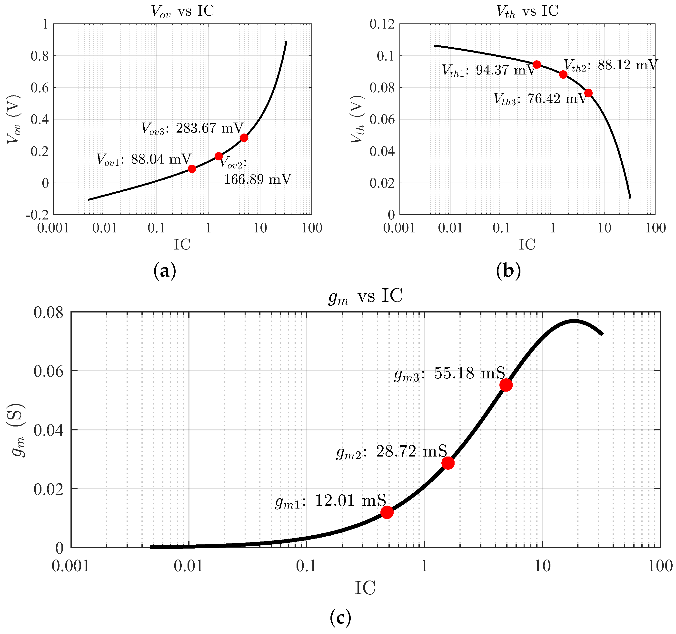
3. MOSFET Characterization and Simulation Results
4. Conclusions
Author Contributions
Funding
Institutional Review Board Statement
Informed Consent Statement
Data Availability Statement
Conflicts of Interest
Abbreviations
| Gate-Source Capacitance | |
| Gate-Drain Capacitance | |
| Source-Drain Capacitance | |
| Drain-Bulk Capacitance | |
| CMOS | Complementary Metal Oxide Semiconductor |
| IC | Inversion coefficient |
| Drain current | |
| Gate-Drain Current | |
| Gate-Source Current | |
| IRL | Input Return Loss |
| FB | Floating-Body |
| FoM | Figure of Merit |
| Drain-Source Transconductance | |
| Regular Transconductance | |
| Gate-Bulk Transconductance | |
| LNA | Low-Noise Amplifier |
| MMIC | Monolithic Microwave Integrated Circuit |
| MW | Microwave |
| NF | Noise figure |
| ORL | Output Return Loss |
| PDK | Process Design Kit |
| RF | Radiofrequency |
| RFIC | RF Integrated Circuit |
| UWB | Ultrawide Band |
| VDS | Drain-Source Voltage |
| VGA | Variable Gain Amplifier |
| VGS | Gate-Source Voltage |
| VTH | Threshold Voltage |
| SATCOM | Satellite Communications |
| SOI | Silicon-on-insulator |
| STH | Thermal Noise coefficient |
| SFL | Flicker Noise Coefficient |
| Unit Finger Width |
References
- Razavi, B. RF Microelectronics, 2nd ed.; Prentice Hall Communications Engineering and Emerging Technologies Series; Prentice Hall Press: Hoboken, NJ, USA, 2011; ISBN 0137134738. [Google Scholar]
- Lee, T.H. The Design of CMOS Radio-Frequency Integrated Circuits; Cambridge University Press: Cambridge, UK, 2004; ISBN 0521835399. [Google Scholar]
- Yeom, K.-W. Microwave Circuit Design: A Practical Approach Using ADS; Prentice Hall: Hoboken, NJ, USA, 2015; ISBN 0134085825. [Google Scholar]
- Piccinni, G.; Avitabile, G.; Coviello, G.; Talarico, C. Distributed amplifier design for UWB positioning systems using the gm over id methodology. In Proceedings of the 2016 13th International Conference on Synthesis, Modeling, Analysis and Simulation Methods and Applications to Circuit Design (SMACD), Lisbon, Portugal, 27–30 June 2016; pp. 1–4. [Google Scholar] [CrossRef]
- Elmeligy, K.; Omran, H. Fast Design Space Exploration and Multi-Objective Optimization of Wide-Band Noise-Canceling LNAs. Electronics 2022, 11, 816. [Google Scholar] [CrossRef]
- Piccinni, G.; Avitabile, G.; Coviello, G.; Talarico, C. Gm over ID design for UWB distributed amplifier. In Proceedings of the 2016 IEEE 59th International Midwest Symposium on Circuits and Systems (MWSCAS), Abu Dhabi, United Arab Emirates, 16–19 October 2016; pp. 1–4. [Google Scholar] [CrossRef]
- Belostotski, L.; Jagtap, S. Down with Noise: An Introduction to a Low-Noise Amplifier Survey. IEEE Solid-State Circuits Mag. 2020, 12, 23–29. [Google Scholar] [CrossRef]
- Khavari, A.F.; Mafinezhad, K. A New UWB LNA with 15 dB Gain in 90 nm CMOS with Current Reuse Topology. In Proceedings of the Electrical Engineering (ICEE), Iranian Conference, Mashhad, Iran, 8–10 May 2018; pp. 184–189. [Google Scholar] [CrossRef]
- Tripathy, D.; Nayak, D.; Biswal, S.M.; Swain, S.K.; Baral, B.; Das, S.K. A Low Power LNA using Current Reused Technique for UWB Application. In Proceedings of the 2019 Devices for Integrated Circuit (DevIC), Kalyani, India, 23–24 March 2019; pp. 310–313. [Google Scholar] [CrossRef]
- Chen, W.-W.; Yang, S.-D.; Cheng, K.-W. A 1.2 V 490 μW Sub-GHz UWB CMOS LNA with Current Reuse Negative Feedback. In Proceedings of the 2018 IEEE International Symposium on Circuits and Systems (ISCAS), Florence, Italy, 27–30 May 2018; pp. 1–4. [Google Scholar] [CrossRef]
- Jespers, P.G.A. The gm/ID Methodology, a Sizing Tool for Low-Voltage Analog CMOS Circuits; Springer Science and Business Media: Berlin/Heidelberg, Germany, 2009; ISBN 0387471014. [Google Scholar]
- Jespers, P.G.A. Boris Murmann, Systematic Design of Analog CMOS Circuits; Cambridge University Press: Cambridge, UK, 2017; ISBN 1107192250. [Google Scholar]
- Youssef, A.A.; Murmann, B.; Omran, H. Analog IC Design Using Precomputed Lookup Tables: Challenges and Solutions. IEEE Access 2020, 8, 134640–134652. [Google Scholar] [CrossRef]
- Enz, C.C.; Chicco, F.; Pezzotta, A. Nanoscale MOSFET Modeling: Part 2: Using the Inversion Coefficient as the Primary Design Parameter. IEEE Solid-State Circuits Mag. 2017, 9, 73–81. [Google Scholar] [CrossRef]
- Aueamnuay, C.; Kayyil, A.V.; Liu, J.; Thota, N.B.; Allstot, D.J. Gm/ID Design Considerations for Subthreshold-Based CMOS Two-Stage Operational Amplifiers. In Proceedings of the 2020 IEEE International Symposium on Circuits and Systems (ISCAS), Seville, Spain, 12–14 October 2020; pp. 1–5. [Google Scholar] [CrossRef]
- Hesham, B.; Hasaneen, E.-S.; Hamed, H.F.A. Design Procedure for Two-Stage CMOS Opamp using gm/ID design Methodology in 16 nm FinFET Technology. In Proceedings of the 2019 31st International Conference on Microelectronics (ICM), Cairo, Egypt, 15–18 December 2019; pp. 325–329. [Google Scholar] [CrossRef]
- Liu, J.; Lauga-Larroze, E.; Subias, S.; Fournier, J.-M.; Bourdel, S.; Galup, C.; Hameau, F. A Methodology for the Design of Capacitive Feedback LNAs based on the gm/ID Characteristic. In Proceedings of the 2018 16th IEEE International New Circuits and Systems Conference (NEWCAS), Montreal, QC, Canada, 24–27 June 2018; pp. 178–181. [Google Scholar] [CrossRef]
- Xie, Q.; Li, Z.; Shi, G. Design Space Exploration of Multi-Stage Op Amps by Symbolic Modeling and gm/ID Sampling. In Proceedings of the 2023 International Symposium of Electronics Design Automation (ISEDA), Nanjing, China, 8–11 May 2023; pp. 40–45. [Google Scholar] [CrossRef]
- Kumar, T.B.; Sharma, G.K.; Johar, A.K.; Gupta, D.; Kar, S.K.; Boolchandani, D. Design Automation of 5-T OTA using gm/ID methodology. In Proceedings of the 2019 IEEE Conference on Information and Communication Technology, Allahabad, India, 6–8 December 2019; pp. 1–5. [Google Scholar] [CrossRef]
- Castagnola, J.L.; García-Vázquez, H.; Dualibe, F.C. Design and optimisation of a cascode low noise amplifier (LNA) using MOST scattering parameters and gm/ID ratio. In Proceedings of the 2018 IEEE 9th Latin American Symposium on Circuits and Systems (LASCAS), Puerto Vallarta, Mexico, 25–28 February 2018; pp. 1–4. [Google Scholar] [CrossRef]
- Fiorelli, R.; Núñez, J.; Silveira, F. All-inversion region gm/ID methodology for RF circuits in FinFET technologies. In Proceedings of the 2018 16th IEEE International New Circuits and Systems Conference (NEWCAS), Montreal, QC, Canada, 24–27 June 2018; pp. 170–173. [Google Scholar] [CrossRef]
- Chung, J.; Iliadis, A.A. Modeling a High Linearity, Low Noise Gilbert Cell Mixer using Three Optimization Techniques. In Proceedings of the 2020 IEEE 63rd International Midwest Symposium on Circuits and Systems (MWSCAS), Springfield, MA, USA, 9–12 August 2020; pp. 790–793. [Google Scholar] [CrossRef]
- Piccinni, G.; Avitabile, G.; Coviello, G.; Talarico, C. Gilbert cell mixer design based on a novel systematic approach for nanoscale technologies. In Proceedings of the 2017 IEEE 18th Wireless and Microwave Technology Conference (WAMICON), Cocoa Beach, FL, USA, 24–25 April 2017; pp. 1–4. [Google Scholar] [CrossRef]
- Rudenko, T.; Nazarov, A.N.; Lysenko, V.S. The advancement of silicon-on-insulator (SOI) devices and their basic properties. Semicond. Phys. Quantum Electron. Optoelectron. 2020, 23, 227–252. [Google Scholar] [CrossRef]
- Wang, Y.; Cui, J.; Zhang, R. A K to Ka Band Single-ended to Balanced Ultra-wideband LNA in 45nm CMOS SOI. In Proceedings of the 2019 IEEE International Symposium on Radio-Frequency Integration Technology (RFIT), Nanjing, China, 28–30 August 2019; pp. 1–3. [Google Scholar] [CrossRef]
- Cuadrado-Calle, D.; George, D.; Fuller, G. A GaAs Ka-band (26–36 GHz) LNA for radio astronomy. In Proceedings of the 2014 IEEE International Microwave and RF Conference (IMaRC), Bangalore, India, 15–17 December 2014; pp. 301–303. [Google Scholar] [CrossRef]
- Cetin, T.; Onol, C.; Selcuk, G. A Ka-Band Front-End in 100nm GaAs Process for In-Band Full Duplex Communications. In Proceedings of the IEEE EUROCON 2019—18th International Conference on Smart Technologies, Novi Sad, Serbia, 1–4 July 2019; pp. 1–4. [Google Scholar] [CrossRef]
- Dilshad, U.; Chen, C.; Altaf, A.; Miao, J. An Ultra-Broadband K Ka-Band (17–40 GHz) LNA MMIC in 0.15 μm GaAs pHEMT. In Proceedings of the 2019 International Conference on Microwave and Millimeter Wave Technology (ICMMT), Guangzhou, China, 19–22 May 2019; pp. 1–3. [Google Scholar] [CrossRef]
- Li, C.; El-Aassar, O.; Kumar, A.; Boenke, M.; Rebeiz, G.M. LNA Design with CMOS SOI Process-l.4dB NF K/Ka band LNA. In Proceedings of the 2018 IEEE/MTT-S International Microwave Symposium—IMS, Philadelphia, PA, USA, 10–15 June 2018; pp. 1484–1486. [Google Scholar] [CrossRef]
- Dahlman, E.; Parkvall, S.; Sköld, J. 5G NR: The Next Generation Wireless Access Technology, 1st ed.; Academic Press Cambridge: Cambridge, MA, USA, 2018. [Google Scholar] [CrossRef]
- Castagnola, J.L.; Dualibe, F.C.; Laprovitta, A.M.; García-Vázquez, H. A Novel Design and Optimization Approach for Low Noise Amplifiers (LNA) Based on MOST Scattering Parameters and the gm/ID Ratio. Electronics 2020, 9, 785. [Google Scholar] [CrossRef]
- Kong, S.; Lee, H.-D.; Jang, S.; Park, J.; Kim, K.-S.; Lee, K.-C. A 28-GHz CMOS LNA with Stability-Enhanced Gm-Boosting Technique Using Transformers. In Proceedings of the 2019 IEEE Radio Frequency Integrated Circuits Symposium (RFIC), Boston, MA, USA, 2–4 June 2019; pp. 7–10. [Google Scholar] [CrossRef]
- Elkholy, M.; Shakib, S.; Dunworth, J.; Aparin, V.; Entesari, K. A Wideband Variable Gain LNA with High OIP3 for 5G Using 40-nm Bulk CMOS. IEEE Microw. Wirel. Compon. Lett. 2018, 28, 64–66. [Google Scholar] [CrossRef]
- Qin, P.; Xue, Q. Compact Wideband LNA with Gain and Input Matching Bandwidth Extensions by Transformer. IEEE Microw. Wirel. Compon. Lett. 2017, 27, 657–659. [Google Scholar] [CrossRef]
- Lee, S.; Park, J.; Hong, S. A Ka-Band Phase-Compensated Variable-Gain CMOS Low-Noise Amplifier. IEEE Microw. Wirel. Compon. Lett. 2019, 29, 131–133. [Google Scholar] [CrossRef]
- Nawaz, A.A.; Albrecht, J.D.; Ulusoy, A.Ç. A Ka/V Band-Switchable LNA with 2.8/3.4 dB Noise Figure. IEEE Microw. Wirel. Compon. Lett. 2019, 29, 662–664. [Google Scholar] [CrossRef]
- Enz, C.; Chicco, F.; Pezzotta, A. Nanoscale MOSFET Modeling: Part 1: The Simplified EKV Model for the Design of Low-Power Analog Circuits. IEEE Solid-State Circuits Mag. 2017, 9, 26–35. [Google Scholar] [CrossRef]
- El-Aassar, O.; Rebeiz, G.M. Design of Low-Power Sub-2.4 dB Mean NF 5G LNAs Using Forward Body Bias in 22 nm FDSOI. IEEE Trans. Microw. Theory Tech. 2020, 68, 4445–4454. [Google Scholar] [CrossRef]
- Sayginer, M.; Rebeiz, G.M. A W-Band LNA/Phase Shifter with 5-dB NF and 24-mW Power Consumption in 32-nm CMOS SOI. IEEE Trans. Microw. Theory Tech. 2018, 66, 1973–1982. [Google Scholar] [CrossRef]
- Gao, L.; Wagner, E.; Rebeiz, G.M. Design of E- and W-Band Low-Noise Amplifiers in 22-nm CMOS FD-SOI. IEEE Trans. Microw. Theory Tech. 2020, 68, 132–143. [Google Scholar] [CrossRef]
- Han, F.; Liu, X.; Wang, C.; Li, X.; Qi, Q.; Li, X.; Liu, Z. A multi-band LNA covering 17–38 GHz in 45 nm CMOS SOI. Electronics 2022, 11, 3255. [Google Scholar] [CrossRef]
- Chen, H.-H.; Tsai, Z.-M. Ka-/K-Band Frequency-Reconfigurable Single-Input Differential-Output Low-Noise Amplifier for 5G Applications. IEEE Microw. Wirel. Technol. Lett. 2023, 33, 1297–1300. [Google Scholar] [CrossRef]
- Hietanen, M.; Rusanen, J.; Aikio, J.P.; Tervo, N.; Rahkonen, T.; Pärssinen, A. Ka-Band TDD Front-End with Gate Shunt Switched Cascode LNA and Three-Stack PA on 22nm FDSOI CMOS Technology. In Proceedings of the 2020 50th European Microwave Conference (EuMC), Utrecht, The Netherlands, 12–14 January 2021; pp. 945–948. [Google Scholar] [CrossRef]
- Xu, X.; Schumann, S.; Ferschischi, A.; Finger, W.; Carta, C.; Ellinger, F. A 28 GHz and 38 GHz High-Gain Dual-Band LNA for 5G Wireless Systems in 22 nm FD-SOI CMOS. In Proceedings of the 2020 15th European Microwave Integrated Circuits Conference (EuMIC), Utrecht, The Netherlands, 10–15 January 2021; pp. 77–80. [Google Scholar]


| Parameter | = 0.48 | = 1.58 | = 4.92 |
|---|---|---|---|
| (mV) | 182 | 255 | 360 |
| (mV) | 94 | 88 | 76 |
| (mA) | 0.67 | 2.2 | 6.8 |
| (mS) | 12 | 28.7 | 55.2 |
| / (S/A) | 18 | 13 | 8 |
| W/L | 1.25 k | 1.25 k | 1.25 k |
| (dB) | 3.9 | 1.9 | 1.4 |
| (dB) | 8.6 | 14.2 | 17 |
| (mW) | 0.6 | 1.98 | 6.2 |
| (pH) | 180 | 135 | 104 |
| (pH) | 458 | 408 | 352 |
| (pH) | 500 | 500 | 500 |
| 5.7 | 4.2 | 2 |
| Reference | This Work | [41] | [42] | [43] | [44] | [29] |
|---|---|---|---|---|---|---|
| Tech. | 45 nm | 45 nm | 65 nm | 22 nm | 22 nm | 45 nm |
| SOI | SOI | CMOS | SOI | SOI | SOI | |
| BW (GHz) | 25.5–29.5 | 21–28 | 23.5–32.5 | 24–28 | 26.6–31.6 | 14–31 |
| Centre Freq. (GHz) | 27.5 | 24.5 | 27.5 | 26 | 29.1 | 22.5 |
| Supply (V) | 0.9 | 1 | 1 | 0.8 | 1.6 | 1.5 |
| Max Gain (dB) | 11.4 | 19.5 | 17.2 | 7 | 19.3 | 12.8 |
| Threshold Gain (dB) | 8.4 | 16.5 | 14.2 | 4 | 16.3 | 9.8 |
| NF (dB) | 3.5–3.8 | 4.7 | 2.8–3 | 5 | 5.2 | 1.4 |
| IRL (dB) | 12.7 | – | 25 | 6 | 10 | 10 |
| ORL (dB) | 10 | – | – | – | 10 | 10 |
| (mW) | 1.98 | 59 | 28.5 | 4.6 | 11.4 | 15 |
| Meas./Sim. | Sim | Meas. | Meas. | Meas. | Meas. | Meas. |
| 3.03 | 0.14 | 0.4 | 0.608 | 0.65 | 2.08 | |
| Core area (mm2) | 0.43 | 0.42 | 0.157 | 0.1 | 0.27 | 0.3 |
Disclaimer/Publisher’s Note: The statements, opinions and data contained in all publications are solely those of the individual author(s) and contributor(s) and not of MDPI and/or the editor(s). MDPI and/or the editor(s) disclaim responsibility for any injury to people or property resulting from any ideas, methods, instructions or products referred to in the content. |
© 2024 by the authors. Licensee MDPI, Basel, Switzerland. This article is an open access article distributed under the terms and conditions of the Creative Commons Attribution (CC BY) license (https://creativecommons.org/licenses/by/4.0/).
Share and Cite
Galante-Sempere, D.; Torres-Clarke, J.; del Pino, J.; Khemchandani, S.L. A gm/ID-Based Low-Power LNA for Ka-Band Applications. Sensors 2024, 24, 2646. https://doi.org/10.3390/s24082646
Galante-Sempere D, Torres-Clarke J, del Pino J, Khemchandani SL. A gm/ID-Based Low-Power LNA for Ka-Band Applications. Sensors. 2024; 24(8):2646. https://doi.org/10.3390/s24082646
Chicago/Turabian StyleGalante-Sempere, David, Jeffrey Torres-Clarke, Javier del Pino, and Sunil Lalchand Khemchandani. 2024. "A gm/ID-Based Low-Power LNA for Ka-Band Applications" Sensors 24, no. 8: 2646. https://doi.org/10.3390/s24082646
APA StyleGalante-Sempere, D., Torres-Clarke, J., del Pino, J., & Khemchandani, S. L. (2024). A gm/ID-Based Low-Power LNA for Ka-Band Applications. Sensors, 24(8), 2646. https://doi.org/10.3390/s24082646