1. Introduction
BC501A liquid scintillators are commonly used in nuclear physics applications. These detectors can simultaneously detect gamma radiation and neutrons. Upon the incidence of such a particle, ionization of the liquid occurs, and the de-excitation produces light in the ultraviolet and blue part of the visible spectrum. The light is then collected by a photomultiplier and converted into an electric pulse. The pulse shape produced by gamma photons differs from those produced by neutrons, and thus, an analysis of the pulse allows discrimination between both kinds of particles [
1,
2]. Guerrero et al. developed an improved method of digital pulse shape analysis (DPSA) [
3], which is based on the integration of two different ranges of the signal. The relationship between the charge collected in these two ranges allows for the identification of the pulse as produced by a gamma photon or by a neutron. The use of digital electronics and DPSA offers a more versatile solution than hardware-based analog-to-digital or charge-to-digital converters. There are different approaches to implementing the DPSA to discriminate neutrons and gamma, as summarized in [
4]. The majority of the solutions are based on digitizing the signals and implementing offline analysis applications using a computer. Additionally, there are emerging approaches that employ machine learning techniques for offline analysis and even real-time analysis using neural networks in data acquisition (DAQ) devices. In both cases, the amount of digitized data to be transferred to the computer can become a bottleneck when the number of channels and count rates in the detectors are large. As an alternative, the required calculations for the DPSA can be performed with reduced latencies by utilizing field-programmable gate arrays (FPGAs) and hardware process acceleration techniques, which are extensively used (see [
5]). This potentially enables real-time applications such as time-of-flight (ToF) measurements related to the measurement of neutron spectra in various types of nuclear physics experiments, especially under high count rate conditions [
6,
7]. However, the possibility of real-time analysis is highly dependent on the available FPGA resources and the algorithm’s complexity.
This paper proposes an FPGA-based hardware implementation for DPSA, using floating point operations, of signals from a BC501A liquid scintillator. The signals are digitalized at a rate of 1GS/s with 16-bit resolution for use in a real-time analysis system.
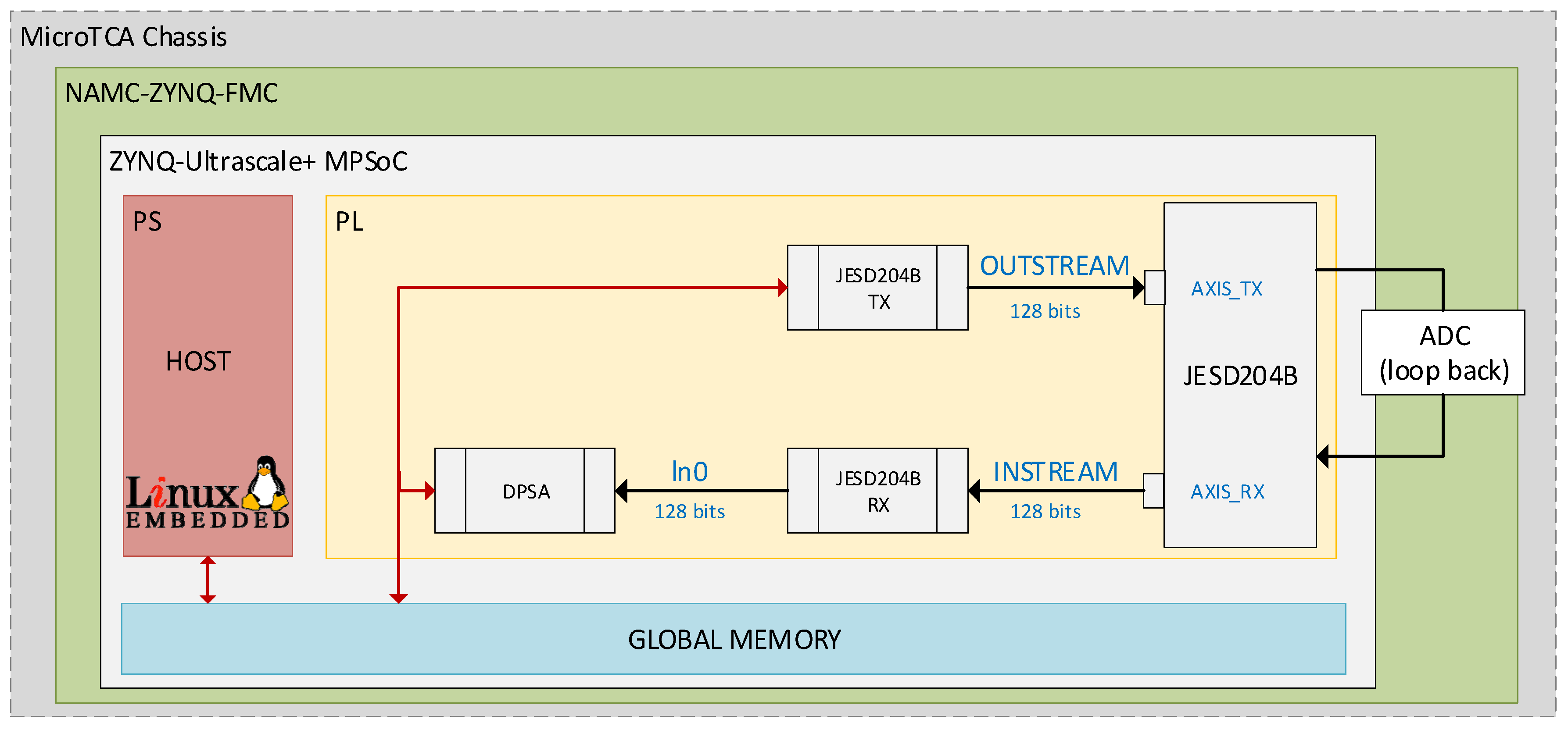
The system is based on a Micro Telecommunications Computing Architecture (MicroTCA) chassis [
8,
9,
10], which provides physical, mechanical, electrical, and thermal support for a NAMC-ZYNQ-FMC Advanced Mezzanine Card (AMC) [
11]. The NAMC-ZYNQ-FMC is a system-on-a-chip (SoC)-based AMC whose main component is a Xilinx ZYNQ Ultrascale + MP SoC [
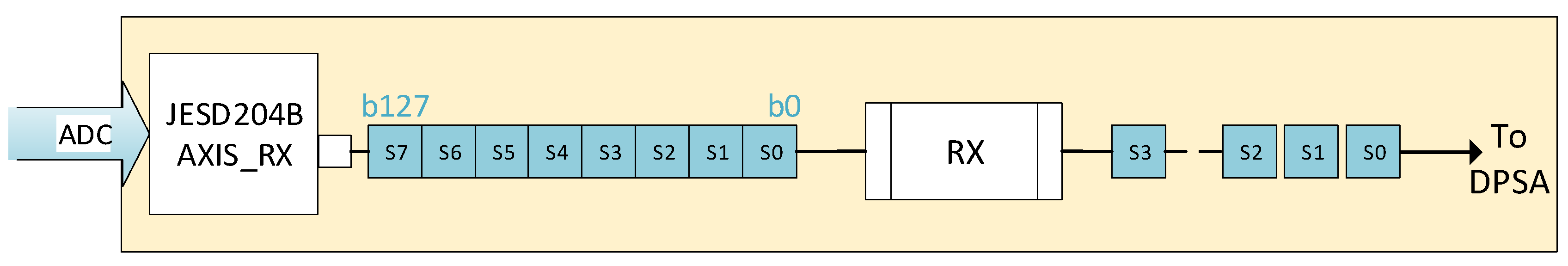
12]. The JESD204B standard [
13,
14] is implemented in the SoC programmable logic (PL) area to interface the digitizer and the DPSA application. This standard defines a serial interface that connects high-speed converters to logic devices such as FPGAs and Application Specific Integrated Circuits (ASIC). The JESD204B standard is implemented to connect the ADC directly to the processing hardware. Analog Devices provides an open-source intellectual property (IP) framework distributed under the GPL2 license to implement the JESD204 interface and the software to configure all the hardware elements [
15].
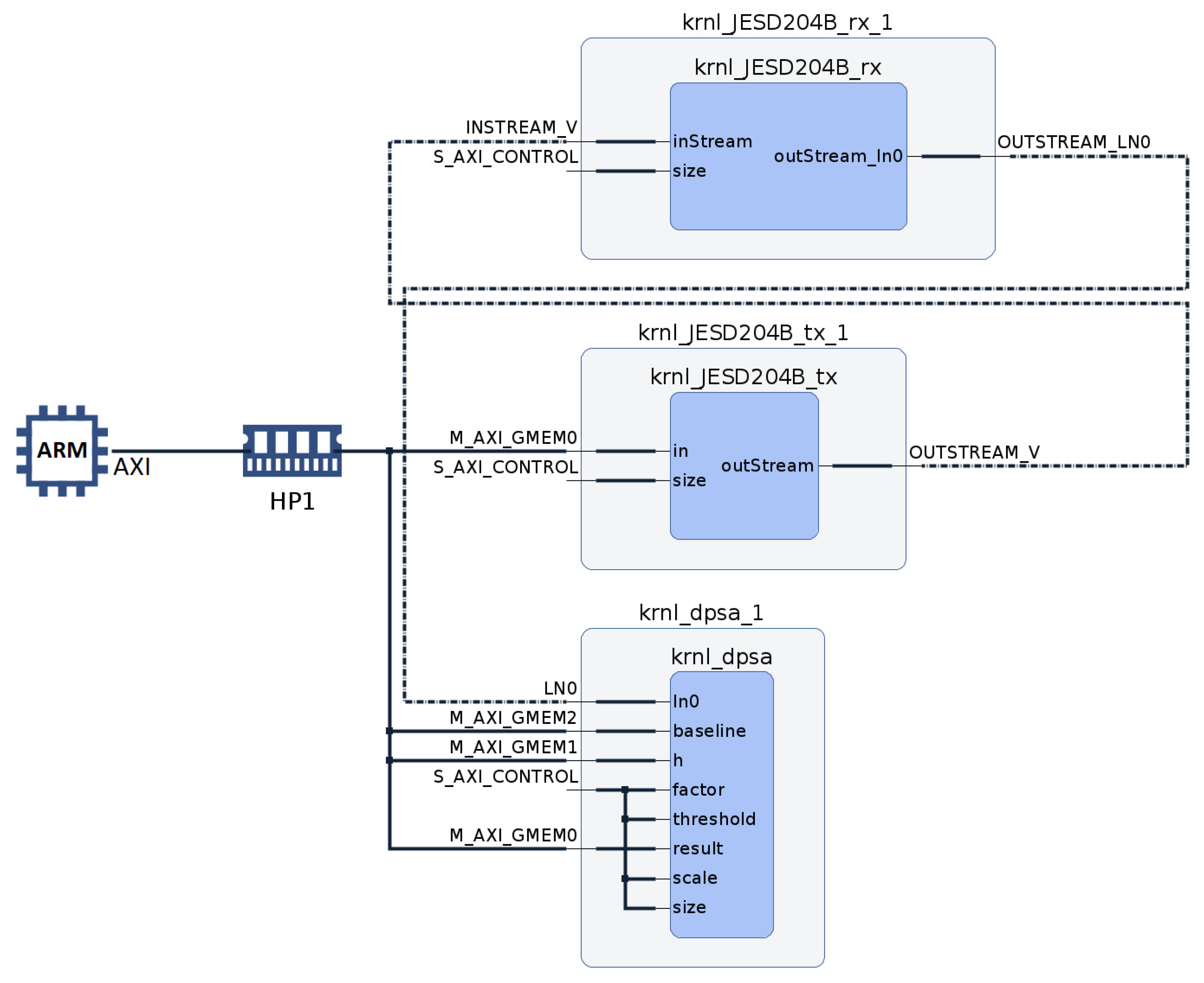
Figure 1 displays the stack of the hardware and software elements mentioned earlier. The bottom two layers of the stack show the MicroTCA chassis that supports the NAMC-ZYNQ-FMC board. The third layer from the bottom features the Xilinx ZYNQ Ultrascale + MP SoC, which integrates a high-performance ARM-based multicore multiprocessing system (PS) with ASIC-class PL.
The objective of this study is to evaluate the suitability and limitations of the MicroTCA platform for its use in a data acquisition system, with real-time analysis of the detector signals using a realistic pulse shape analysis algorithm.
Guerrero et al. [
3] state that the DPSA aims to extract the physically relevant parameters for the BC501A detector. The parameters include the time at which the pulse occurs, amplitude, and integrals over specific time intervals to determine the type of incident particle. The DPSA application layer, located at the top of the stack in
Figure 1, achieves this goal. The Xilinx ZYNQ Ultrascale + MP SoC within the processing system (PS) uses a Linux-embedded system to execute the DPSA application. This application coordinates kernel execution and reads the analysis results. The hardware kernels responsible for signal analysis and achieving the DPSA’s objectives are located in the SoC PL area. On the top layer of
Figure 1, the JESD204B interface is shown on the left. The DPSA kernels are also part of the application layer for the JESD204B standard.
Key contributions of the work are the use of floating-point-based hardware to achieve maximum accuracy in the estimation of the relevant parameters, the complete implementation of the DSPA algorithm using high-level synthesis (HLS) in a MicroTCA platform, and the measurement of the performance. A positive result can impact the design of the next generation of data acquisition systems to be used in nuclear physics experiments since it would combine the versatility of algorithms programmed in a high-level language with real-time analysis in high-count rate applications. To verify the implementation, nearly 400,000 signals digitalized from a BC501A and stored in a database were analyzed [
16].
4. Discussion
In the discussion section, three points should be considered: how the algorithm was optimized to reduce computational costs and achieve low latencies, what causes the accuracy errors presented in
Section 3.3, and whether the system can be considered a real-time system or not.
4.1. Algorithm Optimization
The algorithm has been optimized to create a high-speed processing system. It is unnecessary to process the entire signal since there is a significant amount of noise present around the pulses, which are the focal points of interest. This significantly increases computational cost, with 20 operations performed per sample in the FIR filter step. To address this issue, the function checks if the signal has passed the threshold that indicates a pulse has occurred while the input signal buffer is being filled from the input stream. Subsequent functions utilize this value to restrict the signal. The pulse width is a predetermined value that corresponds to the typical pulse width of this experiment. Therefore, the signal is also limited at the end of the pulse.
4.2. Accuracy Error
The issue arises from differences in implementation approaches. In the C++ implementation, the baseline is calculated twice. The entire signal is initially used except for the points whose variance exceeds a given value. This baseline is then used for subsequent calculations. A new value for the baseline is then calculated using only the contiguous sections of the pulse. This new value and the variance are presented as the result.
To reduce computation time and the FPGA resources used in the hardware implementation, the baseline is calculated only once using the contiguous sections of the pulse. Therefore, these baseline data and standard deviation in the table are precise. The calculated data is then used in the following functions.
Table 6 displays the mean and the standard deviation of error of the relevant parameters after processing the 398,957 signals, which exhibited negligible differences.
4.3. Real-Time System
Determining whether a system is real-time depends on the criteria used. It is important to note that the system’s latency is equivalent to that of the DPSA kernel, where the calculations are performed. Execution times for JESD204B TX and RX kernels are related to the global memory reading times of the signals. These signals are used solely to simulate signal generation and data acquisition behavior in conditions similar to the real experiment, facilitating prompt algorithm validation.
Table 2 in
Section 3.2 displays the execution times of the DPSA kernels. The maximum value is 134 µs, and the average is 99 µs, indicating stable values.
4.4. Potential Application
This work was aimed at potential applications in the nuclear science field, where data acquisition systems (DAQs) have traditionally relied on analog electronics. However, the possibility of directly digitizing the signals coming out of the detectors allows us to reduce the experimental setups, to better evaluate issues such as dead time and pile-ups, and to integrate a large number of channels.
FPGAs are increasingly being integrated into digital commercial of the self (COTS) DAQ products [
24,
25,
26], allowing online analysis of signals. In scenarios using multiple channels and a high trigger rate, there is a need for fast processing while yielding accurate values of the integrated charge, as well as accurate values of the timing of the signals, which is important in the case of time-of-flight experiments to measure neutron energy spectra. Some of these COTS allow the integration of HLS blocks to implement customized applications [
26].
4.5. Comparison with Other State-of-the-Art Works
To highlight the implementation achieved it is important to compare with other similar solutions published recently. The solution presented in [
27] works at 250 MHz and achieves a better event rate but uses a fixed-point calculation method. The hardware solution used is a standalone, noncommercial product. The work described in [
28] also uses a MicroTCA platform; the hardware design in the FPGA is implemented in Verilog, reaching 2 Mevents/s but using fixed-point calculations.
5. Conclusions
This paper presents the implementation of a pulse analysis application for a scintillator using hardware acceleration techniques (based on HLS) using a high-speed data acquisition and processing system based on MicroTCA technology. The system comprises an AMC with an FPGA that implements a JESD204B interface with the ADCs. The obtained results confirm that the implementation can be integrated into data acquisition systems to obtain real-time results under specific experimental conditions.
Table 1 in
Section 3.1 details the utilization of FPGA resources for the entire implementation. The Lookup Tables (LUTs) are the most utilized element, accounting for 45.01%. In terms of performance, the system can process a signal digitalized at 1 GS/s with 3000 samples in a mean time of 100 µs, resulting in a sustained processing rate without losses of 10
4 counts per second. Additionally, it is worth highlighting that using the JESD204B interface to emulate the signal generation in conditions such as the real experiment enables prompt algorithm validation. The execution time and latency results demonstrate the possibility of integrating the solution on real experimental platforms using tools that enable firmware adaptation of the acquisition devices. For comparison, the same rate per detector in the data acquisition system described in [
29], with a configuration of 32 channels (6 cards with 4 channels), would require a sustained transfer rate between the cards and PCIe digitizers of 1.36 Gbytes/s. Such a figure is not achievable with PCIe 3.0 and would require a much faster data bus. Finally, as the completed DPSA application is developed in HLS, the development time has been reduced notability.


 ,
, 


