

Research on High-Responsivity Si/Ge-APD in Visible–Near-Infrared Wide Spectrum with Light-Absorption-Enhanced Nanostructure


 , ,
, ,
Abstract
1. Introduction
2. Si/Ge-APD Structure Design
3. Design and Analysis of Si-APD Epitaxial Structure
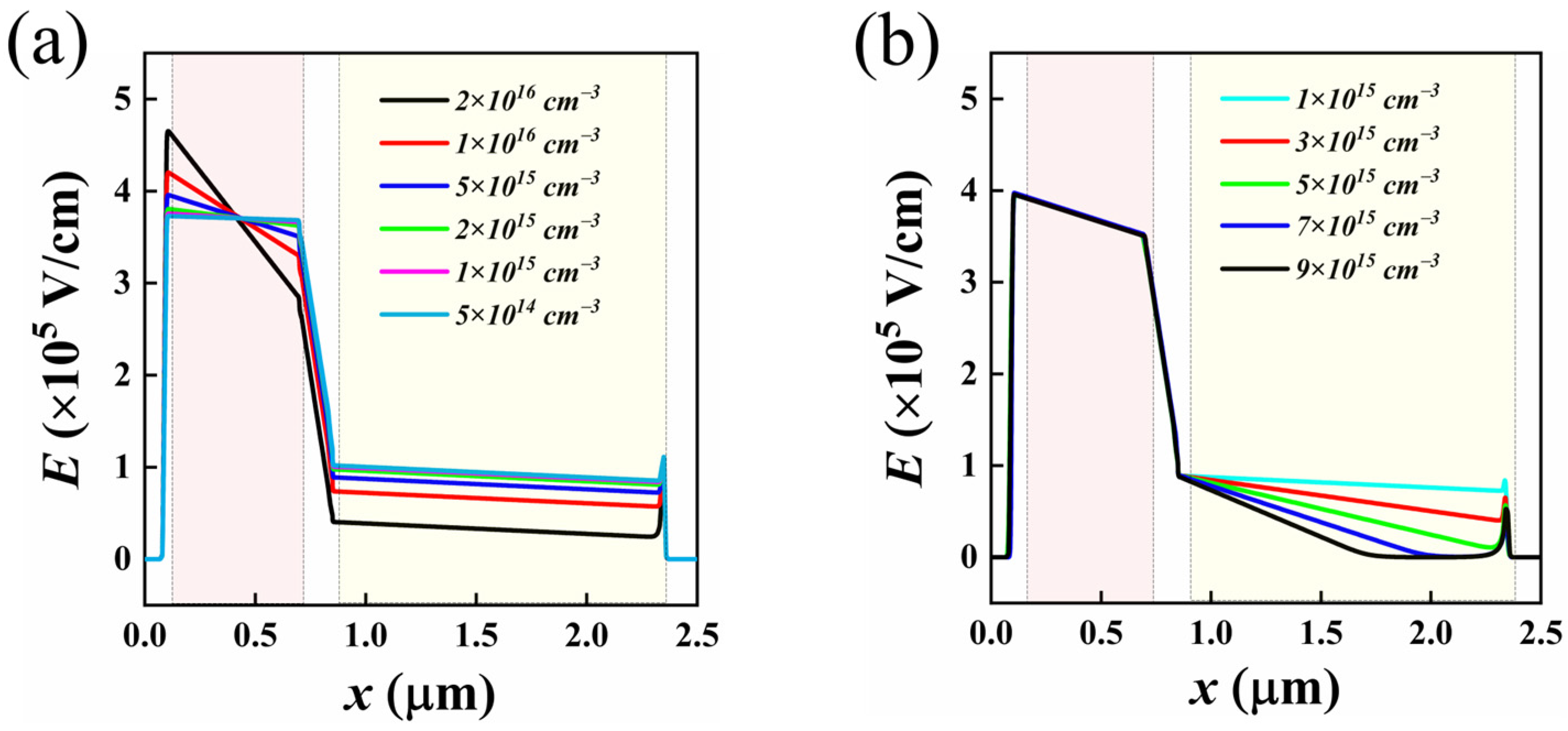
3.1. Parameter Design of Epitaxial Layer
3.2. Analysis of the Photoelectric Characteristics of Si/Ge-APD
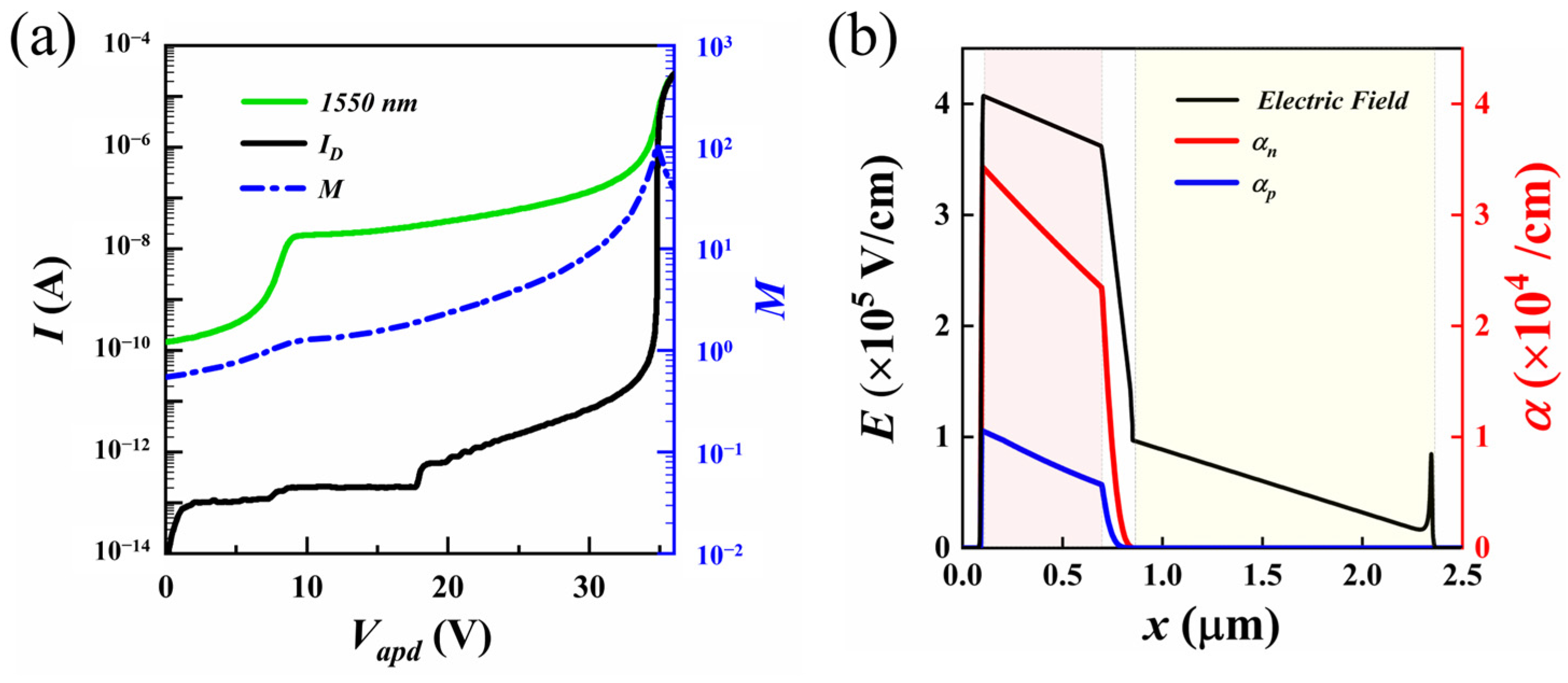
3.2.1. I–V Characteristics and Avalanche Multiplication Characteristics
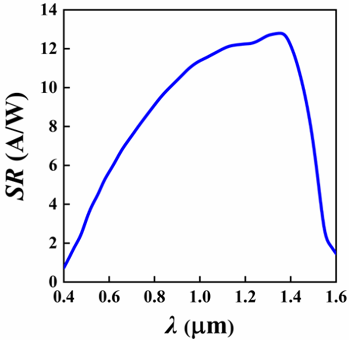
3.2.2. Spectral Responsivity Characteristics
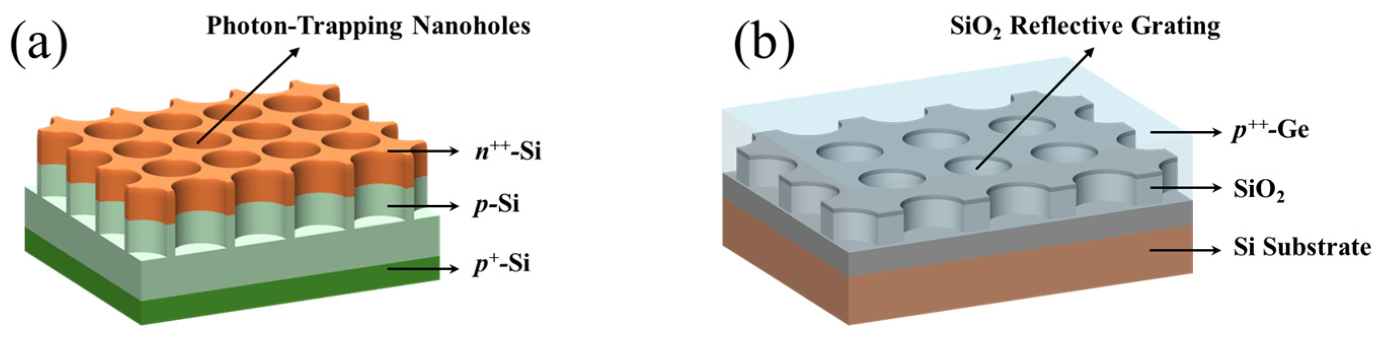
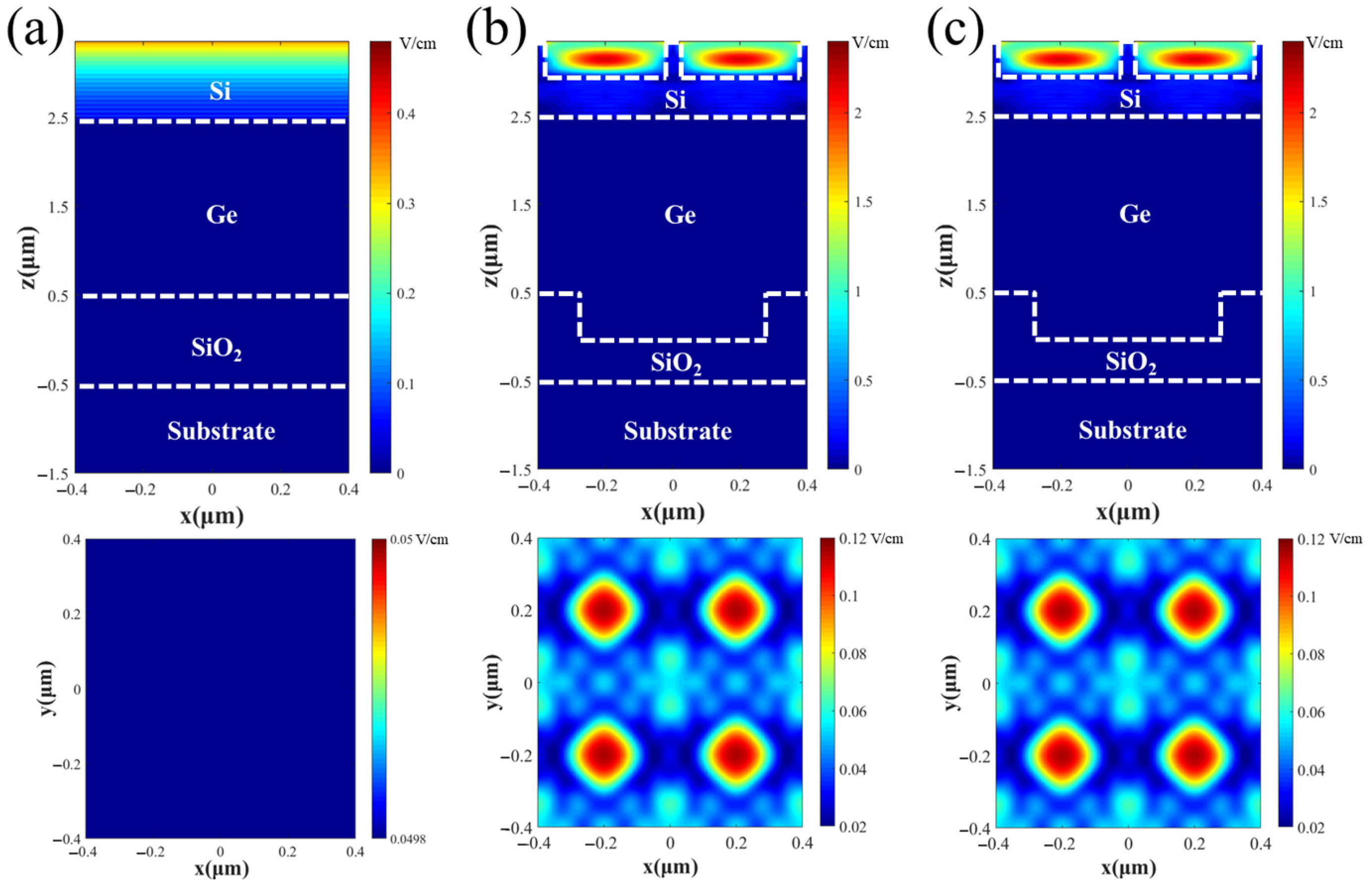
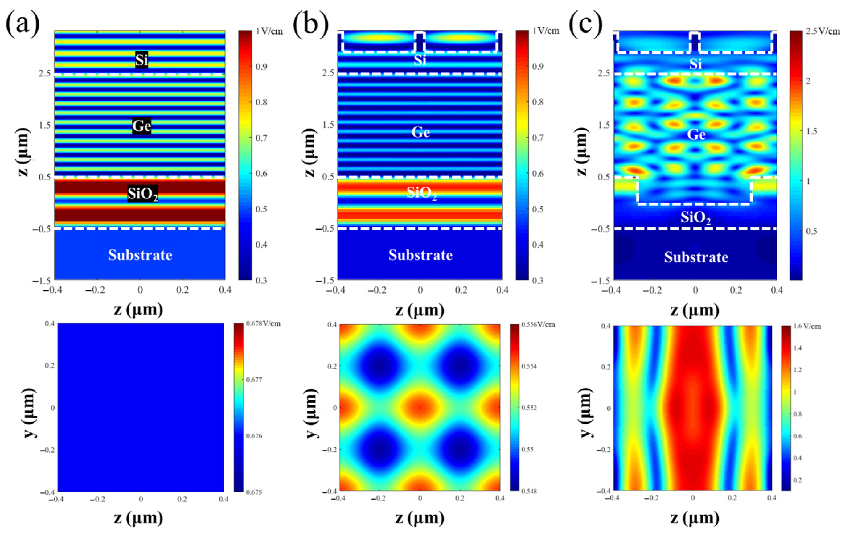
4. Design and Analysis of APD Light-Absorption-Enhancement Nanostructure
5. Conclusions
Supplementary Materials
Author Contributions
Funding
Institutional Review Board Statement
Informed Consent Statement
Data Availability Statement
Conflicts of Interest
References
- Hakkel, K.D.; Petruzzella, M.; Ou, F.; van Klinken, A.; Pagliano, F.; Liu, T.; van Veldhoven, R.P.J.; Fiore, A. Integrated near-infrared spectral sensing. Nat. Commun. 2022, 13, 103. [Google Scholar] [CrossRef] [PubMed]
- Ngo, N.H.; Nguyen, A.Q.; Bufler, F.M.; Kamakura, Y.; Mutoh, H.; Shimura, T.; Hosoi, T.; Watanabe, H.; Matagne, P.; Shimonomura, K.; et al. Toward the super temporal resolution image sensor with a germanium photodiode for visible light. Sensors 2020, 20, 6895. [Google Scholar] [CrossRef] [PubMed]
- Minotto, A.; Haigh, P.A.; Łukasiewicz, Ł.G.; Lunedei, E.; Gryko, D.T.; Darwazeh, I.; Cacialli, F. Visible light communication with efficient far-red/near-infrared polymer light-emitting diodes. Light Sci. Appl. 2020, 9, 70. [Google Scholar] [CrossRef]
- Pan, T.; Lu, D.; Xin, H.; Li, B. Biophotonic probes for bio-detection and imaging. Light Sci. Appl. 2021, 10, 124. [Google Scholar] [CrossRef]
- Zhuge, Q.; Chen, X.; Plant, D.V.; Shieh, W. Feature issue introduction: Ultra-wideband optical communications. Opt. Express 2022, 30, 13591–13593. [Google Scholar] [CrossRef]
- Assefa, S.; Xia, F.; Bedell, S.W.; Zhang, Y.; Topuria, T.; Rice, P.M.; Vlasov, Y.A. CMOS-integrated high-speed MSM germanium waveguide photodetector. Opt. Express 2010, 18, 4986–4999. [Google Scholar] [CrossRef] [PubMed]
- Chaisakul, P.; Marris-Morini, D.; Frigerio, J.; Chrastina, D.; Rouifed, M.S.; Cecchi, S.; Crozat, P.; Isella, G.; Vivien, L. Integrated germanium optical interconnects on silicon substrates. Nat. Photonics 2014, 8, 482–488. [Google Scholar] [CrossRef]
- Yin, T.; Cohen, R.; Morse, M.M.; Sarid, G.; Chetrit, Y.; Rubin, D.; Paniccia, M.J. 31 GHz Ge nip waveguide photodetectors on Silicon-on-Insulator substrate. Opt. Express 2007, 15, 13965–13971. [Google Scholar] [CrossRef] [PubMed]
- Kang, Y.; Liu, H.D.; Morse, M.; Paniccia, M.J.; Zadka, M.; Litski, S.; Sarid, G.; Pauchard, A.; Kuo, Y.-H.; Chen, H.-W.; et al. Monolithic germanium/silicon avalanche photodiodes with 340 GHz gain–bandwidth product. Nat. Photonics 2009, 3, 59–63. [Google Scholar] [CrossRef]
- Huang, Z.; Li, C.; Liang, D.; Yu, K.; Santori, C.; Fiorentino, M.; Sorin, W.; Palermo, S.; Beausoleil, R.G. 25 Gbps low-voltage waveguide Si–Ge avalanche photodiode. Optica 2016, 3, 793–798. [Google Scholar] [CrossRef]
- Yi, L.; Liu, D.; Li, D.; Zhang, P.; Tang, B.; Li, B.; Wang, W.; Yang, Y.; Li, Z. Waveguide-integrated Ge/Si avalanche photodiode with wertical multiplication region for 1310 nm detection. Photonics 2023, 10, 750. [Google Scholar] [CrossRef]
- Vines, P.; Kuzmenko, K.; Kirdoda, J.; Dumas, D.C.; Mirza, M.M.; Millar, R.W.; Paul, D.J.; Buller, G.S. High performance planar germanium-on-silicon single-photon avalanche diode detectors. Nat. Commun. 2019, 10, 1086. [Google Scholar] [CrossRef] [PubMed]
- Zeng, X.; Huang, Z.; Wang, B.; Liang, D.; Fiorentino, M.; Beausoleil, R.G. Silicon–germanium avalanche photodiodes with direct control of electric field in charge multiplication region. Optica 2019, 6, 772–777. [Google Scholar] [CrossRef]
- Liu, D.; Zhang, P.; Tang, B.; Wang, W.; Li, Z. High-performance waveguide-integrated Ge/Si avalanche photodetector with lateral multiplication region. Micromachines 2022, 13, 649. [Google Scholar] [CrossRef] [PubMed]
- Pang, Y.; Liu, Z.; Zhu, Y.; Liu, X.; Zhang, D.; Niu, C.; Li, M.; Zheng, J.; Zuo, Y.; Cheng, B. High-performance waveguide-coupled lateral Ge/Si avalanche photodetector. Opt. Lett. 2022, 47, 4463–4466. [Google Scholar] [CrossRef] [PubMed]
- Xiang, Y.; Cao, H.; Liu, C.; Dai, D. High-performance waveguide Ge/Si avalanche photodiode with a lateral separate-absorption-charge-multiplication structure. Opt. Express 2022, 30, 11288–11297. [Google Scholar] [CrossRef]
- Shi, Y.; Li, X.; Chen, G.; Zou, M.; Cai, H.; Yu, Y.; Zhang, X. Avalanche photodiode with ultrahigh gain–bandwidth product of 1033 GHz. Nat. Photonics 2024, 18, 610–616. [Google Scholar] [CrossRef]
- Wang, J.; Wang, X.; Li, Y.; Yang, Y.; Song, Q.; Xu, K. High-responsivity on-chip waveguide coupled germanium photodetector for 2 μm waveband. Photonics Res. 2023, 12, 115–122. [Google Scholar] [CrossRef]
- Cao, H.; Xiang, Y.; Sun, W.; Xie, J.; Guo, J.; Yu, Z.; Liu, L.; Shi, Y.; Dai, D. High-power Ge/Si waveguide photodetector. ACS Photonics 2024, 11, 1761–1770. [Google Scholar] [CrossRef]
- Simola, E.T.; De Iacovo, A.; Frigerio, J.; Ballabio, A.; Fabbri, A.; Isella, G.; Colace, L. Voltage-tunable dual-band Ge/Si photodetector operating in VIS and NIR spectral range. Opt. Express 2019, 27, 8529–8539. [Google Scholar] [CrossRef] [PubMed]
- De Iacovo, A.; Ballabio, A.; Frigerio, J.; Colace, L.; Isella, G. Design and simulation of Ge-on-Si photodetectors with electrically tunable spectral response. J. Lightwave Technol. 2019, 37, 3517–3525. [Google Scholar] [CrossRef]
- De Iacovo, A.; Mitri, F.; Ballabio, A.; Frigerio, J.; Isella, G.; Ria, A.; Cicalini, M.; Bruschi, P.; Colace, L. Dual-band Ge-on-Si photodetector array with custom, integrated readout electronics. IEEE Sens. J. 2022, 22, 3172–3180. [Google Scholar] [CrossRef]
- Michel, J.; Liu, J.; Kimerling, L.C. High-performance Ge-on-Si photodetectors. Nat. Photonics 2010, 4, 527–534. [Google Scholar] [CrossRef]
- Li, C.; Li, X.; Cai, Y.; Wang, W.; Yu, M. Design and optimization of high-responsivity high-speed Ge/Si avalanche photodiode in the C+L Band. Micromachines 2023, 14, 108. [Google Scholar] [CrossRef] [PubMed]
- Kim, G.; Kim, S.; Kim, S.A.; Oh, J.H.; Jang, K.S. NDR-effect vertical-illumination-type Ge-on-Si avalanche photodetector. Opt. Lett. 2018, 43, 5583–5586. [Google Scholar] [CrossRef]
- Deeb, H.; Khomyakova, K.; Kokhanenko, A.; Douhan, R.; Lozovoy, K. Dependence of Ge/Si avalanche photodiode performance on the thickness and doping concentration of the multiplication and absorption layers. Inorganics 2023, 11, 303. [Google Scholar] [CrossRef]
- Zhang, H.; Tian, Y.; Li, Q.; Ding, W.; Yu, X.; Lin, Z.; Feng, X.; Zhao, Y. Photon-trapping microstructure for InGaAs/Si avalanche photodiodes operating at 1.31 μm. Sensors 2022, 22, 7724. [Google Scholar] [CrossRef] [PubMed]
- Yakimov, A.I.; Kirienko, V.V.; Bloshkin, A.A.; Utkin, D.E.; Dvurechenskii, A.V. Near-infrared photoresponse in Ge/Si quantum dots enhanced by photon-trapping hole arrays. Nanomaterials 2021, 11, 2302. [Google Scholar] [CrossRef] [PubMed]
- Sha, Y.; Xie, H.; Xiang, Y.; Ji, R.; Zhu, F.; Shen, X.; Na, W.; Jin, D.; Zhang, W. High-efficiency SiGe/Si heterojunction phototransistor with photon-trapping nanoholes operating at 600–1000-nm wavelength. IEEE Trans. Electron Devices 2022, 69, 2514–2520. [Google Scholar] [CrossRef]
- Schlipf, J.; Berkmann, F.; Yamamoto, Y.; Reichenbach, M.; Veleski, M.; Kawaguchi, Y.; Mörz, F.; Tomm, J.W.; Weißhaupt, D.; Fischer, I.A. Robust Si/Ge heterostructure metasurfaces as building blocks for wavelength-selective photodetectors. Appl. Phys. Lett. 2023, 122, 121701. [Google Scholar] [CrossRef]
- Wu, S.; Zhou, H.; He, L.; Wang, Z.; Chen, Q.; Zhang, L.; Tan, C.S. Ge-on-Si avalanche photodiodes with photon trapping nanostructures for sensing and optical quantum applications. IEEE Sens. J. 2023, 24, 17604–17612. [Google Scholar] [CrossRef]
- Cansizoglu, H.; Bartolo-Perez, C.; Gao, Y.; Ponizovskaya Devine, E.; Ghandiparsi, S.; Polat, K.G.; Mamtaz, H.H.; Yamada, T.; Elrefaie, A.F.; Wang, S.-Y.; et al. Surface-illuminated photon-trapping high-speed Ge-on-Si photodiodes with improved efficiency up to 1700 nm. Photonics Res. 2018, 6, 734–742. [Google Scholar] [CrossRef]
- Ponizovskaya-Devine, E.; Mayet, A.S.; Rawat, A.; Ahamed, A.; Wang, S.Y.; Elrefaie, A.F.; Yamada, T.; Islam, M.S. Single microhole per pixel for thin Ge-on-Si complementary metal-oxide semiconductor image sensor with enhanced sensitivity up to 1700 nm. J. Nanophotonics 2023, 17, 016012. [Google Scholar] [CrossRef]
- Zeng, L.; Bermel, P.; Yi, Y.; Alamariu, B.A.; Broderick, K.A.; Liu, J.; Hong, C.; Duan, X.; Joannopoulos, J.; Kimerling, L.C. Demonstration of enhanced absorption in thin film Si solar cells with textured photonic crystal back reflector. Appl. Phys. Lett. 2008, 93, 221105. [Google Scholar] [CrossRef]
- Chuah, L.S. Enhanced light management of thin film solar cells with ZnO back reflector. AIP Conf. Proc. 2024, 2895, 050001. [Google Scholar]
- Heidarzadeh, H.; Tavousi, A. Performance enhancement methods of an ultra-thin silicon solar cell using different shapes of back grating and angle of incidence light. Mater. Sci. Eng. B 2019, 240, 1–6. [Google Scholar] [CrossRef]
- Sheng, X.; Broderick, L.Z.; Kimerling, L.C. Photonic crystal structures for light trapping in thin-film Si solar cells: Modeling, process and optimizations. Opt. Commun. 2014, 314, 41–47. [Google Scholar] [CrossRef]
- Sze, S.M.; Li, Y.; Ng, K.K. Physics of Semiconductor Devices, 3rd ed.; Xi’an Jiaotong University Press: Xi’an, China, 2008. [Google Scholar]
- Miller, S.L. Avalanche breakdown in germanium. Phys. Rev. 1955, 99, 1234. [Google Scholar] [CrossRef]
- Duan, N.; Liow, T.Y.; Lim, A.E.J.; Ding, L.; Lo, G. 310 GHz gain-bandwidth product Ge/Si avalanche photodetector for 1550 nm light detection. Opt. Express 2012, 20, 11031–11036. [Google Scholar] [CrossRef] [PubMed]
- Huang, M.; Li, S.; Cai, P.; Hou, G.; Su, T.I.; Chen, W.; Hong, C.-Y.; Pan, D. Germanium on silicon avalanche photodiode. IEEE J. Sel. Top. Quantum Electron. 2017, 24, 1–11. [Google Scholar] [CrossRef]
- Song, J.; Yuan, S.; Cui, C.; Li, Y.; Zeng, C.; Xia, J. Photonic crystal enabled manipulation of optical and electric field in germanium avalanche photodetectors. Nanotechnology 2021, 32, 145201. [Google Scholar] [CrossRef] [PubMed]
- Li, C.; Xue, C.; Liu, Z.; Cong, H.; Cheng, B.; Hu, Z.; Guo, X.; Liu, W. High-responsivity vertical-illumination Si/Ge uni-traveling-carrier photodiodes based on silicon-on-insulator substrate. Sci. Rep. 2016, 6, 27743. [Google Scholar] [CrossRef] [PubMed]
- Zhang, J.; Zhu, S.; Sun, F. Dual-epitaxy Si/Ge broadband photodetector for application in cryogenic radiometer. Opt. Express 2021, 29, 37489–37502. [Google Scholar] [CrossRef] [PubMed]
- Palik, E.D. Handbook of Optical Constants of Solids; Academic Press: Cambridge, MA, USA, 1985. [Google Scholar]
- Woods, M.H.; Johnson, W.C.; Lampert, M.A. Use of a Schottky barrier to measure impact ionization coefficients in semiconductors. Solid-State Electron. 1973, 16, 381–394. [Google Scholar] [CrossRef]
- Saleh, B.E.; Teich, M.C. Fundamentals of Photonics; John Wiley & Sons: Hoboken, NJ, USA, 1991. [Google Scholar]


| Reference | Device Type | Device Structure | Responsivity (A/W) | Response Band (μm) | Peak Response(A/W) | Dark Current (μA) | VBR (V) | Multiplication Coefficient |
| [24] S | APD | p+(Ge)-i(Ge)-p(Si)-i(Si)-n+(Si) | 14.7 at 1.55 μm (@−19.2 V) | 1.3–1.7 | 14.7 (1.55 μm) | 7.85 (@−19.2 V) | −20.2 | 18.4 (@−19.2 V) |
| [25] | APD | p+(Ge)-i(Ge)-i(Si)-p(Si)-i(Si)-n+(Si) | 19.5 at 1.55 μm (@−26.8 V) | / | / | 78 (@−26.8 V) | −26.8 | 55.7 (@−26.8 V) |
| [26] S | APD | p+(Ge)-p(Ge)-p(Si)-n(Si)-n+(Si) | 60 * at 1.31 μm (@−26 V) | 0.4–1.6 | 54 * (0.9 μm,@−26 V) | / | −26 | 60 * (@−26 V) |
| [40] | APD | p+(Si)-i(Ge)-p(Si)-n(Si) | 12 at 1.55 μm (@−29 V) | / | / | 5 * (@−27 V) | −29.4 | 39 * (@−29 V) |
| [41] | APD | p+(Si)-i(Ge)-p(Si)-i(Si)-n(Si) | 8.7 at 1.55 μm (@−21 V) | / | / | 3 (@−27 V) | −28.5 | 12 (@−27 V) |
| [31] | APD with photon trap | p+(Ge)-i(Ge)-p(Si)-i(Si)-n+(Si) | 4.5 at 1.55 μm (@−16 V) | / | / | 1 * (@−4 V) | −16 | 20 * (@−16 V) |
| [42] | APD with photon trap | n+(Ge)-i(Ge)-p+(Ge)-p+(Si) | 0.6 at 1.55 μm (@−0.1 V) | / | / | 100 * (@−8.6 V) | −8.8 | 14 * (@−8.8 V) |
| [43] | Photodiode | p(Ge)-i(Si)-n+(Si) | 0.18 at 1.55 μm (@−1 V) | / | / | 0.058 (@−1 V) | ||
| [44] | Photodiode | p+(Si)-i(Si)-i(Ge)-n+(Si) | 0.27 * at 1.55 μm (@−0 V) | 0.4–1.6 | 0.62 * (1 μm, @0 V) | 130 (@−2 V) | ||
| [29] S | Photodiode with photon trap | n+(Si)-p+(SiGe)-n−(Si)-n+(Si) | 27.02 at 0.85 μm (@−3 V) | 0.6–1.0 | / | 2.6 × 10⁻⁷ (@−2 V) | ||
| [32] | Photodiode with photon trap | p+(Ge)-i(Ge)-n+(Si) | 0.91 at 1.55 μm (@−1 V) | 1.2–1.7 | 0.98 * (1.48 μm, @0 V) | 1.0 * (@−1 V) | ||
| This Work | APD with photon trap and reflection grating | n++(Si)-p(Si)-p+(Si)-π(Ge)-p++(Ge) | 2.9 at 0.45 μm; 10.9 at 0.85 μm; 17.6 at 1.55 μm (@−33.1 V) | 0.4–1.6 | 25 (1.46 μm, @−33.1 V) | 2.1 × 10⁻⁵ (@−33.1 V) | −34.83 | 104 (@−34.83 V) |
Disclaimer/Publisher’s Note: The statements, opinions and data contained in all publications are solely those of the individual author(s) and contributor(s) and not of MDPI and/or the editor(s). MDPI and/or the editor(s) disclaim responsibility for any injury to people or property resulting from any ideas, methods, instructions or products referred to in the content. |
© 2025 by the authors. Licensee MDPI, Basel, Switzerland. This article is an open access article distributed under the terms and conditions of the Creative Commons Attribution (CC BY) license (https://creativecommons.org/licenses/by/4.0/).
Share and Cite
Guo, G.; Chen, W.; Zheng, K.; Lv, J.; Chen, Y.; Zhao, B.; Zhao, Y.; Qin, Y.; Wang, X.; Gao, D.; et al. Research on High-Responsivity Si/Ge-APD in Visible–Near-Infrared Wide Spectrum with Light-Absorption-Enhanced Nanostructure. Sensors 2025, 25, 1167. https://doi.org/10.3390/s25041167
Guo G, Chen W, Zheng K, Lv J, Chen Y, Zhao B, Zhao Y, Qin Y, Wang X, Gao D, et al. Research on High-Responsivity Si/Ge-APD in Visible–Near-Infrared Wide Spectrum with Light-Absorption-Enhanced Nanostructure. Sensors. 2025; 25(4):1167. https://doi.org/10.3390/s25041167
Chicago/Turabian StyleGuo, Guangtong, Weishuai Chen, Kaifeng Zheng, Jinguang Lv, Yupeng Chen, Baixuan Zhao, Yingze Zhao, Yuxin Qin, Xuefei Wang, Dan Gao, and et al. 2025. "Research on High-Responsivity Si/Ge-APD in Visible–Near-Infrared Wide Spectrum with Light-Absorption-Enhanced Nanostructure" Sensors 25, no. 4: 1167. https://doi.org/10.3390/s25041167
APA StyleGuo, G., Chen, W., Zheng, K., Lv, J., Chen, Y., Zhao, B., Zhao, Y., Qin, Y., Wang, X., Gao, D., Liang, J., & Wang, W. (2025). Research on High-Responsivity Si/Ge-APD in Visible–Near-Infrared Wide Spectrum with Light-Absorption-Enhanced Nanostructure. Sensors, 25(4), 1167. https://doi.org/10.3390/s25041167