
An Anisotropic Equivalent Thermal Model for Shield Differential Through-Silicon Vias


Abstract
:1. Introduction
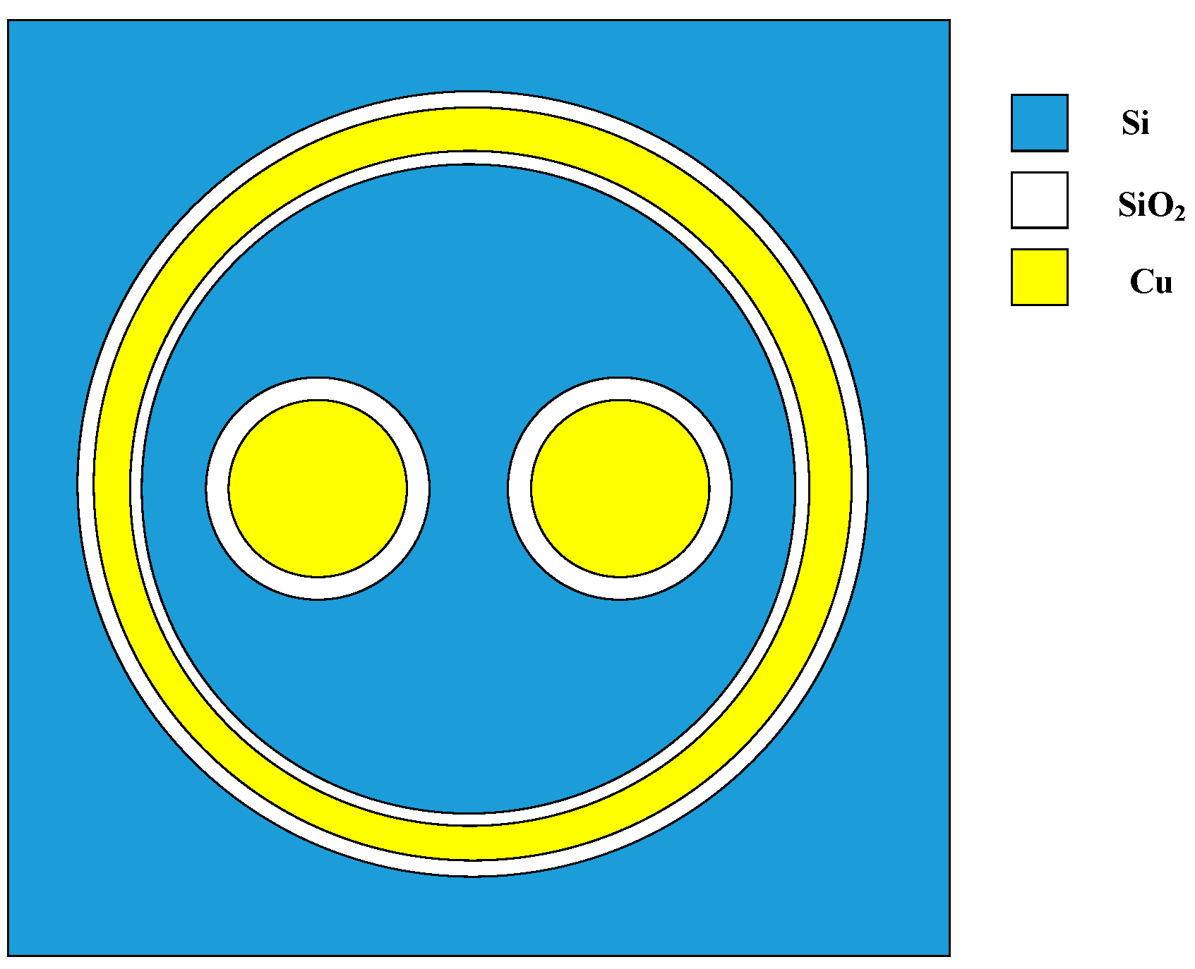
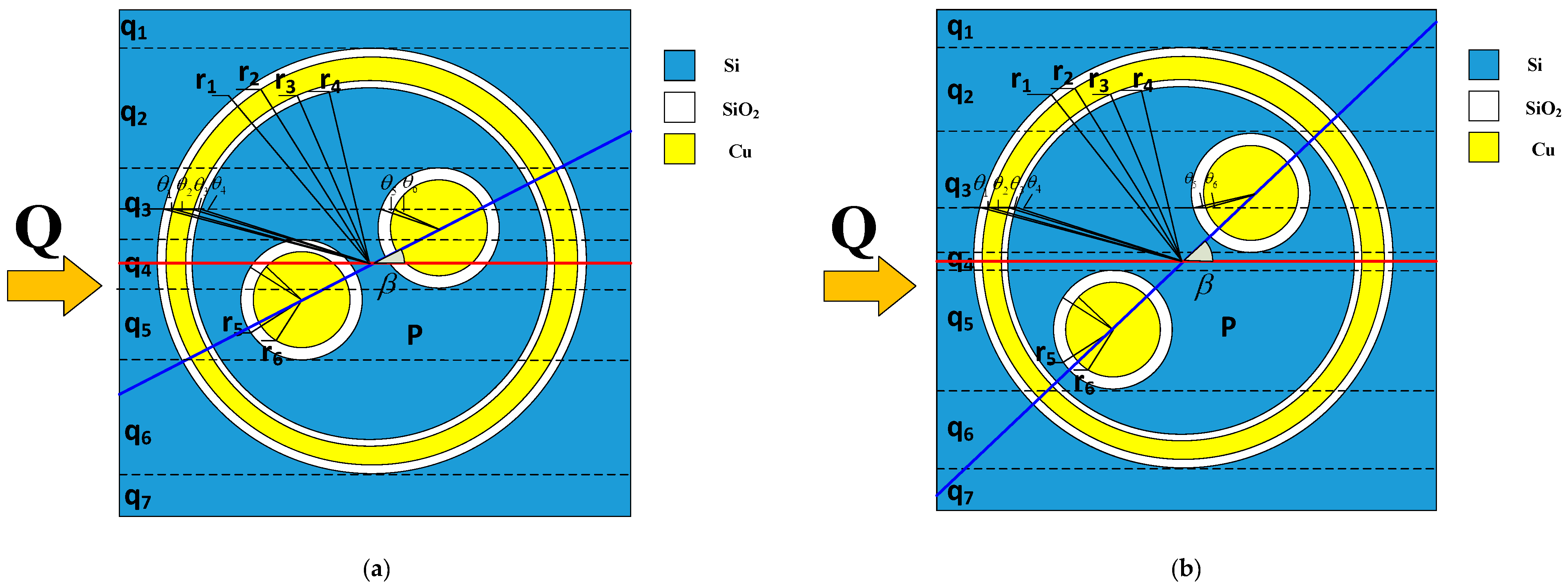
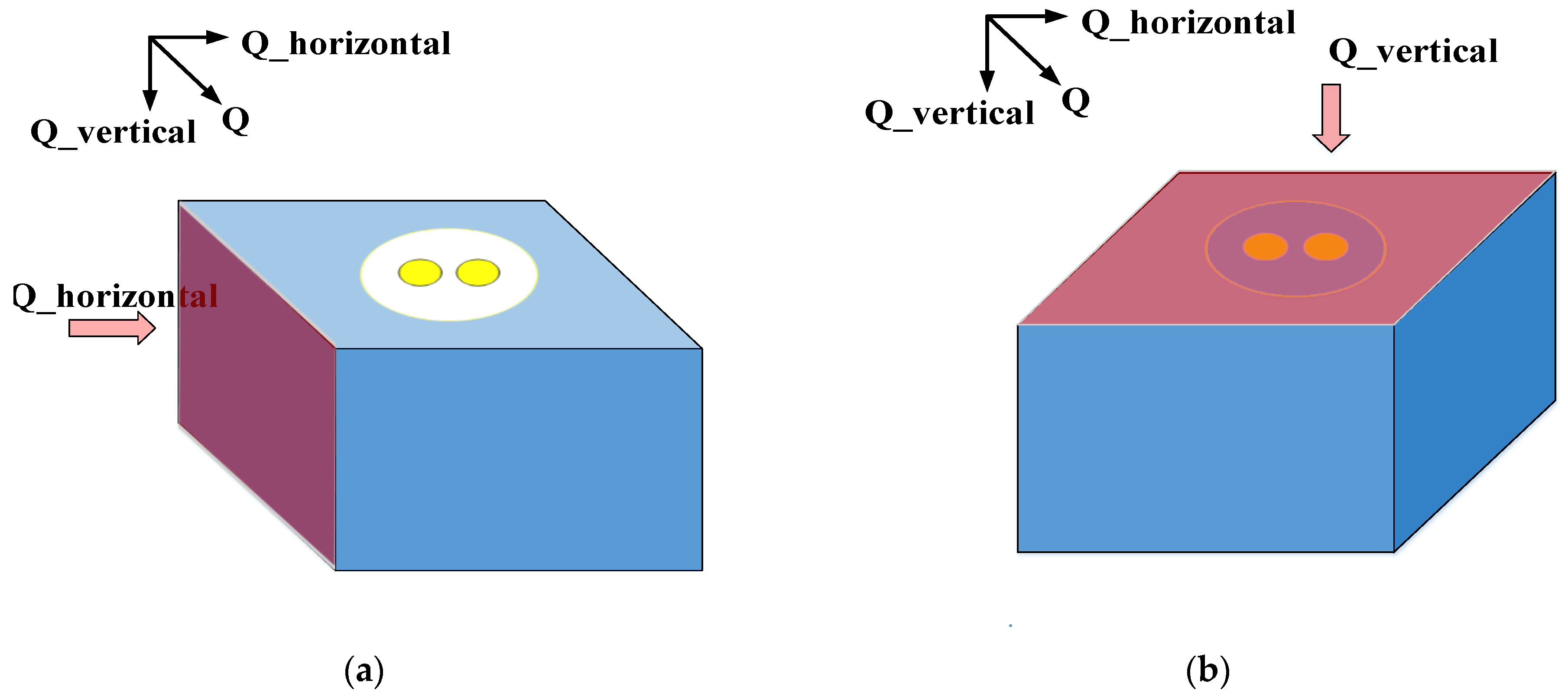
2. Expressions for Equivalent Thermal Conductivities of SDTSV
3. Model Validation and Discussion
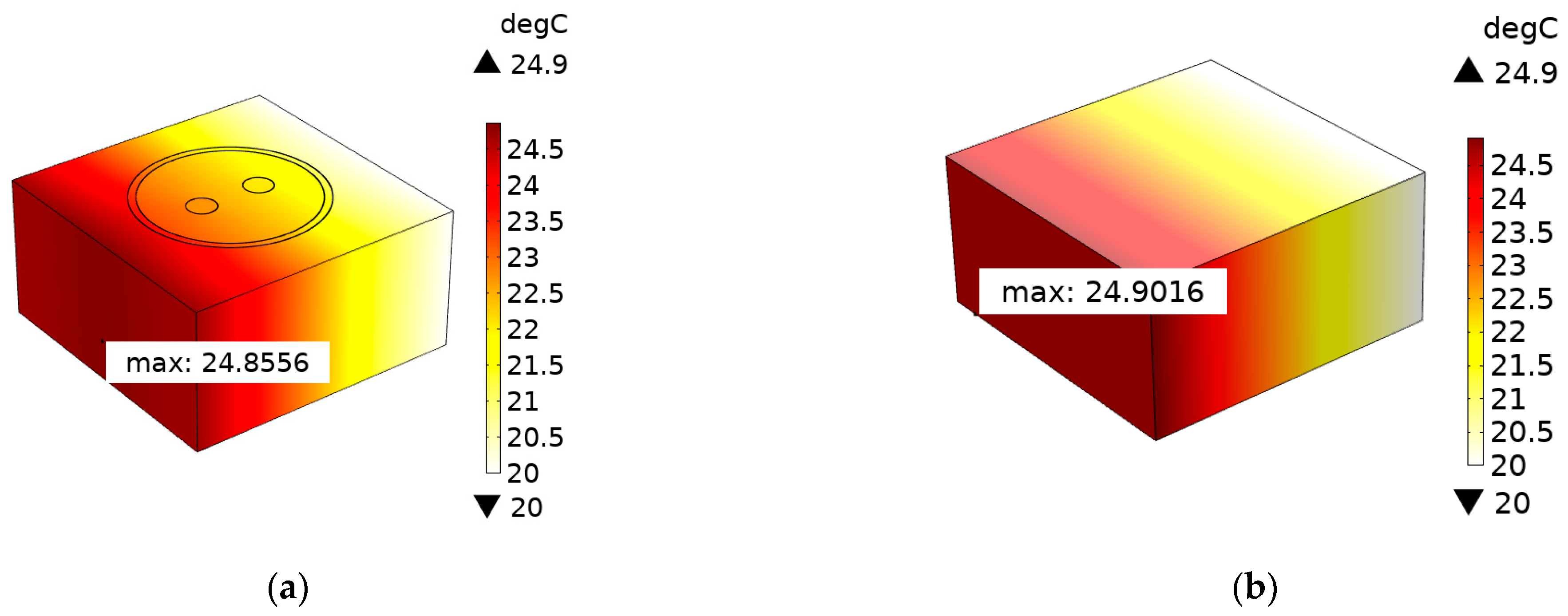
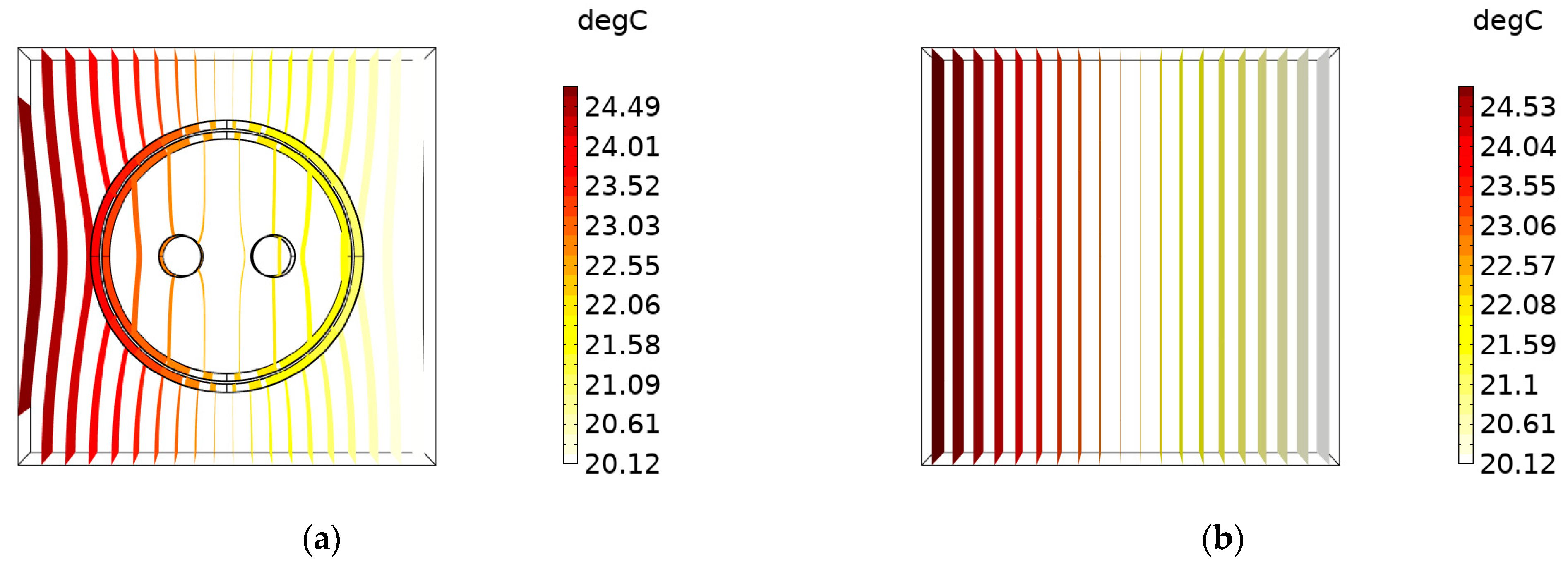
3.1. Numerical Validation
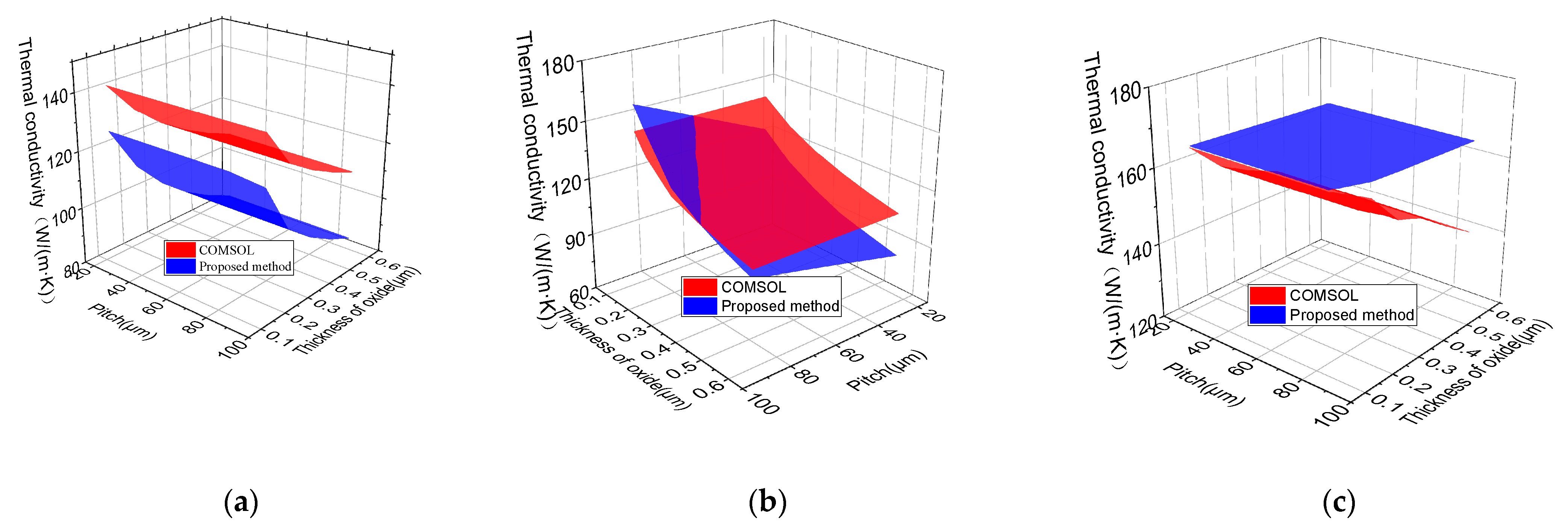
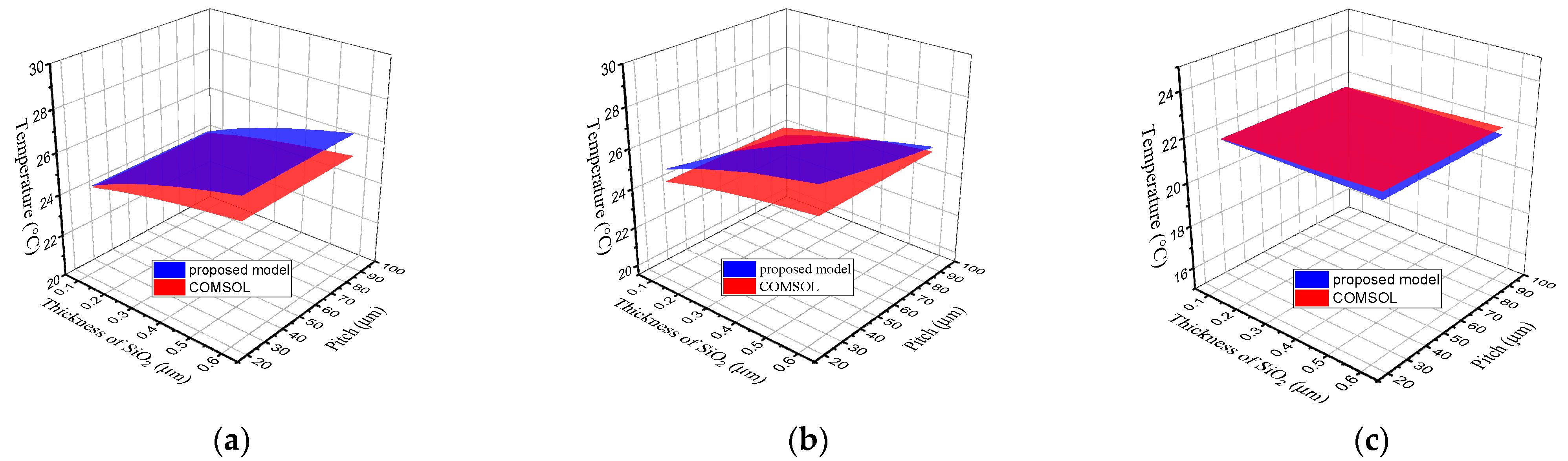
3.2. Effects of Different Parameters on the Temperature Distribution of SDTSV
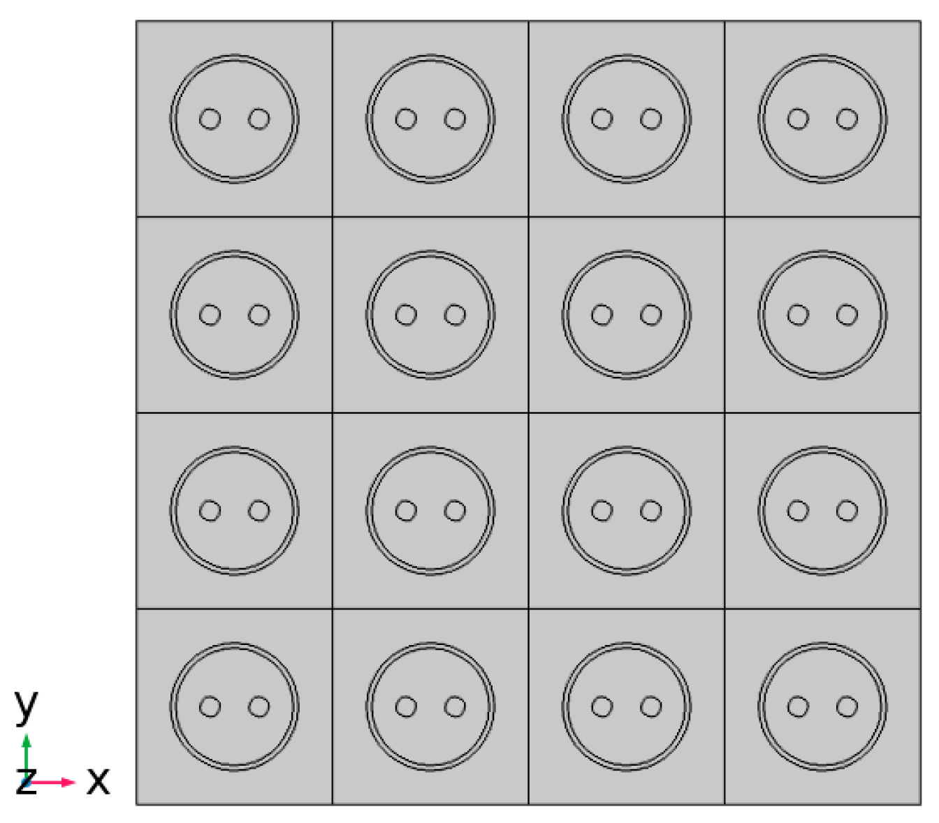
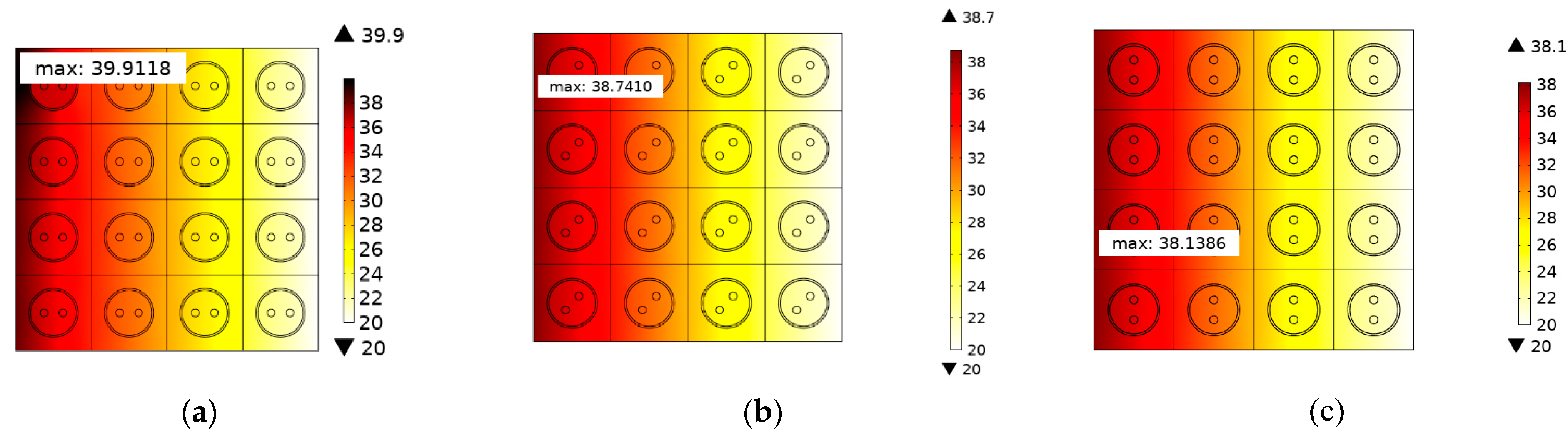
3.3. Thermal Distribution of SDTSV Array
3.4. Discussion and Analysis
4. Conclusions
- (1)
- An accurate equivalent thermal model is established for SDTSV, which can describe the thermal distribution of SDTSV along an arbitrary angle. The mathematical expressions of ETC in horizontal and vertical directions are deduced;
- (2)
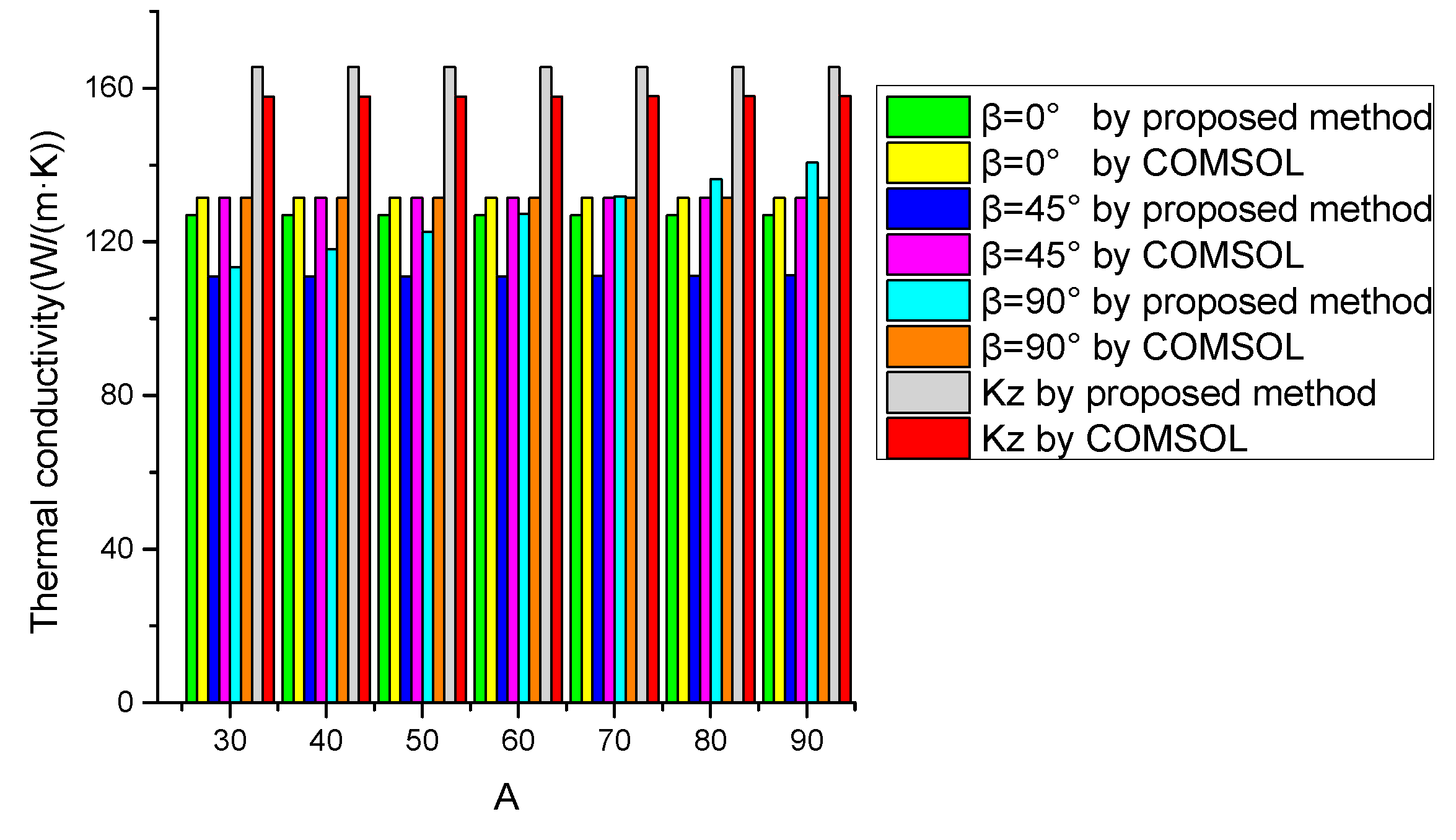
- The accuracy of the proposed model is verified by COMSOL, and the average errors of temperature at , , and vertical directions are 1.37%, 3.42%, 1.76%, and 0.40%, respectively. In addition, the calculation time of the proposed model is reduced from approximately 300 s to 1.92 s;
- (3)
- The effects of different parameters on the thermal distribution of SDTSV are investigated based on the proposed model. As the pitch increases, the maximum temperature of SDTSV increases very slowly when β = 0 , and decreases very slowly when β = 90; however, the ETC decreases as the thickness of SiO2 increases.
Author Contributions
Funding
Conflicts of Interest
References
- Liu, H.; Fang, R.; Miao, M.; Jin, Y. Accurate Modeling of the Capacitance of Through Silicon Via Considering Minority Carrier Effects. IEEE Trans. Compon. Packag. Manuf. Technol. 2020, 99, 749–762. [Google Scholar] [CrossRef]
- Pan, Y.; Li, F.; He, H.; Li, J.; Zhu, W. Effects of dimension parameters and defect on TSV thermal behavior for 3D IC packaging. Microelectron. Reliab. 2017, 70, 97–102. [Google Scholar] [CrossRef]
- Wang, M.; Ma, S.; Jin, Y.; Wang, W.; Chen, J.; Hu, L.; He, S. A RF Redundant TSV Interconnection for High Resistance Si Interposer. Micromachines 2021, 12, 169. [Google Scholar] [CrossRef]
- Shan, G.; Lu, Q.; Liu, S.; Yang, Y. Through-Silicon Capacitor Interconnection for High-Frequency 3-D Microsystem. IEEE Trans. Compon. Packag. Manuf. Technol. 2019, 9, 1310–1318. [Google Scholar] [CrossRef]
- Jin, J.; Zhao, W.S.; Wang, D.W.; Chen, H.S.; Li, E.P.; Yin, W.Y. Investigation of Carbon Nanotube-Based Through-Silicon Vias for PDN Applications. IEEE Trans. Electromagn. Compat. 2018, 60, 638–646. [Google Scholar] [CrossRef]
- Li, H.; Liu, J.; Xu, T.; Xia, J.; Tan, X.; Tao, Z. Fabrication and Optimization of High Aspect Ratio Through-Silicon-Vias Electroplating for 3D Inductor. Micromachines 2018, 9, 528. [Google Scholar] [CrossRef] [Green Version]
- Chiang, T.Y. Thermal analysis of heterogeneous 3D ICs with various integration scenarios. In Proceedings of the International Electronics Devices Meeting, Washington, DC, USA, 2–5 December 2001; pp. 31.2.1–31.2.4. [Google Scholar]
- Yue, Q.; Lu, Z.; Dou, W. From 2D to 3D NoCs: A case study on worst-case communication performance. In Proceedings of the International Conference Computer-Aided Design, San Jose, CA, USA, 2–5 November 2009; pp. 555–562. [Google Scholar]
- Wang, S.; Yin, Y.; Hu, C.; Rezai, P. 3D Integrated Circuit Cooling with Microfluidics. Micromachines 2018, 9, 287. [Google Scholar] [CrossRef] [PubMed] [Green Version]
- Chan, J.M.; Lee, K.C.; Tan, C.S. Effects of Copper Migration on the Reliability of Through-Silicon Via (TSV). IEEE Trans. Device Mater. Reliab. 2018, 18, 520–528. [Google Scholar] [CrossRef]
- Lu, Q.; Zhu, Z.; Yang, Y.; Ding, R. Electrical Modeling and Characterization of Shield Differential Through-Silicon Vias. IEEE Trans. Electron Devices 2015, 62, 1544–1552. [Google Scholar]
- Salvi, S.S.; Jain, A. A Review of Recent Research on Heat Transfer in Three-Dimensional Integrated Circuits (3D ICs). IEEE Trans. Compon. Packag. Manuf. Technol. 2021, 11, 802–821. [Google Scholar] [CrossRef]
- Ren, Z.; Alqahtani, A.; Bagherzadeh, N.; Lee, J. Thermal TSV Optimization and Hierarchical Floorplanning for 3D Integrated Circuits. IEEE Trans. Compon. Packag. Manuf. Technol. 2020, 4, 599–610. [Google Scholar] [CrossRef]
- Lu, T.; Zhang, F.; Jin, J.M. Multiphysics Simulation of 3-D ICs With Integrated Microchannel Cooling. IEEE Trans. Compon. Packag. Manuf. Technol. 2016, 6, 1620–1629. [Google Scholar] [CrossRef]
- Alqahtani, A.; Ren, Z.; Lee, J.; Bagherzadeh, N. System-Level Analysis of 3D ICs with Thermal TSVs. ACM J. Emerg. Technol. Comput. Syst. 2018, 14, 37. [Google Scholar] [CrossRef]
- Ren, Z.; Yu, Z.; Kim, J.C.; Lee, J. TSV-integrated thermoelectric cooling by holey silicon for hot spot thermal management. Nanotechnology 2018, 30, 035201. [Google Scholar] [CrossRef]
- Pi, Y.; Wang, N.; Chen, J.; Miao, M.; Jin, Y.; Wang, W. Anisotropic equivalent thermal conductivity model for efficient and accurate full-chip-scale numerical simulation of 3D stacked IC. Int. J. Heat Mass Transf. 2018, 120, 361–378. [Google Scholar] [CrossRef]
- Sridhar, A.; Vincenzi, A.; Ruggiero, M.; Brunschwiler, T.; Atienza, D. 3D-ICE: Fast compact transient thermal modeling for 3D ICs with inter-tier liquid cooling. In Proceedings of the 2010 International Conference Computer-Aided Design (ICCAD), San Jose, CA, USA, 7–11 November 2010; pp. 463–470. [Google Scholar]
- Hu, X.; Ma, S.; Gong, D.; Wang, M.; Jin, Y.; Wang, W.; Chen, J.; He, S.; Hu, L.; Zhou, B. Thermal resistance analysis for a high power 3D integrated RF Module based on TSV interposer. In Proceedings of the 21st Electronics Packaging Technology Conference (EPTC 2019), Singapore, 4–6 December 2019. [Google Scholar]
- Xiao, C.; He, H.; Li, J.; Cao, S.; Zhu, W. An effective and efficient numerical method for thermal management in 3D stacked integrated circuits. Appl. Therm. Eng. 2017, 121, 200–209. [Google Scholar] [CrossRef]
- Chien, H.C.; Lau, J.H.; Chao, Y.L.; Tain, R.M.; Dai, M.J.; Wu, S.T.; Lo, W.O.; Kao, M.J. Thermal performance of 3D IC integration with Through-Silicon Via (TSV). In Proceedings of the International Symposium on Microelectronics 2011, Long Beach, CA, USA, 9–13 October 2011; Volume 1, pp. 25–32. [Google Scholar]
- Min, Q.; Li, E.P.; Jin, J.M.; Chen, W. Electrical–Thermal Cosimulation of Coaxial TSVs With Temperature-Dependent MOS Effect Using Equivalent Circuit Models. IEEE Trans. Electromagn. Compat. 2020, 62, 2247–2256. [Google Scholar] [CrossRef]
- Feng, Q.; Min, T.; Fu, G.; Mao, J. Fast transient thermal simulation of 2.5-D packages on through silicon via interposer. In Proceedings of the 2016 IEEE 20th Workshop on Signal and Power Integrity (SPI), Turin, Italy, 8–11 May 2016; pp. 1–4. [Google Scholar]
- Lau, J.H.; Yue, T.G. Thermal management of 3D IC integration with TSV (through silicon via). In Proceedings of the 2009 59th Electronic Components and Technology Conference, San Diego, CA, USA, 26–29 May 2009; pp. 635–640. [Google Scholar]
- Chien, H.C.; Lau, J.H.; Chao, Y.L.; Dai, M.J.; Brillhart, M. Thermal evaluation and analyses of 3D IC integration SiP with TSVs for network system applications. In Proceedings of the Electronic Components & Technology Conference, San Diego, CA, USA, 29 May–1 June 2012; pp. 1866–1873. [Google Scholar]
- Chen, Z.; Luo, X.; Liu, S. Thermal analysis of 3D packaging with a simplified thermal resistance network model and finite element simulation. In Proceedings of the 11th International Conference on Electronic Packaging Technology and High Density Packaging, Xi’an, China, 16–19 August 2010; pp. 737–741. [Google Scholar]
- Han, L.; Tong, Z. A thermal resistance network model based on three-dimensional structure. Measurement 2019, 133, 439–443. [Google Scholar] [CrossRef]
- Petrosyants, K.O.; Ryabov, N.I. Quasi-3D Thermal Simulation of Integrated Circuit Systems in Packages. Energies 2020, 13, 3054. [Google Scholar] [CrossRef]
- Wu, M.L.; Lan, J.S. Analytical and finite element methodology modeling of the thermal management of 3D IC with through silicon via. Solder. Surf. Mt. Technol. 2016, 28, 177–187. [Google Scholar] [CrossRef]
- Kai, F.; Zhao, W.S.; Wang, G.; Swaminathan, M. Modeling and Performance Analysis of Shielded Differential Annular Through-Silicon Via (SD-ATSV) for 3-D ICs. IEEE Access 2018, 6, 33238–33250. [Google Scholar]
- Zhao, W.S.; Hu, Q.H.; Fu, K.; Zhang, Y.Y.; Wang, G. Modeling of Carbon Nanotube-Based Differential Through-Silicon Vias in 3-D ICs. IEEE Trans. Nanotechnol. 2020, 19, 492–499. [Google Scholar] [CrossRef]
- Liao, C.; Zhu, Z.; Lu, Q.; Liu, X.; Yang, Y. Wideband Electromagnetic Model and Analysis of Shielded-Pair Through-Silicon Vias. IEEE Trans. Compon. Packag. Manuf. Technol. 2018, 8, 473–481. [Google Scholar] [CrossRef]
- Wei, H.; Wu, T.F.; Sekar, D.; Cronquist, B.; Pease, R.F.; Mitra, S. Cooling three-dimensional integrated circuits using power delivery networks. In Proceedings of the International Electron Devices Meeting. Technical Digest, San Francisco, CA, USA, 10–13 December 2012; pp. 14.2.1–14.2.4. [Google Scholar]
- Zhu, W.; Dong, G.; Yang, Y. Thermal-Aware Modeling and Analysis for a Power Distribution Network Including Through-Silicon-Vias in 3-D ICs. IEEE Trans. Comput.-Aided Des. Integr. Circuits Syst. 2019, 38, 1278–1290. [Google Scholar] [CrossRef]
- Liu, Z.; Swarup, S.; Tan, S.X.D.; Chen, H.B.; Wang, H. Compact Lateral Thermal Resistance Model of TSVs for Fast Finite-Difference Based Thermal Analysis of 3-D Stacked ICs. IEEE Trans. Comput.-Aided Des. Integr. Circuits Syst. 2014, 33, 1490–1502. [Google Scholar] [CrossRef]
- Wang, J.; Carson, J.K.; North, M.F.; Cleland, D.J. A new approach to modelling the effective thermal conductivity of heterogeneous materials. Int. J. Heat Mass Transf. 2006, 49, 3075–3083. [Google Scholar] [CrossRef]
- Jain, A.; Jones, R.E.; Chatterjee, R.; Pozder, S.; Huang, Z. Thermal modeling and design of 3D integrated circuits. In Proceedings of the 2008 11th Intersociety Conference on Thermal and Thermomechanical Phenomena in Electronic Systems, Orlando, FL, USA, 28–31 May 2008; pp. 1139–1145. [Google Scholar]


| Symbol | Definition |
|---|---|
| the height of TSV | |
| p | pitch between two inner signal TSVs |
| oxide thickness | |
| outer oxide radius of the shielding shell | |
| outer metal radius of the shielding shell (=r1 − tox) | |
| inner metal radius of the shielding shell | |
| inner oxide radius of the shielding shell (=r3 − tox) | |
| oxide radius of the TSV | |
| metal radius of the TSV (=r5 − tox) | |
| the thermal conductivity of Si | |
| the thermal conductivity of SiO2 | |
| the thermal conductivity of Cu | |
| a | the width of SDTSV cell |
| b | the length of SDTSV cell |
| Symbol | Definition | Value |
|---|---|---|
| the height of TSV | 100 μm | |
| oxide thickness | 0.2 μm | |
| outer oxide radius of the shielding shell | 10.2 μm | |
| outer metal radius of the shielding shell(=r1−tox) | 10 μm | |
| nner metal radius of the shielding shell | 60 μm | |
| inner oxide radius of the shielding shell(=r3−tox) | 59.8 μm | |
| oxide radius of the TSV | 65.2 μm | |
| metal radius of the TSV (=r5−tox) | 65 μm | |
| the thermal conductivity of Si | 150 | |
| the thermal conductivity of SiO2 | 1.38 | |
| the thermal conductivity of Cu | 400 | |
| a | the width of SDTSV cell | 200 μm |
| b | the length of SDTSV cell | 200 μm |
| Model | Max. Temperature (°C) | Av. Error | Av. Time (s) | ||||||||
|---|---|---|---|---|---|---|---|---|---|---|---|
| Pitch (μm) | 25 | 30 | 35 | 40 | 45 | 50 | 55 | 60 | - | - | |
| Proposed method | ° | 24.83 | 24.73 | 24.63 | 24.54 | 24.45 | 24.36 | 24.28 | 24.19 | 1.37% | 1.92 |
| 25.41 | 25.41 | 25.41 | 25.41 | 25.41 | 25.41 | 25.41 | 25.40 | 3.42% | 1.89 | ||
| 25.40 | 25.29 | 25.18 | 25.08 | 24.99 | 24.89 | 24.80 | 24.71 | 1.76% | 1.87 | ||
| Qz | 21.81 | 21.81 | 21.81 | 21.81 | 21.81 | 21.81 | 21.81 | 21.81 | 0.40% | 1.96 | |
| COMSOL | 24.56 | 24.56 | 24.56 | 24.56 | 24.56 | 24.57 | 24.57 | 24.57 | - | 297 | |
| 24.57 | 24.57 | 24.57 | 24.57 | 24.57 | 24.57 | 24.57 | 24.57 | - | 287 | ||
| 24.57 | 24.57 | 24.57 | 24.57 | 24.57 | 24.57 | 24.57 | 24.57 | - | 293 | ||
| Qz | 21.90 | 21.90 | 21.90 | 21.90 | 21.90 | 21.90 | 21.90 | 21.90 | - | 306 | |
Publisher’s Note: MDPI stays neutral with regard to jurisdictional claims in published maps and institutional affiliations. |
© 2021 by the authors. Licensee MDPI, Basel, Switzerland. This article is an open access article distributed under the terms and conditions of the Creative Commons Attribution (CC BY) license (https://creativecommons.org/licenses/by/4.0/).
Share and Cite
Shan, G.; Li, G.; Chen, D.; Yang, Z.; Li, D.; Yang, Y. An Anisotropic Equivalent Thermal Model for Shield Differential Through-Silicon Vias. Micromachines 2021, 12, 1223. https://doi.org/10.3390/mi12101223
Shan G, Li G, Chen D, Yang Z, Li D, Yang Y. An Anisotropic Equivalent Thermal Model for Shield Differential Through-Silicon Vias. Micromachines. 2021; 12(10):1223. https://doi.org/10.3390/mi12101223
Chicago/Turabian StyleShan, Guangbao, Guoliang Li, Dongdong Chen, Zifeng Yang, Di Li, and Yintang Yang. 2021. "An Anisotropic Equivalent Thermal Model for Shield Differential Through-Silicon Vias" Micromachines 12, no. 10: 1223. https://doi.org/10.3390/mi12101223
APA StyleShan, G., Li, G., Chen, D., Yang, Z., Li, D., & Yang, Y. (2021). An Anisotropic Equivalent Thermal Model for Shield Differential Through-Silicon Vias. Micromachines, 12(10), 1223. https://doi.org/10.3390/mi12101223