
Recent Advances and Challenges of Nanomaterials-Based Hydrogen Sensors

 ,
, 
Abstract
:1. Introduction
2. Palladium-Based Hydrogen Gas Sensors
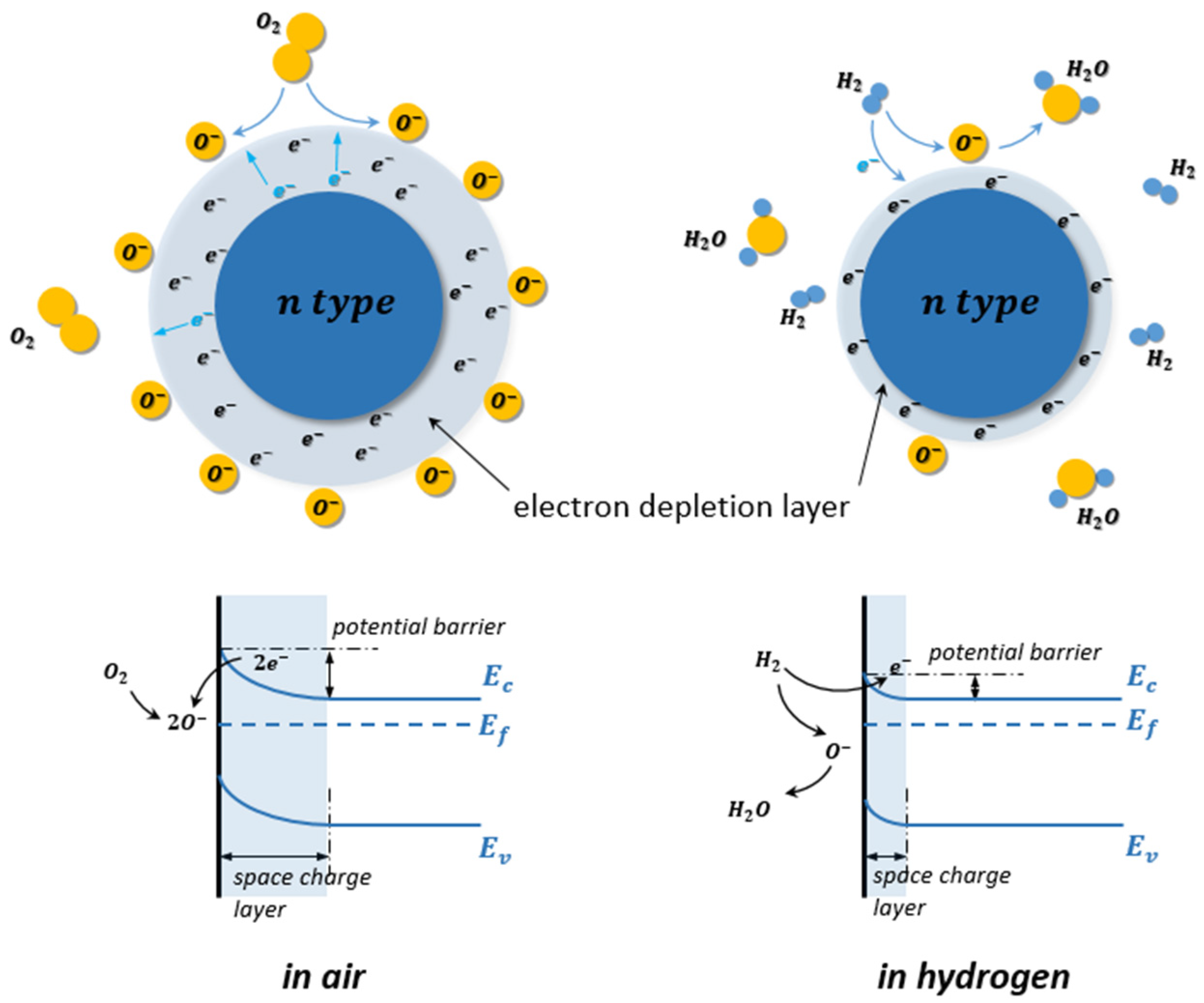
3. Metal Oxide Semiconductor-Based Hydrogen Gas Sensors
4. Graphene and Its Derivatives-Based Hydrogen Gas Sensors
4.1. Transition Metals/Graphene Combinations
4.2. Metal Oxide Semiconductor (MOS)/Graphene Combinations
5. Conclusions
- (1)
- Very high surface-to-volume ratio. Large exposed surfaces of sensing materials ensure a high density of defects for possible improvement of electron transfer, such as vacancies or dangling bonds. As reported in many works, certain optimized particle sizes can raise the sensing performance of the nanomaterial-based gas sensor;
- (2)
- The operating temperature of nanomaterials-based gas sensors is lower than traditional gas sensors based on bulk materials because of adsorption sites created by dangling bonds on the surface;
- (3)
- The unsatisfied bonds on the surface of nanosized materials also enable the surface functionalization and activation towards the target gas in sensing applications, which allows precise control and surface engineering methodologies to enhance the sensing performance in a wide range.
Author Contributions
Funding
Conflicts of Interest
References
- Adoption of the Paris Agreement, FCCC/CP/2015/L.9/Rev.1. UNFCCC Secretariat. Available online: https://unfccc.int/resource/docs/2015/cop21/eng/l09r01.pdf (accessed on 8 July 2021).
- Toyota. Mirai 2019 Electronic Brochure. Available online: https://www.toyota.com/content/ebrochure/2019/mirai_ebrochure.pdf (accessed on 8 July 2021).
- Hübert, T.; Boon-Brett, L.; Black, G.; Banach, U. Hydrogen sensors-a review. Sens. Actuators B Chem. 2011, 157, 329–352. [Google Scholar] [CrossRef]
- Hübert, T.; Boon-Brett, L.; Buttner, W.J. Hydrogen properties and technologies of its production and use. In Sensors for Safety and Process Control in Hydrogen Technologies; CRC Press: Boca Raton, FL, USA, 2016; pp. 12–15. ISBN 9781138894341. [Google Scholar]
- Buttner, W.; Burgess, R.; Post, M.; Rivikin, C. Summary and Findings from the NREL/DOE Hydrogen Sensor Workshop (8 June 2011); National Renewable Energy Lab (NREL): Golden, CO, USA, 2011. Available online: http://www.osti.gov/servlets/purl/1048994/ (accessed on 12 June 2021).
- Hydrogen and Fuel Cell Technologies Office Multi-Year Research, Development, and Demonstration Plan. Available online: https://www.energy.gov/eere/fuelcells/downloads/hydrogen-and-fuel-cell-technologies-office-multi-year-research-development (accessed on 25 July 2021).
- Buttner, W.J.; Post, M.B.; Burgess, R.; Rivkin, C. An overview of hydrogen safety sensors and requirements. Int. J. Hydrogen Energy 2011, 36, 2462–2470. [Google Scholar] [CrossRef]
- Penner, R.M. A nose for hydrogen gas: Fast, sensitive H2 sensors using electrodeposited nanomaterials. Acc. Chem. Res. 2017, 50, 1902–1910. [Google Scholar] [CrossRef]
- Yang, F.; Donavan, K.; Kung, S.C.; Penner, R.M. The surface scattering-based detection of hydrogen in air using a platinum nanowire. Nano Lett. 2012, 12, 2924–2930. [Google Scholar] [CrossRef] [PubMed]
- Deng, Y.H. Development of semiconducting metal oxide gas sensors. In Semiconducting Metal Oxides for Gas Sensing, 1st ed.; Hübert, T., Boon-Brett, L., Buttner, W.J., Eds.; Springer Nature Singapore Pte Ltd: Singapore, 2019; pp. 2–12. ISBN 978-981-13-5853-1. [Google Scholar]
- Fukai, Y. Atomistic states of hydrogen in metals. In The Metal-Hydrogen System: Basic Bulk Properties, 2nd ed.; Hull, R., Parisi, J., Jr., Osgood, R.M., Warlimont, H., Eds.; Springer Series in Materials Science; Springer: Berlin/Heidelberg, Germany, 2005; pp. 216–226. ISBN 978-3-540-28883-1. [Google Scholar]
- Li, J.; Hu, H.F.; Yao, C.B. Hydrogen sensing performance of silica microfiber elaborated with Pd nanoparticles. Mater. Lett. 2018, 212, 211–213. [Google Scholar] [CrossRef] [Green Version]
- Dekura, S.; Kobayashi, H.; Kusada, K.; Kitagawa, H. Hydrogen in palladium and storage properties of related nanomaterials: Size, shape, alloying, and metal-organic framework coating effects. ChemPhysChem 2019, 20, 1158–1176. [Google Scholar] [CrossRef] [PubMed] [Green Version]
- Nakatsuji, H.; Hada, M. Interaction of a hydrogen molecule with palladium. J. Am. Chem. Soc. 1985, 107, 8264–8266. [Google Scholar] [CrossRef]
- Bartczak, W.M.; Stawowska, J. Interaction of dihydrogen with transition metal (Pd, Ni, Ag, Cu) clusters. Struct. Chem. 2004, 15, 447–459. [Google Scholar] [CrossRef]
- Johnson, N.; Lam, B.; Macloed, B.P.; Sherbo, R.; Moreno-Gonzalez, M.; Fork, D.K.; Berlinguette, C.P. Facets and vertices regulate hydrogen uptake and release in palladium nanocrystals. Nat. Mater. 2019, 18, 454–458. [Google Scholar] [CrossRef]
- Nanba, Y.; Tsutsumi, T.; Ishimoto, T.; Koyama, M. Theoretical study of the hydrogen absorption mechanism into a palladium nanocube coated with a metal-organic framework. J. Phys. Chem. C 2017, 121, 14611–14617. [Google Scholar] [CrossRef] [Green Version]
- Grammatikkopoulos, P.; Cassidy, C.; Singh, V.; Sowwan, M. Coalescence-induced crystallisation wave in Pd nanoparticles. Sci. Rep. 2014, 4, 1–9. [Google Scholar] [CrossRef]
- Halgren, T.A.; Lipscomb, W.N. The synchronous-transit method for determining reaction pathways and locating molecular transition states. Chem. Phys. Lett. 1977, 49, 225–232. [Google Scholar] [CrossRef]
- Flanagen, T.B.; Oates, W.A. The palladium-hydrogen system. Annu. Rev. Mater. Sci. 1991, 21, 269–304. [Google Scholar] [CrossRef]
- Brian, D.A.; Chen, A.C. The role of palladium in hydrogen economy. Mater. Today 2011, 14, 282–289. [Google Scholar]
- Abens, P.C.; Burgers, W.G. Surface structure and electrochemical potential of palladium while adsorbing hydrogen in aqueous solution. Trans. Faraday Soc. 1962, 58, 1989–1992. [Google Scholar] [CrossRef]
- Lewis, F.A. The palladium-hydrogen system: A survey of hydride formation and effects of hydrogen contained within the metal lattices. Platin. Met. Rev. 1982, 26, 20–27. [Google Scholar]
- Frieske, H.; Wicke, E. Magnetic susceptibility and equilibrium diagram of PdHn. Ber. Bunsenges. Für Phys. Chem. 1973, 77, 48–52. [Google Scholar] [CrossRef]
- Akiba, H.; Kobayashi, H.; Kitagawa, H.; Kofu, M.; Yamamuro, O. Glass transition and positional ordering of hydrogen in bulk and nanocrystalline palladium. Phys. Rev. B 2015, 92, 064202. [Google Scholar] [CrossRef]
- Lässer, R.; Klatt, K.H. Solubility of hydrogen isotopes in palladium. Phys. Rev. B 1983, 28, 748. [Google Scholar] [CrossRef]
- Gupta, D.; Dutta, D.; Kumar, M.; Barman, P.B.; Sarkar, C.K.; Hazra, S.K. A low temperature hydrogen sensor based on palladium nanoparticles. Sens. Actuators B Chem. 2014, 196, 215–222. [Google Scholar] [CrossRef]
- Lee, E.; Lee, J.M.; Koo, J.H.; Lee, W.L.; Lee, T. Hysteresis behavior of electrical resistance in Pd thin films during the process of absorption and desorption of hydrogen gas. Int. J. Hydrogen Energy 2010, 35, 6984–6991. [Google Scholar] [CrossRef]
- Othonos, A.; Kalli, K.; Tsai, D.P. Optically thin palladium films on silicon-based substrates and nanostructure formation: Effects of hydrogen. Appl. Surf. Sci. 2000, 161, 54–60. [Google Scholar] [CrossRef]
- Dus, R.; Nowakowski, R.; Nowicka, E. Chemical and structural components of work function changes in the process of palladium hydride formation with thin Pd film. J. Alloy. Compd. 2005, 404, 284–287. [Google Scholar] [CrossRef]
- Ollagnier, A.; Fabre, A. Activation process of reversible Pd thin film hydrogen sensors. Sens. Actuators B 2013, 186, 258–262. [Google Scholar] [CrossRef]
- Sharma, B.; Yadav, H.M.; Kim, J.S. Multilayer thin film deposition of Pd/Ag alloy as an application for hydrogen. In Proceedings of the 2017 IEEE Sensors Applications Symposium (SAS), Glassboro, NJ, USA, 13–15 March 2017. [Google Scholar]
- Wang, W.; Liu, X.L.; Mei, S.C.; Liu, M.W.; Lu, C.; Lu, M.H. Development of a high stability Pd-Ni alloy thin-film coated SAW device for sensing hydrogen. Sensors 2019, 19, 3560. [Google Scholar] [CrossRef] [Green Version]
- Wadell, C.; Nugroho, F.A.A.; Lidström, E.; Landolo, B.; Wagner, J.B.; Langhammer, C. Hysteresis-free nanoplasmonic Pd-Au alloy hydrogen sensors. Nano Lett. 2015, 15, 3563–3570. [Google Scholar] [CrossRef]
- Yoshimura, K.; Nakano, S.; Uchinashi, S.; Yamaura, S.; Kimura, H.; Inoue, A. A hydrogen sensor based on Mg-Pd alloy thin film. Meas. Sci. Technol. 2007, 18, 3335–3338. [Google Scholar] [CrossRef]
- Zhao, M.; Wong, M.H.; Man, H.C.; Ong, C.W. Resistive hydrogen sensing response of Pd-decorated ZnO nanosponge film. Sens. Actuators B Chem. 2017, 249, 624–631. [Google Scholar] [CrossRef]
- Liu, Q.; Yao, J.Y.; Wang, Y.P.; Sun, Y.N.; Ding, G.F. Temperature dependent response/recovery characteristics of Pd/Ni thin film based hydrogen sensor. Sens. Actuator B. Chem. 2019, 290, 544–550. [Google Scholar] [CrossRef]
- Lee, E.; Lee, J.M.; Lee, E.; Noh, J.S.; Joe, J.H.; Jung, B.; Lee, W. Hydrogen gas sensing performance of Pd-Ni alloy thin films. Thin Solid Film 2010, 519, 880–884. [Google Scholar] [CrossRef]
- Viespe, C.; Miu, D. Surface acoustic wave sensor with Pd/ZnO bilayer structure for room temperature hydrogen detection. Sensors 2017, 17, 1529. [Google Scholar] [CrossRef]
- Song, H.; Chen, Y.P.; Gang, Z.; Liu, Y. Optical fiber hydrogen sensor based on an annealing-stimulated Pd-Y thin film. Sens. Actuators B Chem. 2015, 216, 11–16. [Google Scholar] [CrossRef]
- Deng, X.L.; Zhou, C.D.; Li, Z.L.; Cheng, K. Research about WO3/Pd film preparation for reflection type optical fiber hydrogen sensor. Appl. Mech. Mater. 2014, 563, 127–130. [Google Scholar] [CrossRef]
- Yamauchi, M.; Ikeda, R.; Kitagawa, H.; Takata, M. Nanosize effects on hydrogen storage in palladium. J. Phys. Chem. C 2008, 112, 3294–3299. [Google Scholar] [CrossRef]
- Bardhan, R.; Hedges, L.O.; Pint, C.L.; Javey, A.; Whitelam, S.; Urban, J.J. Uncovering the intrinsic size dependence of hydriding phase transformation in nanocrystals. Nat. Mater. 2013, 12, 905–912. [Google Scholar] [CrossRef] [PubMed] [Green Version]
- Sachs, C.; Pundt, A.; Kirchheim, R.; Winter, M.; Reetz, M.T.; Fritsch, D. Solubility of hydrogen in single-sized palladium cluster. Phys. Rev. B 2001, 64, 075408. [Google Scholar] [CrossRef]
- Stuhr, U.; Wipf, H.; Udovic, T.J.; Weissmuller, J.; Gleiter, H. The vibrational excitations and the position of hydrogen in nanocrystalline palladium. J. Phys. Condens. Matter 1995, 7, 219. [Google Scholar] [CrossRef]
- Stuhr, U.; Wipf, H.; Andersen, K.H.; Hahn, H. Neutron scattering study of the vibrational behaviour of H-doped nanocrystalline Pd. Phys. B Condens. Matter 2000, 276, 882–883. [Google Scholar] [CrossRef]
- Suleiman, M.; Jisrawi, N.M.; Dankert, O.; Reetz, M.T.; Bähtz, C.; Kirchheim, R.; Pundt, A. Phase transition and lattice expansion during hydrogen loading of nanometer sized palladium clusters. J. Alloy. Compd. 2003, 356, 644–648. [Google Scholar] [CrossRef]
- Eastman, J.; Thompson, L.J.; Kestel, J. Narrowing of the palladium-hydrogen miscibility gap in nanocrystalline palladium. Phys. Rev. B 1993, 48, 84. [Google Scholar] [CrossRef]
- Baldi, A.; Narayan, T.C.; Koh, A.L.; Dionne, J.A. In situ detection of hydrogen-induced phase transitions in individual palladium nanocrystals. Nat. Mater. 2014, 13, 1143–1148. [Google Scholar] [CrossRef]
- Griessen, R.; Strohfeldt, N.; Giessen, H. Thermodynamics of the hybrid interaction of hydrogen with palladium nanoparticles. Nat. Mater. 2016, 15, 311–317. [Google Scholar] [CrossRef]
- Griessen, R.; Feenstra, R. Volume changes during hydrogen absorption in metals. J. Phys. F Met. Phys. 1985, 15, 1013–1019. [Google Scholar] [CrossRef]
- Narayan, T.C.; Hayee, F.; Baldi, A.; Koh, A.L.; Sinclair, R.; Dionne, J.A. Direct visualization of hydrogen absorption dynamics in individual palladium nanoparticles. Nat. Commun. 2017, 8, 1–8. [Google Scholar] [CrossRef] [PubMed] [Green Version]
- Alefeld, G. Phase transitions of hydrogen in metals due to elastic interaction. Ber. Bunsenges. Für Phys. Chem. 1972, 76, 746–755. [Google Scholar]
- Wadell, C.; Pingel, T.; Olsson, E.; Zoric, L.; Zhdanov, V.P.; Langhammer, C. Thermodynamics of hydrogen formation and decomposition in supported sub-10nm Pd nanoparticles of different sizes. Chem. Phys. Lett. 2014, 603, 75–81. [Google Scholar] [CrossRef] [Green Version]
- Maxwell, J.C. On the dynamical evidence of the molecular constitution of bodies. Nature 1875, 11, 357–359. [Google Scholar] [CrossRef] [Green Version]
- Schwarz, R.B.; Khachaturyan, A.G. Thermodynamics of open two-phase systems with coherent interfaces. Phys. Rev. Lett. 1995, 74, 2523. [Google Scholar] [CrossRef]
- Schwarz, R.B.; Khachaturyan, A.G. Thermodynamics of open two-phase systems with coherent interfaces: Application to metal-hydrogen systems. Acta Mater. 2006, 54, 313–323. [Google Scholar] [CrossRef]
- Hu, Y.M.; Lei, J.M.; Wang, Z.; Yang, S.L. Rapid response hydrogen sensor based on nanoporous Pd thin films. Int. J. Hydrogen Energy 2016, 41, 10986–10990. [Google Scholar] [CrossRef] [Green Version]
- Liu, Q.; Yao, J.Y.; Wu, Y.J.; Wang, Y.P.; Ding, G.F. Two operating modes of palladium film hydrogen sensor based on suspended micro hotplate. Int. J. Hydrogen Energy 2019, 44, 11259–11265. [Google Scholar] [CrossRef]
- Mao, S.; Zhou, H.; Wu, S.H.; Yang, J.J.; Li, Z.Y.; Wei, X.B.; Wang, X.R.; Wang, Z.Y.; Li, J. High performance hydrogen sensor based on Pd/TiO2 composite film. Int. J. Hydrogen Energy 2018, 43, 22727–22732. [Google Scholar] [CrossRef]
- Xu, H.Y.; Liu, Y.J.; Liu, H.; Dong, S.C.; Wu, Y.P.; Wang, Z.G.; Wang, Y.M.; Wu, M.S.; Han, Z.D.; Hao, L.Z. Pd-decorated 2D SnSe ultrathin film on SiO2/Si for room-temperature hydrogen detection with ultrahigh response. J. Alloy. Compd. 2021, 851, 156844. [Google Scholar] [CrossRef]
- Pak, Y.; Lim, N.; Kumaresn, Y.; Lee, R.; Kim, K.; Kim, T.H.; Kim, S.M.; Ham, M.H.; Jung, G.Y. Palladium nanoribbon array for fast hydrogen gas sensing with ultrahigh sensitivity. Adv. Mater. 2015, 27, 6945–6952. [Google Scholar] [CrossRef]
- Hughes, R.C.; Schubert, W.K.; Zipperian, T.E.; Rodriguez, J.L.; Plut, T.A. Thin-film palladium and silver alloys and layers for metal-insulator-semiconductor sensors. J. Appl. Phys. 1987, 62, 1074–1083. [Google Scholar] [CrossRef]
- Du, L.L.; Feng, D.L.; Xing, X.X.; Fu, Y.; Fonsecs, L.F.; Yang, D.C. Palladium/cobalt nanowires with improved hydrogen sensing stability at ultra-low temperatures. Nanoscale 2019, 11, 21074–21080. [Google Scholar] [CrossRef]
- Yang, D.; Valentin, L.; Carpena, J.; Otano, W.; Resto, O.; Fonseca, L.F. Temperature-activated reverse sensing behavior of Pd nanowire hydrogen sensors. Small 2012, 9, 188–192. [Google Scholar] [CrossRef]
- Lee, J.S.; Seo, M.H.; Choi, K.W.; Yoo, J.Y.; Jo, M.S.; Yoon, J.B. Stress-engineered palladium nanowires for wide range (0.1%–3.9%) of H2 detection with high durability. Nanoscale 2019, 11, 16317–16326. [Google Scholar] [CrossRef]
- Ahn, J.H.; Yun, J.; Moon, D.I.; Choi, Y.K.; Park, I.K. Self-heated silicon nanowires for high performance hydrogen gas detection. Nanotechnology 2015, 26, 095501. [Google Scholar] [CrossRef] [PubMed]
- Lupan, O.; Postica, V.; Hoppe, M.; Wolff, N.; Polonsky, O.; Pauporte, T.; Viana, B.; Majerus, O.; Kienle, L.; Faupel, F.; et al. PdO/PdO2 functionalized ZnO : Pd films for lower operating temperature H2 gas sensing. Nanoscale 2018, 10, 14107–14127. [Google Scholar] [CrossRef]
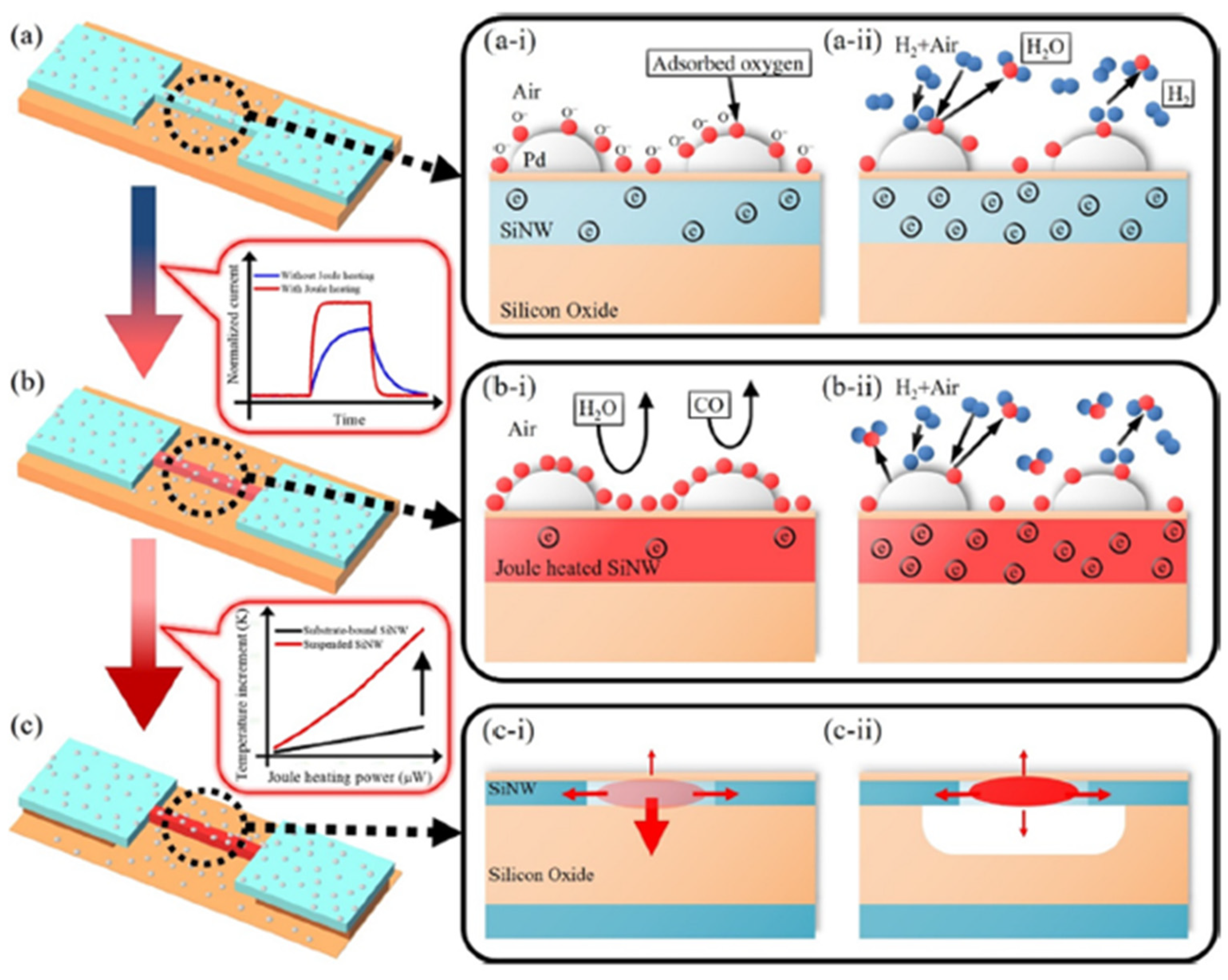
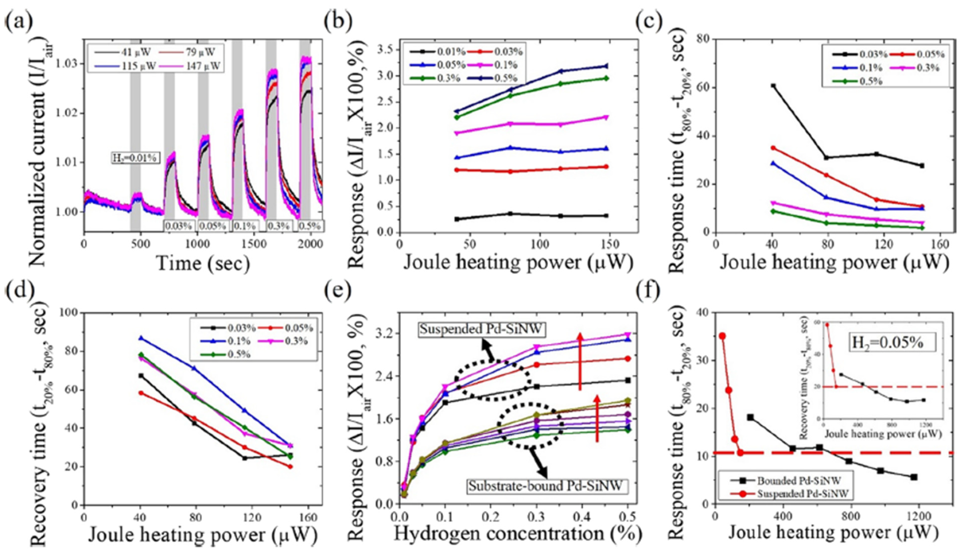
- Yun, J.; Ahn, J.H.; Moon, D.I.; Choi, Y.K.; Park, I.K. Joule-Heated and Suspended Silicon Nanowire Based Sensor for Low-Power and Stable Hydrogen Detection. ACS Appl. Mater. Interfaces 2019, 11, 42349–42357. [Google Scholar] [CrossRef] [PubMed]
- Offermans, P.; Tong, H.D.; van Riji, C.J.M.; Merken, P.; Brongersam, S.H.; Crego-Calama, M. Ultralow-power hydrogen sensing with single palladium nanowires. Appl. Phys. Lett. 2009, 94, 223110. [Google Scholar] [CrossRef]
- Yang, F.; Taggart, D.K.; Penner, R.M. Joule heating a palladium nanowire sensor for accelerated response and recovery to hydrogen gas. Small 2010, 6, 1422–1429. [Google Scholar] [CrossRef] [PubMed]
- Cho, M.; Zhu, J.X.; Kim, H.; Kang, K.; Park, I.K. Half-pipe palladium nanotube-based hydrogen sensor using a suspended nanofiber scaffold. ACS Appl. Mater. Interfaces 2019, 11, 13343–13349. [Google Scholar] [CrossRef] [PubMed]
- Wang, W.; Liu, X.L.; Mei, S.C.; Jia, Y.N.; Liu, M.W.; Xue, X.F.; Yang, D.C. Development of a Pd/Cu nanowires coated SAW hydrogen gas sensor with fast response and recovery. Sens. Actuators B Chem. 2019, 287, 157–164. [Google Scholar] [CrossRef]
- Baek, J.; Jang, B.J.; Kim, M.H.; Kim, W.; Kim, J.; Rim, H.J.; Shin, S.; Lee, T.; Cho, S.; Lee, W.Y. High-performance hydrogen sensing properties and sensing mechanism in Pd-coated p-type Si nanowire arrays. Sens. Actuators B Chem. 2017, 256, 465–471. [Google Scholar] [CrossRef]
- Koo, W.; Qiao, S.P.; Ogata, A.F.; Jha, G.; Jang, J.S.; Chen, V.T.; Kim, I.D.; Penner, R.M. Accelerating palladium nanowire H2 sensors using engineered nanofiltration. ACS Nano 2017, 11, 9276–9285. [Google Scholar] [CrossRef]
- Zheng, L.J.; Zheng, S.Z.; Wei, H.R.; Du, L.L.; Zhu, Z.Y.; Chen, J.; Yang, D.C. Palladium/Bismuth/Copper hierarchical nano-architectures for efficient hydrogen evolution and stable hydrogen detection. ACS Appl. Mater. Interfaces 2019, 11, 6248–6256. [Google Scholar] [CrossRef]
- Wang, F.P.; Hu, K.L.; Liu, H.C.; Zhao, Q.; Wang, K.Z.; Zhang, Y.X. Low temperature and fast response hydrogen gas sensor with Pd coated SnO2 nanofiber rods. Int. J. Hydrogen Energy 2020, 45, 7234–7242. [Google Scholar] [CrossRef]
- Kumar, R.; Malik, S.; Mehta, B.R. Interface induced hydrogen sensing in Pd nanoparticle/graphene composite layers. Sens. Actuators B Chem. 2015, 209, 919–926. [Google Scholar] [CrossRef]
- Behzadi Pour, G.; Fekri Aval, L. Comparison of fast response and recovery Pd nanoparticles and Ni thin film hydrogen gas sensors based on metal-oxide-semiconductor structure. Nano 2017, 12, 1750096. [Google Scholar] [CrossRef]
- Bentarzi, H. The MOS structure. In Transport in Metal-Oxide-Semiconductor Structure: Mobile Ions Effects on the Oxide Properties; Springer: Berlin/Heidelberg, Germany, 2011; pp. 5–11. ISBN 978-3-642-16304-3. [Google Scholar]
- Kumar, M.P.; Logesh, K.; Dutta, S. Limitations of Mott-Schottky analysis for organic metal-insulator-semiconductor capacitors. In The Physics of Semiconductor Devices, 1st ed.; Sharma, R.K., Rawal, D.S., Eds.; Springer Nature Switzerland AG: Cham, Switzerland, 2019; pp. 69–74. ISBN 978-0-470-06832-8. [Google Scholar]
- Chen, M.R.; Mao, P.; Qin, Y.Y.; Wang, J.; Xie, B.; Wang, X.Z.; Han, D.Y.; Wang, G.H.; Song, F.Q.; Han, M.; et al. Response characteristics of hydrogen sensors based on PMMA-membrane-coated palladium nanoparticle films. ACS Appl. Mater. Interfaces 2017, 9, 27193–27201. [Google Scholar] [CrossRef]
- Hulme, J.; Komaki, M.; Nishimura, C.; Gwak, J. The effect of gas mixtures on hydrogen permeation through Pd-Ag/V-Ni alloy composite membrane. Curr. Appl. Phys. 2011, 11, 972–975. [Google Scholar] [CrossRef]
- Miguel, C.V.; Mendes, A.; Tosti, S.; Madeira, M. Effect of CO and CO2 on H2 permeation through finger-like Pd-Ag membranes. Int. J. Hydrogen Energy 2012, 37, 12680–12687. [Google Scholar] [CrossRef]
- Hong, J.; Lee, S.; Seo, J.; Pyo, S.; Kim, J.; Lee, T. A highly sensitive hydrogen sensor with gas selectivity using a PMMA membrane-coated Pd nanoparticle/single-layer graphene hybrid. ACS Appl. Mater. Interfaces 2015, 7, 3554–3561. [Google Scholar] [CrossRef] [PubMed]
- Rashid, T.R.; Phan, D.T.; Chung, G.S. Effect of Ga-modified layer on flexible hydrogen sensor using ZnO nanorods decorated by Pd catalysts. Sens. Actuators B 2014, 193, 869–876. [Google Scholar] [CrossRef]
- Li, Y.X.; Deng, D.Y.; Chen, N.; Xing, X.X.; Liu, X.; Xiao, X.C.; Wang, Y.D. Pd nanoparticles composited SnO2 microspheres as sensing materials for gas sensors with enhanced hydrogen response performances. J. Alloy. Compd. 2017, 710, 216–224. [Google Scholar] [CrossRef]
- Kim, J.H.; Mirzael, A.; Kim, H.W.; Kim, S.S. Improving the hydrogen sensing properties of SnO2 nanowires-based conductometric sensors by Pd-decoration. Sens. Actuators B Chem. 2019, 285, 358–367. [Google Scholar] [CrossRef]
- Annanouch, F.E.; Roso, S.; Haddi, Z.; Vallejos, S.; Blackmann, C.; Vilic, T.; Llobet, E. p-Type PdO nanoparticles supported on n-type WO3 nanoneedles for hydrogen sensing. Thin Solid Films 2016, 618, 238–245. [Google Scholar] [CrossRef]
- Wang, Z.H.; Huang, S.N.; Men, G.L.; Han, D.M.; Gu, F.B. Sensitization of Pd loading for remarkably enhanced hydrogen sensing performance of 3DOM WO3. Sens. Actuators B 2018, 262, 577–587. [Google Scholar] [CrossRef]
- Sanger, A.; Kumar, A.; Kumar, A.; Chandra, R. Highly sensitive and selective hydrogen gas sensor using sputtered grown Pd decorated MnO2 nanowalls. Sens. Actuators B 2016, 234, 8–14. [Google Scholar] [CrossRef]
- Baek, D.H.; Kim, J. MoS2 gas sensor functionalized by Pd for the detection of hydrogen. Sens. Actuators B Chem. 2017, 250, 686–691. [Google Scholar] [CrossRef]
- Weber, M.; Kim, J.Y.; Lee, J.H.; Kim, J.H.; Iatsunskyi, I.; Coy, E.; Miele, P.; Bechelany, M.; Kim, S.S. Highly efficient hydrogen sensors based on Pd nanoparticles supported on boron nitride coated ZnO nanowires. J. Mater. Chem. A 2019, 7, 8107–8116. [Google Scholar] [CrossRef]
- Gao, L.J.; Fu, Q.; Wei, M.M.; Zhu, Y.F.; Liu, Q.; Crumlin, E.; Liu, Z.; Bao, X.H. Enhanced nickel catalyzed methanation confined under hexagonal boron nitride Shells. ACS Catal. 2016, 6, 6814–6822. [Google Scholar] [CrossRef]
- Weber, M.; Lamboux, C.; Navarra, B.; Miele, P.; Zanna, S.; Dufond, M.E.; Santinacci, L.; Bechelany, M. Boron nitride as a novel support for highly stable palladium nanocatalysts by atomic layer deposition. Nanomaterials 2018, 8, 849. [Google Scholar] [CrossRef] [PubMed] [Green Version]
- Ganose, A.M.; Scanlon, D.O. Band gap and work function tailoring of SnO2 for improved transparent conducting ability in photovoltaics. J. Mater. Chem. C 2016, 4, 1467–1475. [Google Scholar] [CrossRef] [Green Version]
- Guo, Y.; Ma, L.; Mao, K.K.; Ju, M.G.; Bai, Y.Z.; Zhao, J.J.; Zeng, X.C. Eighteen functional monolayer metal oxides: Wide bandgap semiconductors with superior oxidation resistance and ultrahigh carrier mobility. Nanoscale Horiz. 2019, 4, 592–600. [Google Scholar] [CrossRef] [Green Version]
- Deng, Y.H. Sensors for environmental gases. In Semiconducting Metal Oxides for Gas Sensing; Springer: Singapore, 2019; pp. 209–216. ISBN 978-981-13-5853-1. [Google Scholar]
- Nakate, U.T.; Lee, G.H.; Ahmad, R.; Patil, P.; Bhopate, D.P.; Hahn, Y.B.; Yu, Y.T.; Suh, E.K. Hydrothermal synthesis of p-type nanocrystalline NiO nanoplates for high response and low concentration hydrogen gas sensor application. Ceram. Int. 2018, 44, 15721–15729. [Google Scholar] [CrossRef]
- Zhang, J.; Qin, Z.Y.; Zeng, D.W.; Xie, C.S. Metal-oxide-semiconductor based gas sensors: Screening, preparation, and integration. Phys. Chem. Chem. Phys. 2017, 19, 6313–6329. [Google Scholar] [CrossRef]
- Barsan, N.; Weimar, U. Conduction model of metal oxide gas sensors. J. Electroceram. 2001, 7, 143–167. [Google Scholar] [CrossRef]
- Min, B.K.; Friend, C.M. Heterogeneous gold-based catalysis for green chemistry: Low-temperature CO oxidation and propene oxidation. Chem. Rev. 2007, 107, 2709–2724. [Google Scholar] [CrossRef] [PubMed]
- Kim, H.J.; Lee, J.H. Highly sensitive and selective gas sensors using p-type oxide semiconductors: Overview. Sens. Actuators B Chem. 2014, 192, 607–627. [Google Scholar] [CrossRef]
- Barsan, N.; Simion, C.; Heine, T.; Pokhrel, S.; Weimar, U. Modeling of sensing and transduction for p-type semiconducting metal oxide based gas sensors. J. Electroceram. 2010, 25, 11–19. [Google Scholar] [CrossRef]
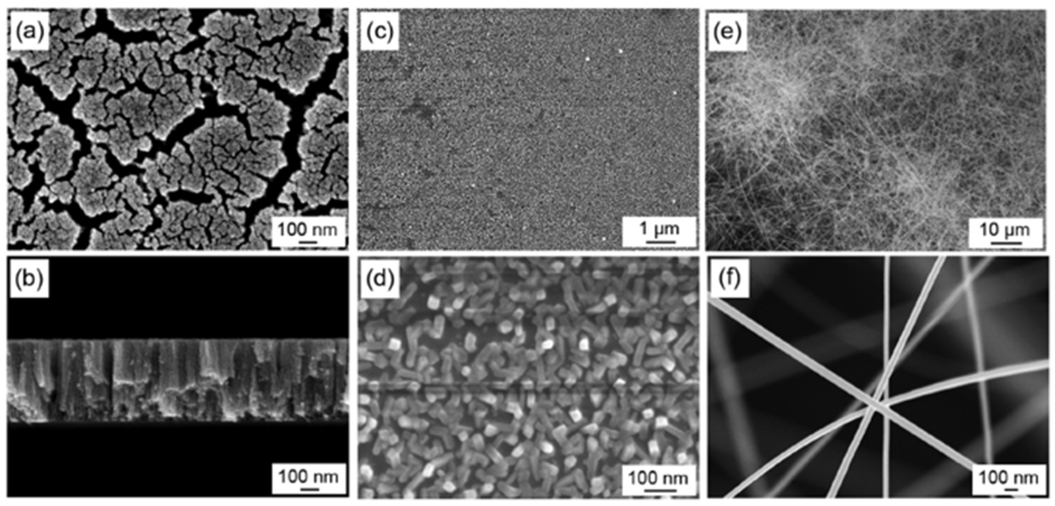
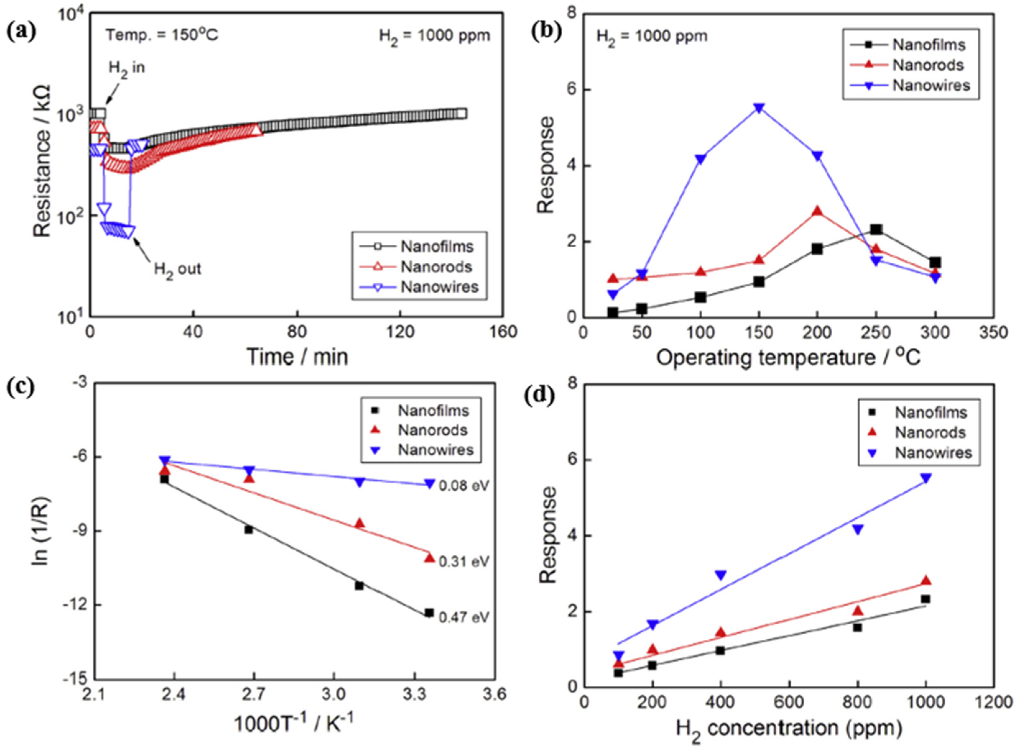
- Shen, Y.B.; Wang, W.; Fan, A.F.; Wei, D.Z.; Liu, W.G.; Han, C.; Shen, Y.S.; Meng, D.; San, X.G. Highly sensitive hydrogen sensors based on SnO2 nanomaterials with different morphologies. Int. J. Hydrogen Energy 2015, 40, 15773–15779. [Google Scholar] [CrossRef]
- Zhu, L.; Zeng, W.; Li, Y.Q. A non-oxygen adsorption mechanism for hydrogen detection of nanostructured SnO2 based sensors. Mater. Res. Bull. 2019, 109, 108–116. [Google Scholar] [CrossRef]
- Krishnakumar, T.; Kiruthiga, A.; Jozwiak, E.; Moulaee, K.; Neri, G. Development of ZnO-based sensors for fuel cell cars equipped with ethanol steam-reformer for on-board hydrogen production. Ceram. Int. 2020, 46, 17076–17084. [Google Scholar] [CrossRef]
- Hübert, T.; Boon-Brett, L.; Buttner, W.J. Hydrogen Sensors. In Sensors for Safety and Process Control in Hydrogen Technologies; CRC Press: Boca Raton, FL, USA, 2018; pp. 101–110. ISBN 978-1-4665-9655-9. [Google Scholar]
- Lavanya, N.; Sekar, C.; Fazio, E.; Neri, F.; Leonardi, S.G.; Neri, G. Development of a selective hydrogen leak sensor based on chemically doped SnO2 for automotive applications. Int. J. Hydrogen Energy 2017, 42, 10645–10655. [Google Scholar] [CrossRef]
- Korotcenkov, G.; Cho, B.K. Ozone measuring: What can limit application of SnO2-based conductometric gas sensors? Sens. Actuators B Chem. 2012, 161, 28–44. [Google Scholar] [CrossRef]
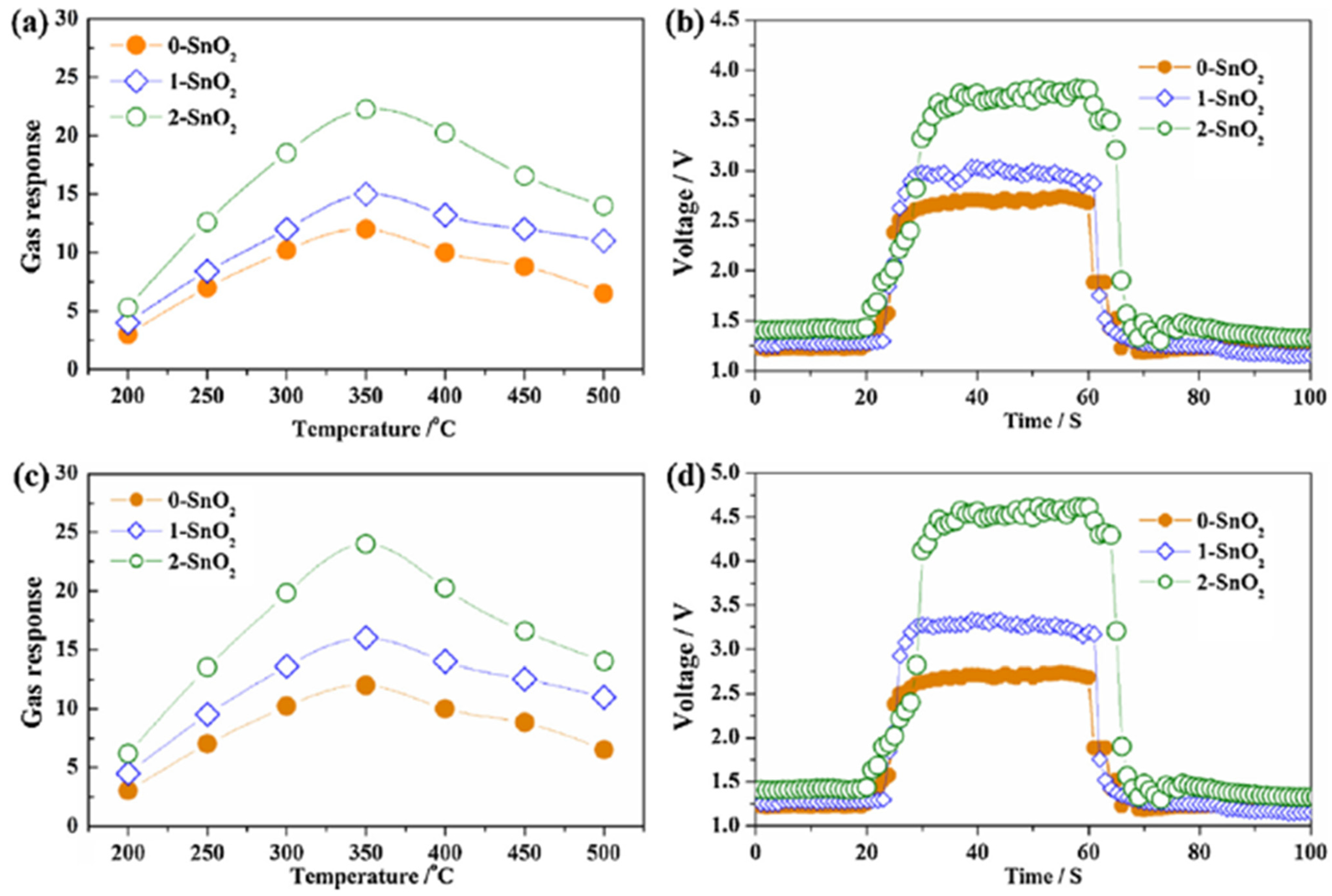
- Liu, G.; Wang, Z.; Chen, Z.H.; Yang, S.L.; Fu, X.X.; Huang, R.; Li, X.K.; Xiong, J.; Hu, Y.M.; Gu, H.S. Remarkably enhanced room-temperature hydrogen sensing of SnO2 nanoflowers via vacuum annealing treatment. Sensors 2018, 18, 949. [Google Scholar] [CrossRef] [Green Version]
- Yang, L.; Yin, C.B.; Zhang, Z.L.; Zhou, J.J.; Xu, H.H. The investigation of hydrogen gas sensing properties of SAW gas sensor based on palladium surface modified SnO2 thin film. Mater. Sci. Semicond. Process. 2017, 60, 16–28. [Google Scholar] [CrossRef]
- Chen, Z.H.; Hu, K.Y.; Yang, P.Y.; Fu, X.X.; Wang, Z.; Yang, S.L.; Xiong, J.; Zhang, X.H.; Hu, Y.M.; Gu, H.S. Hydrogen sensors based on Pt-decorated SnO2 nanorods with fast and sensitive room-temperature sensing performance. J. Alloy. Compd. 2019, 811, 152086. [Google Scholar] [CrossRef]
- Yin, X.T.; Zhou, W.D.; Li, J.; Wang, Q.; Wu, F.Y.; Dastan, D.; Wang, D.; Garmestani, H.; Wang, X.M.; Ţălu, Ş. A highly sensitivity and selectivity Pt-SnO2 nanoparticles for sensing applications at extremely low level hydrogen gas detection. J. Alloy. Compd. 2019, 805, 229–236. [Google Scholar] [CrossRef]
- Wang, Y.; Zhao, Z.T.; Sun, Y.J.; Li, P.W.; Ji, J.L.; Chen, Y.; Zhang, W.D.; Hu, J. Fabrication and gas sensing properties of Au-loaded SnO2 composite nanoparticles for highly sensitive hydrogen detection. Sens. Actuators B Chem. 2017, 240, 664–673. [Google Scholar] [CrossRef]
- Abdulah, Q.N.; Yam, F.K.; Hassan, Z.; Bououdina, M. Hydrogen gas sensing performance of GaN nanowires-based sensor at low operating temperature. Sens. Actuators B Chem. 2014, 204, 497–506. [Google Scholar] [CrossRef]
- Ma, S.Y.; Hu, M.; Zeng, P.; Li, M.D.; Yan, W.J.; Qin, Y.X. Synthesis and low-temperature gas sensing properties of tungsten oxide nanowires/porous silicon composite. Sens. Actuators B Chem. 2014, 192, 341–349. [Google Scholar] [CrossRef]
- Gurlo, A. Nanosensors: Towards morphological control of gas sensing activity. SnO2, In2O3, ZnO and WO3 case studies. Nanoscale 2011, 3, 154–165. [Google Scholar] [CrossRef]
- Yu, H.; Yang, T.Y.; Wang, Z.Y.; Li, Z.F.; Xiao, B.X.; Zhao, Q.; Zhang, M.Z. Facile synthesis cedar-like SnO2 hierarchical micro-nanostructures with improved formaldehyde gas sensing characteristics. J. Alloy. Compd. 2017, 724, 121–129. [Google Scholar] [CrossRef]
- Yang, W.H.; Lu, W.C.; Xue, X.Y.; Zang, Q.J. A theoretical study on CO sensing mechanism of In-doped SnO2 (1 1 0) surface. Comput. Theor. Chem. 2015, 1069, 119–124. [Google Scholar] [CrossRef]
- Vallejos, S.; Gràcia, I.; Lednický, T.; Vojkuvka, L.; Figueras, E.; Hubálek, J.; Cané, C. Highly hydrogen sensitive micromachined sensors based on aerosol-assisted chemical vapor deposited ZnO rods. Sens. Actuators B Chem. 2018, 268, 15–21. [Google Scholar] [CrossRef]
- Kim, J.H.; Mirzaei, A.; Osada, M.; Kim, H.W.; Kim, S.S. Hydrogen sensing characteristics of Pd-decorated ultrathin ZnO nanosheets. Sens. Actuators B Chem. 2021, 329, 129222. [Google Scholar] [CrossRef]
- Hu, K.L.; Wang, F.P.; Shen, Z.J.; Liu, H.C.; Zeng, W.; Wang, Y. Ar plasma treatment on ZnO–SnO2 heterojunction nanofibers and its enhancement mechanism of hydrogen gas sensing. Ceram. Int. 2020, 46, 21439–21447. [Google Scholar] [CrossRef]
- Jang, S.; Jung, S.; Baik, K.H. Hydrogen sensing performance of ZnO Schottky diodes in humid ambient conditions with PMMA membrane layer. Sensors 2020, 20, 835. [Google Scholar] [CrossRef] [Green Version]
- Nakate, U.T.; Ahmad, R.; Patil, P.; Bhat, K.S.; Wang, Y.S.; Mahmoudi, T.; Yu, Y.T.; Suh, E.K.; Hahn, Y.B. High response and low concentration hydrogen gas sensing properties using hollow ZnO particles transformed from polystyrene@ ZnO core-shell structures. Int. J. Hydrogen Energy 2019, 44, 15677–15688. [Google Scholar] [CrossRef]
- Kim, J.H.; Mirzaei, A.; Kim, H.W.; Kim, S.S. Combination of Pd loading and electron beam irradiation for superior hydrogen sensing of electrospun ZnO nanofibers. Sens. Actuators B Chem. 2019, 284, 628–637. [Google Scholar] [CrossRef]
- Lee, J.H.; Kim, J.Y.; Kim, J.H.; Kim, S.S. Enhanced hydrogen detection in ppb-level by electrospun SnO2-loaded ZnO nanofibers. Sensors 2019, 19, 726. [Google Scholar] [CrossRef] [PubMed] [Green Version]
- Krško, O.; Plecenik, T.; Roch, T.; Grančič, B.; Satrapinskyy, L.; Truchlý, M.; Ďurina, P.; Gregor, M.; Kúš, P.; Plecenik, A. Flexible highly sensitive hydrogen gas sensor based on a TiO2 thin film on polyimide foil. Sens. Actuators B Chem. 2017, 240, 1058–1065. [Google Scholar] [CrossRef]
- Chen, W.P.; Xiong, Y.; Li, Y.S.; Cui, P.; Guo, S.S.; Chen, W.; Tang, Z.L.; Yan, Z.J.; Zhang, Z.Y. Extraordinary room-temperature hydrogen sensing capabilities of porous bulk Pt–TiO2 nanocomposite ceramics. Int. J. Hydrogen Energy 2016, 41, 3307–3312. [Google Scholar] [CrossRef]
- Herrmann, J.M.; Pichat, P. Metal-support interactions: An in situ electrical conductivity study of Pt/TiO2 catalysts. J. Catal. 1982, 78, 425–435. [Google Scholar] [CrossRef]
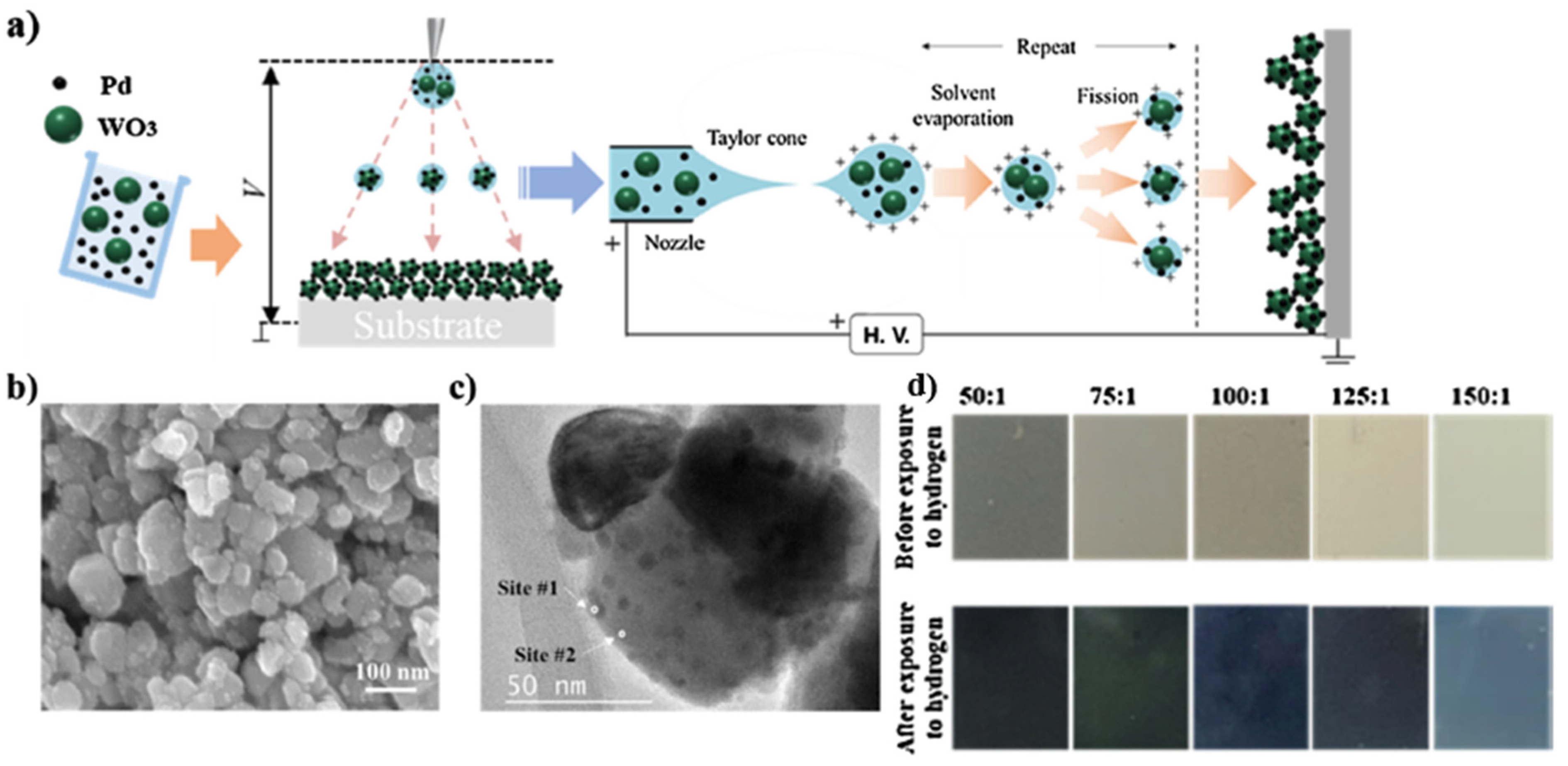
- Lee, J.; Koo, H.; Kim, S.Y.; Kim, S.J.; Lee, W. Electrostatic spray deposition of chemochromic WO3-Pd sensor for hydrogen leakage detection at room temperature. Sens. Actuators B Chem. 2021, 327, 128930. [Google Scholar] [CrossRef]
- Watanabe, T.; Okazaki, S.; Nakagawa, H.; Murata, K.; Fukuda, K. A fiber-optic hydrogen gas sensor with low propagation loss. Sens. Actuators B Chem. 2010, 145, 781–787. [Google Scholar] [CrossRef]
- Boudiba, A.; Roussel, P.; Zhang, C.; Olivier, M.G.; Snyders, R.; Debliquy, M. Sensing mechanism of hydrogen sensors based on palladium-loaded tungsten oxide (Pd–WO3). Sens. Actuators B Chem. 2013, 187, 84–93. [Google Scholar] [CrossRef]
- Liu, B.; Cai, D.P.; Liu, Y.; Wang, D.D.; Wang, L.L.; Wang, Y.R.; Li, H.; Li, Q.H.; Wang, T.H. Improved room-temperature hydrogen sensing performance of directly formed Pd/WO3 nanocomposite. Sens. Actuators B Chem. 2014, 193, 28–34. [Google Scholar] [CrossRef]
- Saenger, M.F.; Höing, T.; Robertson, B.W.; Billa, R.B.; Hofmann, T.; Schubert, E.; Schubert, M. Polaron and phonon properties in proton intercalated amorphous tungsten oxide thin films. Phys. Rev. B 2008, 78, 245205. [Google Scholar] [CrossRef] [Green Version]
- Zhou, X.; Dai, Y.T.; Karanja, J.M.; Liu, F.F.; Yang, M.H. Microstructured FBG hydrogen sensor based on pt-loaded WO3. Opt. Express 2017, 25, 8777–8786. [Google Scholar] [CrossRef] [PubMed]
- Caucheteur, C.; Debliquy, M.; Lahem, D.; Mégret, P. Catalytic fiber Bragg grating sensor for hydrogen leak detection in air. IEEE Photon. Technol. Lett. 2008, 20, 96–98. [Google Scholar] [CrossRef]
- Geim, A.K.; Novoselov, K.S. The rise of graphene. In Nanoscience and Technology: A Collection of Reviews from Nature Journals; Rodgers, P., Ed.; World Scientific: Singapore, 2010; pp. 11–19. ISBN 10-981-4282-68-5. [Google Scholar]
- Magne, S.; Rougeault, S.; Vilela, M.; Ferdinand, P. State-of-strain evaluation with fiber Bragg grating rosettes: Application to discrimination between strain and temperature effects in fiber sensors. Appl. Opt. 1997, 36, 9437–9447. [Google Scholar] [CrossRef]
- Katoch, A.; Kim, J.H.; Kwon, Y.J.; Kim, H.W.; Kim, S.S. Bifunctional sensing mechanism of SnO2–ZnO composite nanofibers for drastically enhancing the sensing behavior in H2 gas. ACS Appl. Mater. Interfaces 2015, 7, 11351–11358. [Google Scholar] [CrossRef]
- Lee, J.H.; Kim, J.H.; Kim, J.Y.; Mirzaei, A.; Kim, H.W.; Kim, S.S. ppb-Level selective hydrogen gas detection of Pd-functionalized In2O3-loaded ZnO nanofiber gas sensors. Sensors 2019, 19, 4276. [Google Scholar] [CrossRef] [Green Version]
- Novoselov, K.S.; Geim, A.K.; Morozov, S.V.; Jiang, D.E.; Zhang, Y.; Dubonos, S.V.; Grigorieva, I.V.; Firsov, A.A. Electric field effect in atomically thin carbon films. Science 2004, 306, 666–669. [Google Scholar] [CrossRef] [Green Version]
- Novoselov, K.S.; Geim, A.K.; Morozov, S.V.; Jiang, D.; Katsnelson, M.I.; Grigorieva, I.V.; Dubonos, S.V.; Firsov, A.A. Two-dimensional gas of massless Dirac fermions in graphene. Nature 2005, 438, 197–200. [Google Scholar] [CrossRef]
- Emtsev, K.V.; Bostwick, A.; Horn, K.; Jobst, J.; Kellogg, G.L.; Ley, L.; McChesney, J.L.; Ohta, T.; Reshanov, S.A.; Röhrl, J.; et al. Towards wafer-size graphene layers by atmospheric pressure graphitization of silicon carbide. Nat. Mater. 2009, 8, 203–207. [Google Scholar] [CrossRef] [PubMed]
- Dan, Y.P.; Lu, Y.; Kybert, N.J.; Luo, Z.T.; Johnson, A.T.C. Intrinsic response of graphene vapor sensors. Nano Lett. 2009, 9, 1472–1475. [Google Scholar] [CrossRef] [Green Version]
- Morozov, S.V.; Novoselov, K.S.; Katsnelson, M.I.; Schedin, F.; Elias, D.C.; Jaszczak, J.A.; Geim, A.K. Giant intrinsic carrier mobilities in graphene and its bilayer. Phys. Rev. Lett. 2008, 100, 016602. [Google Scholar] [CrossRef] [Green Version]
- Wu, Z.S.; Ren, W.C.; Wen, L.; Gao, L.B.; Zhao, J.P.; Chen, Z.P.; Zhou, G.M.; Li, F.; Cheng, H.M. Graphene anchored with Co3O4 nanoparticles as anode of lithium ion batteries with enhanced reversible capacity and cyclic performance. ACS Nano 2010, 4, 3187–3194. [Google Scholar] [CrossRef]
- Ma, L.P.; Wu, Z.S.; Li, J.; Wu, E.D.; Ren, W.C.; Cheng, H.M. Hydrogen adsorption behavior of graphene above critical temperature. Int. J. Hydrogen Energy 2009, 34, 2329–2332. [Google Scholar] [CrossRef]
- Sehrawat, P.; Islam, S.S.; Mishra, P.; Ahmad, S. Reduced graphene oxide (rGO) based wideband optical sensor and the role of temperature, defect states and quantum efficiency. Sci. Rep. 2018, 8, 1–13. [Google Scholar]
- Shahriary, L.; Athawale, A.A. Graphene oxide synthesized by using modified hummers approach. Int. J. Energy Environ. Eng. 2014, 2, 58–63. [Google Scholar]
- Dreyer, D.R.; Park, S.J.; Bielawski, C.W.; Ruoff, R.S. The chemistry of graphene oxide. Chem. Soc. Rev. 2010, 39, 228–240. [Google Scholar] [CrossRef]
- Wang, X.; Li, X.; Zhao, Y.; Chen, Y.; Yu, J.; Wang, J. The influence of oxygen functional groups on gas-sensing properties of reduced graphene oxide (rGO) at room temperature. RSC Adv. 2016, 6, 52339–52346. [Google Scholar] [CrossRef]
- Choi, Y.R.; Yoon, Y.G.; Choi, K.S.; Kang, J.H.; Shim, Y.S.; Kim, Y.H.; Jang, H.W. Role of oxygen functional groups in graphene oxide for reversible room-temperature NO2 sensing. Carbon 2015, 91, 178–187. [Google Scholar] [CrossRef]
- Tian, H.; Yang, Y.; Xie, D.; Cui, Y.L.; Mi, W.T.; Zhang, Y.; Ren, T.L. Wafer-scale integration of graphene-based electronic, optoelectronic and electroacoustic devices. Sci. Rep. 2014, 4, 1–9. [Google Scholar] [CrossRef] [PubMed] [Green Version]
- Mattson, E.C.; Johns, J.E.; Pande, K.; Bosch, R.A.; Cui, S.; Gajdardziska-Josifovska, M.; Weinert, M.; Chen, J.H.; Hersam, M.C.; Hirschmugl, C.J. Vibrational excitations and low-energy electronic structure of epoxide-decorated graphene. J. Phys. Chem. Lett. 2014, 5, 212–219. [Google Scholar] [CrossRef] [Green Version]
- Liang, H. Mid-infrared response of reduced graphene oxide and its high-temperature coefficient of resistance. AIP Adv. 2014, 4, 107131. [Google Scholar] [CrossRef] [Green Version]
- Shao, Z.C.; Hayasaka, T.; Liu, H.L.; Liang, J.M.; Wu, Y.C.; Lin, L.W. Crumpled and stretchable graphene gas sensor with enhanced sensitivity to hydrogen. In Proceedings of the 2019 IEEE 32nd International Conference on Micro Electro Mechanical Systems (MEMS), Seoul, Korea, 27–31 January 2019; pp. 145–148. [Google Scholar]
- Celebi, K.; Buchheim, J.; Wyss, R.M.; Droudian, A.; Gasser, P.; Shorubalko, I.; Kye, J.; Lee, C.; Park, H.G. Ultimate permeation across atomically thin porous graphene. Science 2014, 344, 289–292. [Google Scholar] [CrossRef] [PubMed]
- Shaban, M.; Ali, S.; Rabia, M. Design and application of nanoporous graphene oxide film for CO2, H2, and C2H2 gases sensing. J. Mater. Res. Technol. 2019, 8, 4510–4520. [Google Scholar] [CrossRef]
- Wang, J.W.; Singh, B.; Maeng, S.; Joh, H.I.; Kim, G.H. Assembly of thermally reduced graphene oxide nanostructures by alternating current dielectrophoresis as hydrogen-gas sensors. Appl. Phys. Lett. 2013, 103, 083112. [Google Scholar] [CrossRef]
- Johnson, J.L.; Behnam, A.; Pearton, S.J.; Ural, A. Hydrogen sensing using Pd-functionalized multi-layer graphene nanoribbon networks. Adv. Mater. 2010, 22, 4877–4880. [Google Scholar] [CrossRef] [PubMed]
- Tang, X.H.; Haddad, P.A.; Mager, N.; Geng, X.; Reckinger, N.; Hermans, S.; Debliquy, M.; Paskin, J.P. Chemically deposited palladium nanoparticles on graphene for hydrogen sensor applications. Sci. Rep. 2019, 9, 1–11. [Google Scholar]
- Ma, J.; Zhou, Y.L.; Bai, X.; Chen, K.; Guan, B.O. High-sensitivity and fast-response fiber-tip Fabry–Pérot hydrogen sensor with suspended palladium-decorated graphene. Nanoscale 2019, 11, 15821–15827. [Google Scholar] [CrossRef]
- Yokoyama, T.; Tanaka, T.; Shimokawa, Y.; Yamachi, R.; Saito, Y.; Uchida, K. Pd-functionalized, suspended graphene nanosheet for fast, low-energy multimolecular sensors. ACS Appl. Nano Mater. 2018, 1, 3886–3894. [Google Scholar] [CrossRef]
- Sharma, B.; Kim, J.S. MEMS based highly sensitive dual FET gas sensor using graphene decorated Pd-Ag alloy nanoparticles for H2 detection. Sci. Rep. 2018, 8, 1–9. [Google Scholar] [CrossRef]
- Zhang, M.; Brooks, L.L.; Chartuprayoon, N.; Bosze, W.; Choa, Y.H.; Myung, N.V. Palladium/single-walled carbon nanotube back-to-back Schottky contact-based hydrogen sensors and their sensing mechanism. ACS Appl. Mater. Interfaces 2014, 6, 319–326. [Google Scholar] [CrossRef]
- Yu, Y.J.; Zhao, Y.R.; Ryu, S.; Brus, L.E.; Kim, K.S.; Kim, P. Tuning the graphene work function by electric field effect. Nano Lett. 2009, 9, 3430–3434. [Google Scholar] [CrossRef] [PubMed] [Green Version]
- Haddad, P.A.; Flandre, D.; Raskin, J.P. Intrinsic rectification in common-gated graphene field-effect transistors. Nano Energy 2018, 43, 37–46. [Google Scholar] [CrossRef]
- Sun, Y.G.; Tao, Z.L.; Chen, J.; Herricks, T.; Xia, Y.N. Ag nanowires coated with Ag/Pd alloy sheaths and their use as substrates for reversible absorption and desorption of hydrogen. J. Am. Chem. Soc. 2004, 126, 5940–5941. [Google Scholar] [CrossRef]
- Mohammadi, M.M.; Kumar, A.; Liu, J.; Liu, Y.; Thundat, T.; Swihart, M.T. Hydrogen sensing at room temperature using flame-synthesized palladium-decorated crumpled reduced graphene oxide nanocomposites. ACS Sens. 2020, 5, 2344–2350. [Google Scholar] [CrossRef]
- Liewhiran, C.; Tamaekong, N.; Wisitsoraat, A.; Tuantranont, A.; Phanichphant, S. Ultra-sensitive H2 sensors based on flame-spray-made Pd-loaded SnO2 sensing films. Sens. Actuators B Chem. 2013, 176, 893–905. [Google Scholar] [CrossRef]
- Nazarian-Samani, M.; Kim, H.K.; Park, S.H.; Youn, H.C.; Mhamane, D.; Lee, S.W.; Kim, M.S.; Jeong, J.H.; Haghighat-Shishavan, S.; Roh, K.C.; et al. Three-dimensional graphene-based spheres and crumpled balls: Micro-and nano-structures, synthesis strategies, properties and applications. RSC Adv. 2016, 6, 50941–50967. [Google Scholar] [CrossRef]
- Xia, Y.; Li, R.; Chen, R.S.; Wang, J.; Xiang, L. 3D architectured graphene/metal oxide hybrids for gas sensors: A review. Sensors 2018, 18, 1456. [Google Scholar] [CrossRef] [Green Version]
- Srivastava, S.; Kumar, S.; Singh, V.N.; Singh, M.; Vijay, Y.K. Synthesis and characterization of TiO2 doped polyaniline composites for hydrogen gas sensing. Int. J. Hydrogen Energy 2011, 36, 6343–6355. [Google Scholar] [CrossRef]
- Nasirian, S.; Moghaddam, H.M. Hydrogen gas sensing based on polyaniline/anatase titania nanocomposite. Int. J. Hydrogen Energy 2014, 39, 630–642. [Google Scholar] [CrossRef]
- Zou, Y.J.; Wang, Q.Y.; Xiang, C.L.; Tang, C.Y.; Chu, H.L.; Qiu, S.J.; Yan, E.H.; Xu, F.; Sun, L.X. Doping composite of polyaniline and reduced graphene oxide with palladium nanoparticles for room-temperature hydrogen-gas sensing. Int. J. Hydrogen Energy 2016, 41, 5396–5404. [Google Scholar] [CrossRef] [Green Version]
- Sekar, P.; Anothumakkool, B.; Kurungot, S. 3D polyaniline porous layer anchored pillared graphene sheets: Enhanced interface joined with high conductivity for better charge storage applications. ACS Appl. Mater. Interfaces 2015, 7, 7661–7669. [Google Scholar] [CrossRef]
- Kumar, R.; Varandani, D.; Mehta, B.R.; Singh, V.N.; Wen, Z.H.; Feng, X.L.; Müllen, K. Fast response and recovery of hydrogen sensing in Pd–Pt nanoparticle–graphene composite layers. Nanotechnology 2011, 22, 275719. [Google Scholar] [CrossRef] [PubMed]
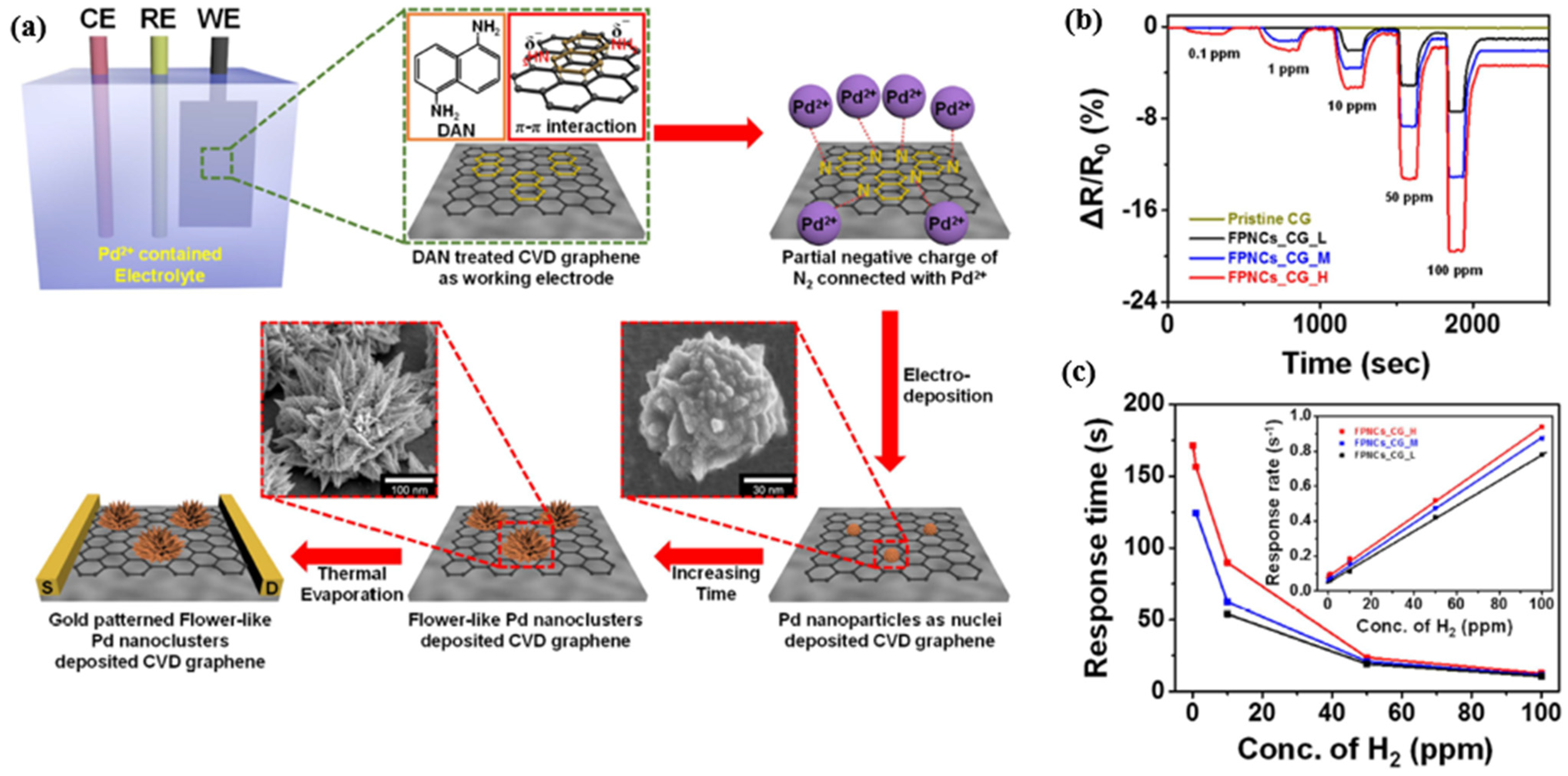
- Shin, D.H.; Lee, J.S.; Jun, J.; An, J.H.; Kim, S.G.; Cho, K.H.; Jang, J. Flower-like palladium nanoclusters decorated graphene electrodes for ultrasensitive and flexible hydrogen gas sensing. Sci. Rep. 2015, 5, 1–11. [Google Scholar] [CrossRef] [Green Version]
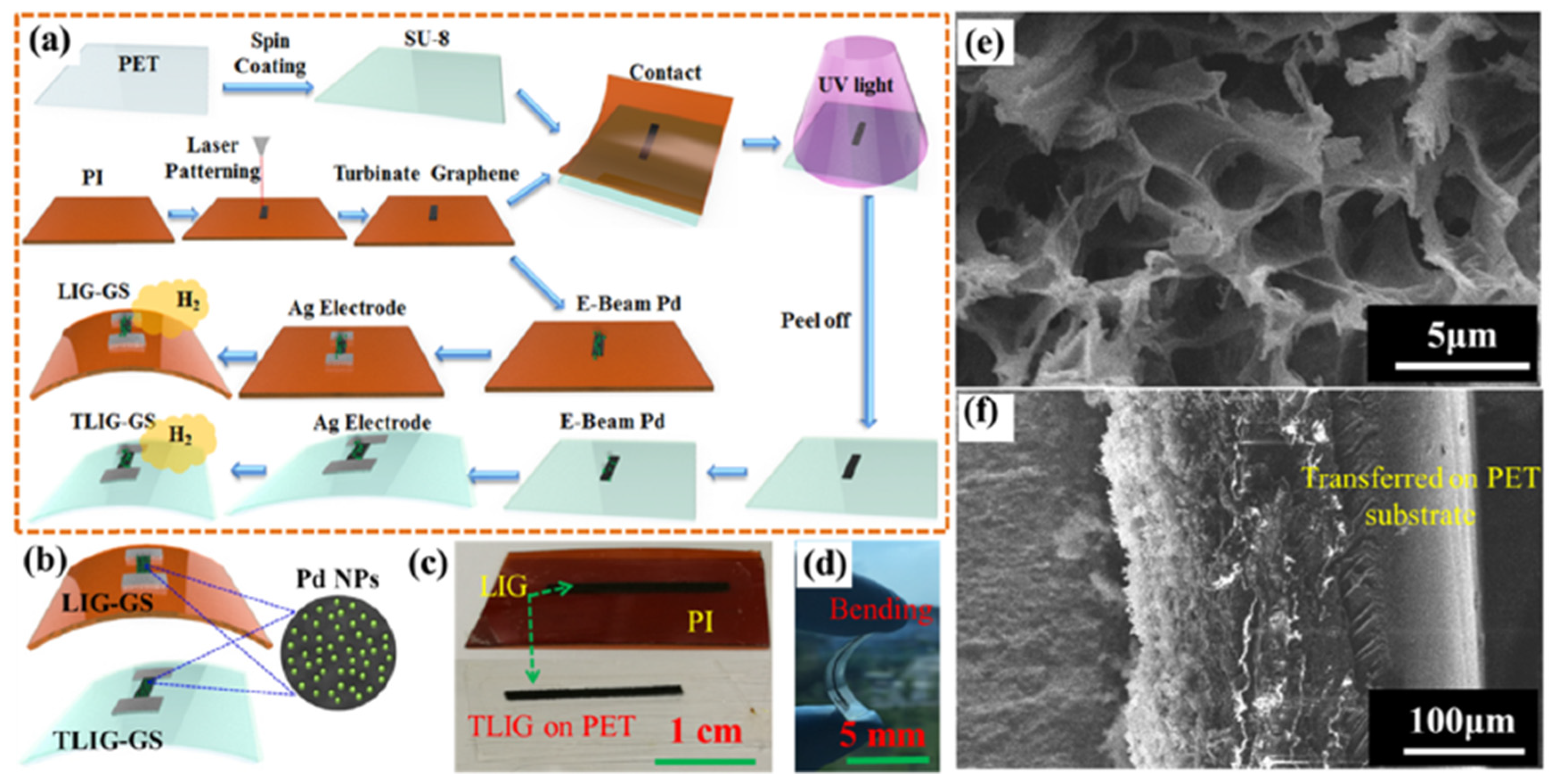
- Zhu, J.X.; Cho, M.; Li, Y.T.; Cho, I.; Suh, J.H.; Orbe, D.D.; Jeong, Y.; Ren, L.T.; Park, I. Biomimetic turbinate-like artificial nose for hydrogen detection based on 3D porous laser-induced graphene. ACS Appl. Mater. Interfaces 2019, 11, 24386–24394. [Google Scholar] [CrossRef] [PubMed]
- Li, D.S.; Le, X.H.; Pang, J.T.; Xie, J. A SAW hydrogen sensor based on the composite of graphene oxide and palladium nanoparticles. In Proceedings of the IEEE 32nd International Conference on Micro Electro Mechanical Systems (MEMS), Seoul, Korea, 27–31 January 2019; pp. 500–503. [Google Scholar]
- Phan, D.T.; Youn, J.S.; Jeon, K.J. High-sensitivity and fast-response hydrogen sensor for safety application using Pt nanoparticle-decorated 3D graphene. Renew. Energy 2019, 144, 167–171. [Google Scholar] [CrossRef]
- Zheng, Y.; Lee, D.; Koo, H.Y.; Maeng, S. Chemically modified graphene/PEDOT: PSS nanocomposite films for hydrogen gas sensing. Carbon 2015, 81, 54–62. [Google Scholar] [CrossRef]
- Harley-Trochimczyk, A.; Chang, J.Y.; Zhou, Q.; Dong, J.; Pham, T.; Worsley, M.A.; Maboudian, R.; Zettl, A.; Mickelson, W. Catalytic hydrogen sensing using microheated platinum nanoparticle-loaded graphene aerogel. Sens. Actuators B Chem. 2015, 206, 399–406. [Google Scholar] [CrossRef] [Green Version]
- Lu, X.J.; Song, X.J.; Gu, C.P.; Ren, H.B.; Sun, Y.F.; Huang, J.R. Freeze drying-assisted synthesis of Pt@ reduced graphene oxide nanocomposites as excellent hydrogen sensor. J. Phys. Chem. Solids 2018, 116, 324–330. [Google Scholar] [CrossRef]
- Lee, J.S.; Oh, J.; Jun, J.; Jang, J. Wireless hydrogen smart sensor based on Pt/graphene-immobilized radio-frequency identification tag. ACS Nano 2015, 9, 7783–7790. [Google Scholar] [CrossRef]
- Sharma, B.; Kim, J.S. Graphene decorated Pd-Ag nanoparticles for H2 sensing. Int. J. Hydrogen Energy 2018, 43, 11397–11402. [Google Scholar] [CrossRef]
- Anand, K.; Singh, O.; Singh, M.P.; Kaur, J.; Singh, R.C. Hydrogen sensor based on graphene/ZnO nanocomposite. Sens. Actuators B Chem. 2014, 195, 409–415. [Google Scholar] [CrossRef]
- Rasch, F.; Postica, V.; Schütt, F.; Mishra, Y.K.; Nia, A.S.; Lohe, M.R.; Feng, X.L.; Adelung, R.; Lupan, O. Highly selective and ultra-low power consumption metal oxide based hydrogen gas sensor employing graphene oxide as molecular sieve. Sens. Actuators B Chem. 2020, 320, 128363. [Google Scholar] [CrossRef]
- Das, S.; Roy, S.; Bhattacharya, T.S.; Sarkar, C.K. Efficient room temperature hydrogen gas sensor using ZnO nanoparticles-reduced graphene oxide nanohybrid. IEEE Sens. J. 2020, 21, 1264–1272. [Google Scholar] [CrossRef]
- Galstyan, V.; Comini, E.; Kholmanov, I.; Faglia, G.; Sberveglieri, G. Reduced graphene oxide/ZnO nanocomposite for application in chemical gas sensors. RSC Adv. 2016, 6, 34225–34232. [Google Scholar] [CrossRef]
- Pal, P.; Yadav, A.; Chauhan, P.S.; Parida, P.K.; Gupta, A. Reduced graphene oxide based hybrid functionalized films for hydrogen detection: Theoretical and experimental studies. Sens. Int. 2021, 2, 100072. [Google Scholar] [CrossRef]
- Drmosh, Q.A.; Yamani, Z.H.; Hendi, A.H.; Gondal, M.A.; Moqbel, R.A.; Saleh, T.A.; Khan, M.Y. A novel approach to fabricating a ternary rGO/ZnO/Pt system for high-performance hydrogen sensor at low operating temperatures. Appl. Surf. Sci. 2019, 464, 616–626. [Google Scholar] [CrossRef]
- Huang, J.R.; Wang, L.Y.; Shi, C.C.; Dai, Y.J.; Gu, C.P.; Liu, J.H. Selective detection of picric acid using functionalized reduced graphene oxide sensor device. Sens. Actuators B Chem. 2014, 196, 567–573. [Google Scholar] [CrossRef]
- Ren, H.B.; Gu, C.P.; Joo, S.W.; Cui, J.Y.; Sun, Y.F.; Huang, J.R. Preparation of SnO2 nanorods on reduced graphene oxide and sensing properties of as-grown nanocomposites towards hydrogen at low working temperature. Mater. Express 2018, 8, 263–271. [Google Scholar] [CrossRef]
- Kamal, T. High performance NiO decorated graphene as a potential H2 gas sensor. J. Alloy. Compd. 2017, 729, 1058–1063. [Google Scholar] [CrossRef]
- Dhall, S.; Kumar, M.; Bhatnagar, M.; Mehta, B.R. Dual gas sensing properties of graphene-Pd/SnO2 composites for H2 and ethanol: Role of nanoparticles-graphene interface. Int. J. Hydrogen Energy 2018, 43, 17921–17927. [Google Scholar] [CrossRef]
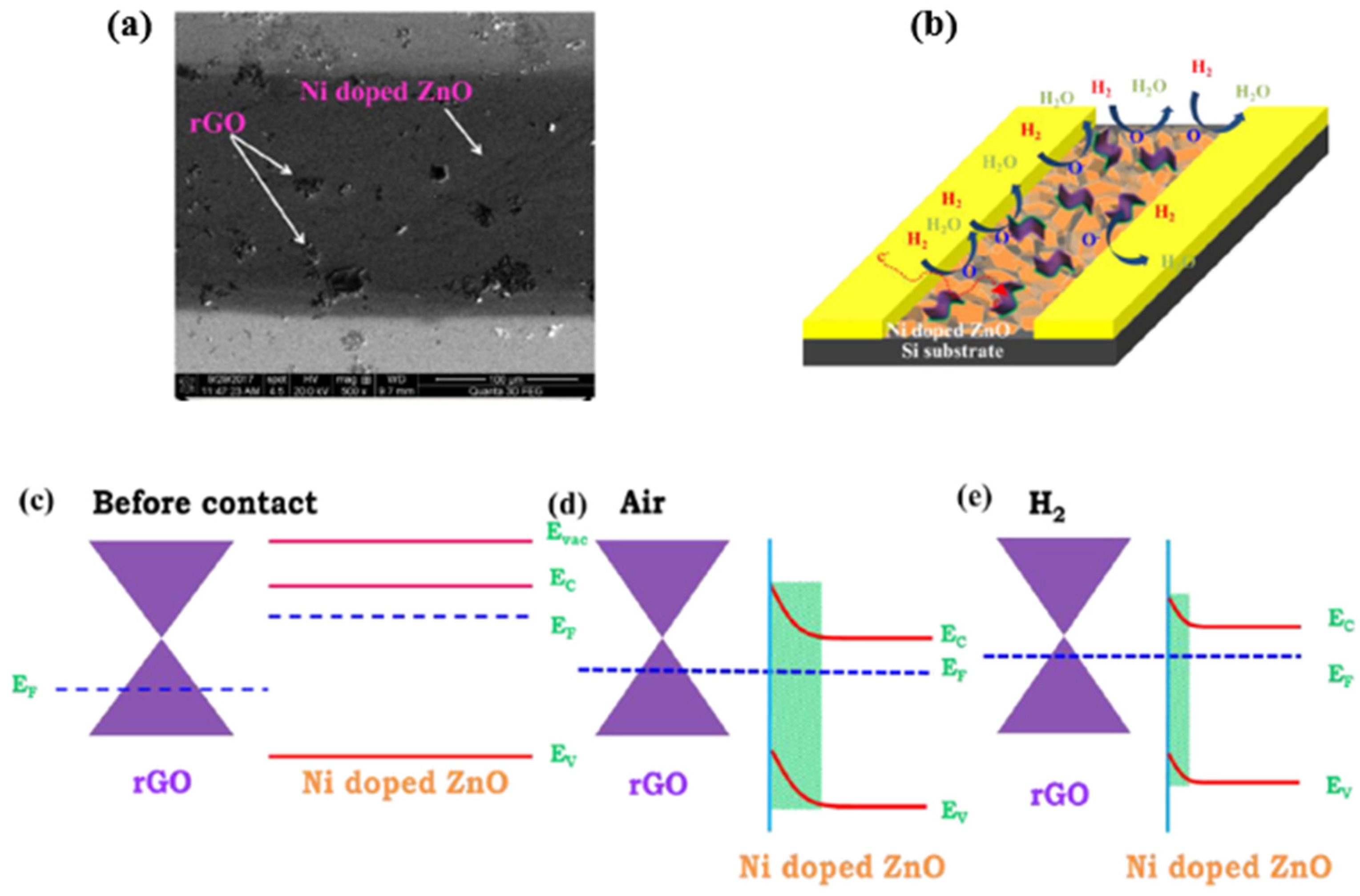
- Bhati, V.S.; Ranwa, S.; Rajamani, S.; Kumari, K.; Raliya, R.; Biswas, P.; Kumar, M. Improved sensitivity with low limit of detection of a hydrogen gas sensor based on rGO-loaded Ni-doped ZnO nanostructures. ACS Appl. Mater. Interfaces 2018, 10, 11116–11124. [Google Scholar] [CrossRef] [PubMed]
- Zhang, M.; Zhen, Y.H.; Sun, F.H.; Xu, C. Hydrothermally synthesized SnO2-graphene composites for H2 sensing at low operating temperature. Mater. Sci. Eng. B 2016, 209, 37–44. [Google Scholar] [CrossRef]
- Van Quang, V.; Van Dung, N.; Sy Trong, N.; Duc Hoa, N.; Van Duy, N.; Van Hieu, N. Outstanding gas-sensing performance of graphene/SnO2 nanowire Schottky junctions. Appl. Phys. Lett. 2014, 105, 013107. [Google Scholar] [CrossRef]
- Lee, J.H.; Katoch, A.; Choi, S.W.; Kim, J.H.; Kim, H.W.; Kim, S.S. Extraordinary improvement of gas-sensing performances in SnO2 nanofibers due to creation of local p–n heterojunctions by loading reduced graphene oxide nanosheets. ACS Appl. Mater. Interfaces 2015, 7, 3101–3109. [Google Scholar] [CrossRef]
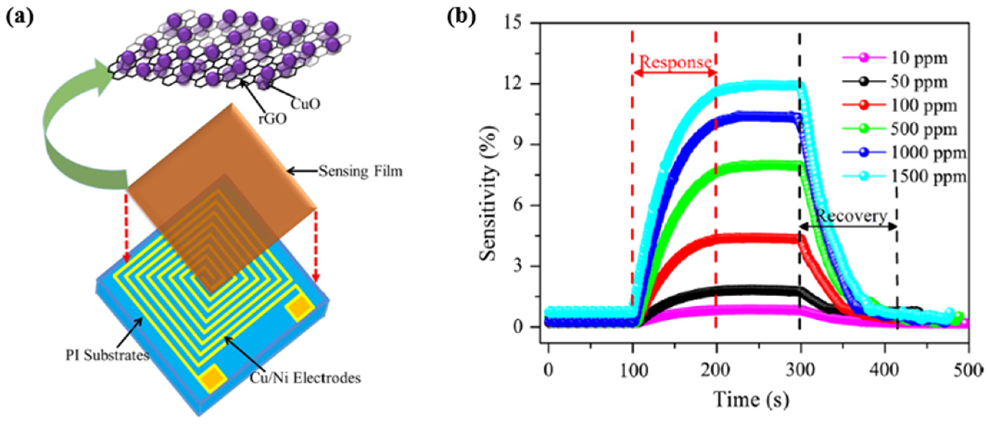
- Zhang, D.Z.; Yin, N.L.; Jiang, C.X.; Xia, B.K. Characterization of CuO–reduced graphene oxide sandwiched nanostructure and its hydrogen sensing characteristics. J. Mater. Sci. Mater. Electron. 2017, 28, 2763–2768. [Google Scholar] [CrossRef]
- Zhang, J.T.; Liu, J.F.; Peng, Q.; Wang, X.; Li, Y.D. Nearly monodisperse Cu2O and CuO nanospheres: Preparation and applications for sensitive gas sensors. Chem. Mater. 2006, 18, 867–871. [Google Scholar] [CrossRef]
- Dutta, D.; Hazra, S.K.; Das, J.; Sarkar, C.K.; Basu, S. Studies on p-TiO2/n-graphene heterojunction for hydrogen detection. Sens. Actuators B Chem. 2015, 212, 84–92. [Google Scholar] [CrossRef]
- Venkatesan, A.; Rathi, S.; Lee, I.Y.; Park, J.; Lim, D.; Kang, M.; Joh, H.I.; Kim, G.H.; Kannan, E.S. Molybdenum disulfide nanoparticles decorated reduced graphene oxide: Highly sensitive and selective hydrogen sensor. Nanotechnology 2017, 28, 365501. [Google Scholar] [CrossRef]
- Peng, Y.T.; Zheng, L.L.; Zou, K.; Li, C. Enhancing performances of a resistivity-type hydrogen sensor based on Pd/SnO2/RGO nanocomposites. Nanotechnology 2017, 28, 215501. [Google Scholar] [CrossRef] [PubMed]
- Venkatesan, A.; Rathi, S.; Lee, I.Y.; Park, J.; Lim, D.; Kim, G.H.; Kannan, E.S. Low temperature hydrogen sensing using reduced graphene oxide and tin oxide nanoflowers based hybrid structure. Semicond. Sci. Technol. 2016, 31, 125014. [Google Scholar] [CrossRef]
- Esfandiar, A.; Irajizad, A.; Akhavan, O.; Ghasemi, S.; Gholami, M.R. Pd–WO3/reduced graphene oxide hierarchical nanostructures as efficient hydrogen gas sensors. Int. J. Hydrogen Energy 2014, 39, 8169–8179. [Google Scholar] [CrossRef]
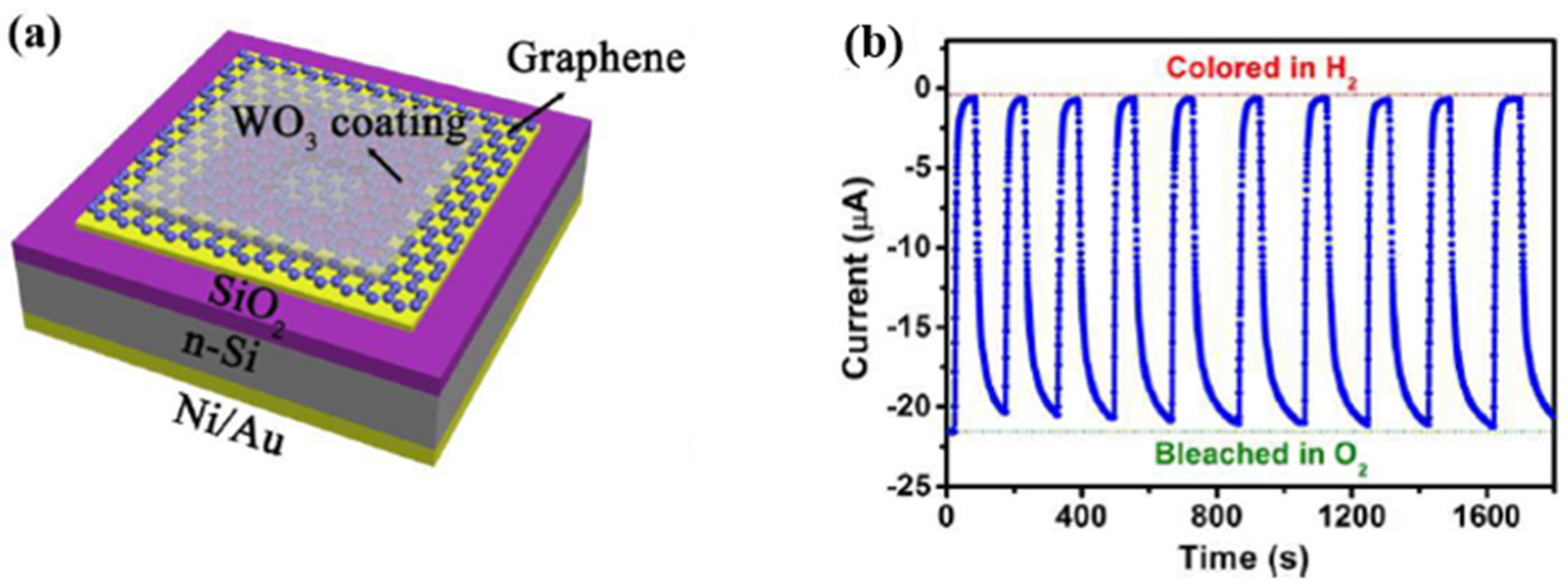
- Chen, M.Y.; Zou, L.P.; Zhang, Z.H.; Shen, J.; Li, D.; Zong, Q.J.; Gao, G.H.; Wu, G.M.; Shen, J.; Zhang, Z.X. Tandem gasochromic-Pd-WO3/graphene/Si device for room-temperature high-performance optoelectronic hydrogen sensors. Carbon 2018, 130, 281–287. [Google Scholar] [CrossRef]
- Bhati, V.S.; Ranwa, S.; Fanetti, M.; Valant, M.; Kumar, M. Efficient hydrogen sensor based on Ni-doped ZnO nanostructures by RF sputtering. Sens. Actuators B Chem. 2018, 255, 588–597. [Google Scholar] [CrossRef]
- Ayesh, A.I.; Alyafei, A.A.; Anjum, R.S.; Mohamed, R.M.; Abuharb, M.B.; Salah, B.; El-Muraikhi, M. Production of sensitive gas sensors using CuO/SnO2 nanoparticles. Appl. Phys. A 2019, 125, 1–8. [Google Scholar] [CrossRef] [Green Version]
- Li, X.M.; Zhu, H.W.; Wang, K.L.; Cao, A.Y.; Wei, J.Q.; Li, C.Y.; Li, Z.; Li, X.; Wu, D.H. Graphene-on-silicon Schottky junction solar cells. Adv. Mater. 2010, 22, 2743–2748. [Google Scholar] [CrossRef]
- Zhang, Q.C.; Wang, X.J.; Li, D.; Zhang, Z.X. Direct growth of nanographene on silicon with thin oxide layer for high-performance nanographene-oxide-silicon diodes. Adv. Funct. Mater. 2014, 24, 7613–7618. [Google Scholar] [CrossRef]
- Feng, W.; Wu, G.M.; Gao, G.H. Ordered mesoporous WO3 film with outstanding gasochromic properties. J. Mater. Chem. A 2014, 2, 585–590. [Google Scholar] [CrossRef]


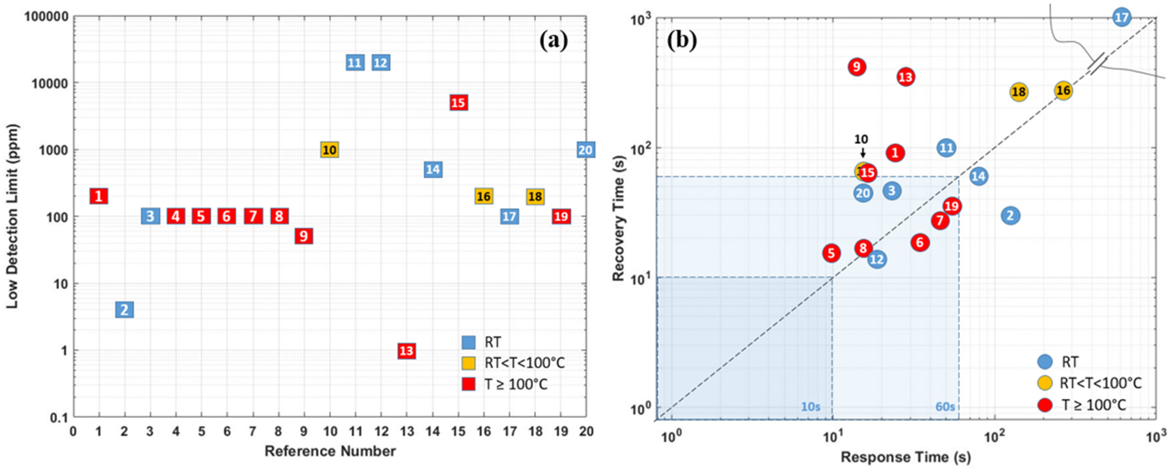
| Ref. Nr. | Sensor Materials | Operating Temperature | Synthesis Methods | Low Detection Limit | Literature | |
|---|---|---|---|---|---|---|
| 1 | Pd film | RT | DC sputtering | 100 ppm | 25/10 s (17%) at 1.2% | [58] |
| 2 | Pd film/Pt heater | 50 °C | --- | 200 ppm | 30/17 s (0.2%) at 4000 ppm | [59] |
| 3 | Pd film/Pt heater | 400 °C | --- | 200 ppm | 10/15 s (4%) at 4000 ppm | [59] |
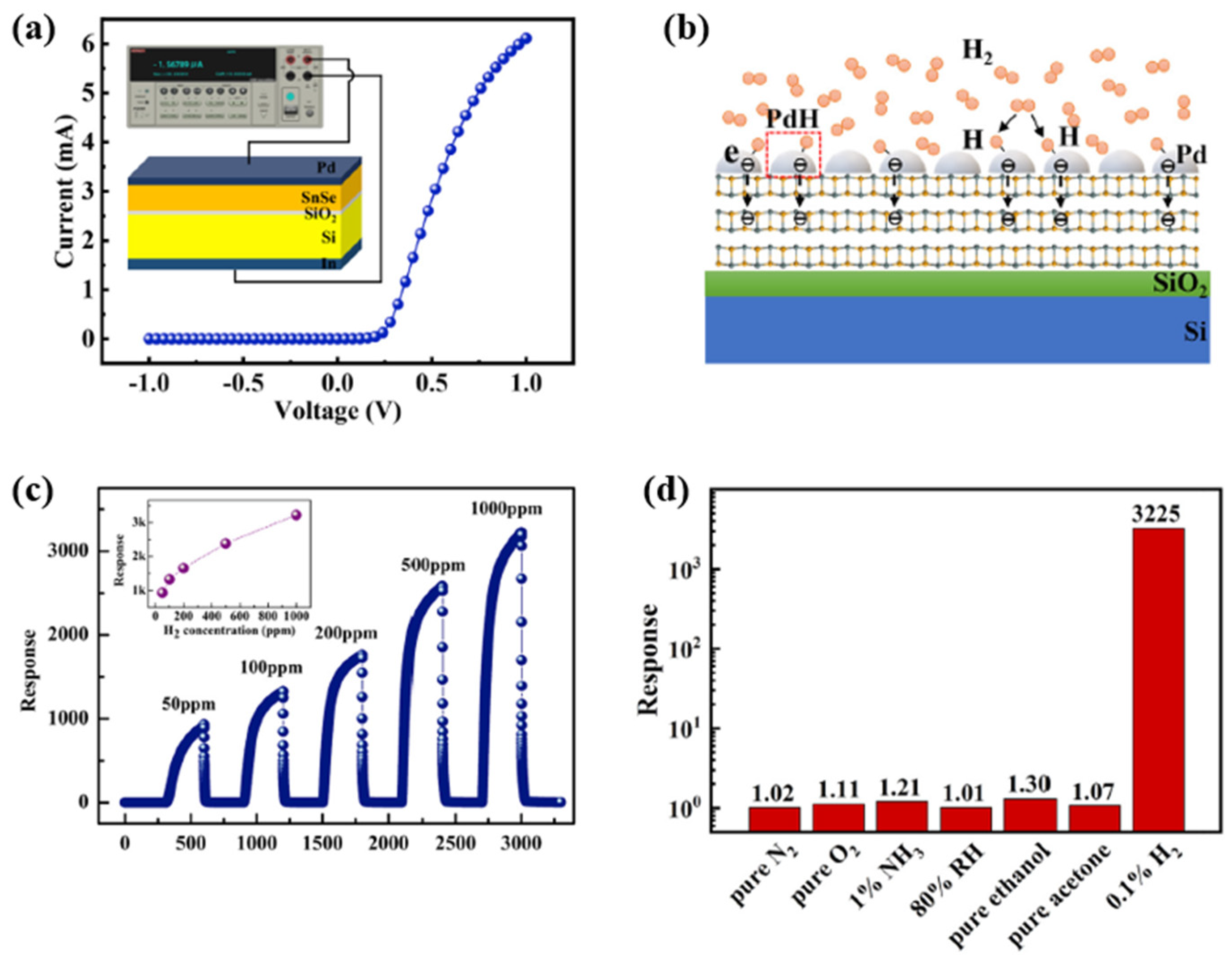
| 4 | Pd/SnSe film | RT | DC magnetron sputtering | 0.91 ppb | 73.1/23.7 s (3225 *) at 1000 ppm | [61] |
| 5 | film | RT | DC magnetron sputtering | 0.4% | 4/8 s (−) at 0.4% | [60] |
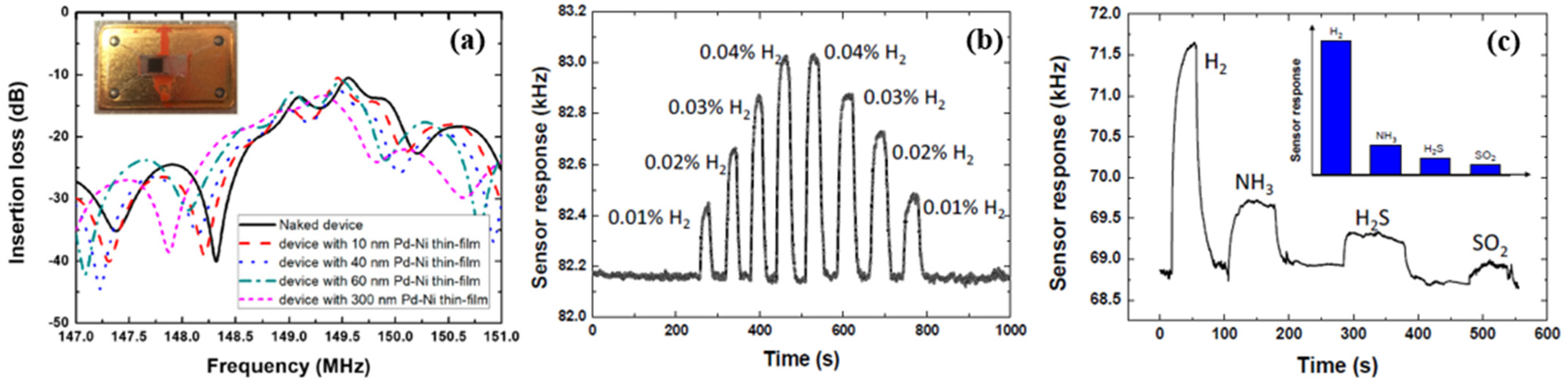
| 6 | Pd-Ni alloy thin-film | RT | RF magnetron co-sputtering, SAW | 0.01% | 7/30 s (2.75 kHz) at 0.1%, | [33] |
| 7 | Pd/ZnO film | RT | pulsed laser deposition | 0.2% | 12/16 s (−) at 2% | [39] |
| 8 | Pd/Y alloy film | RT | magnetron co-sputtering | 0.1% | 33/27 s (24.1 mV) at 1% | [32] |
| 9 | Pd/Co NWs | RT | electrodeposition | 0.1% | 200/500 s (~0.2%) at 1% | [64] |
| 10 | PA Pd NWs | RT | deposition | 0.1% | 70/140 s (~7%) at 1% | [66] |
| 11 | Pd-Si NWs | 200–400 °C | PVD | 0.01% | 10/30 s (1.5 *) at 0.1% | [69] |
| 12 | Pd NTs | 296–336 K | electrospun, deposition | 314 ppm | 12/18 s **(2.1%) at 1.8% | [72] |
| 13 | Pd/Cu NWs | RT | electrodeposition | 7 ppm | 4/4 s (1.5 kHz) at 1% | [73] |
| 14 | Pd/Si NWs | RT | DC magnetron sputtering | 5 ppm | −/− | [74] |
| 15 | Pd NWs @ZIF-8_2h | RT | lithographically patterned nanowire, electrodeposition | 1000 ppm | 13/6 s (0.3%) at 0.1% | [75] |
| 16 | Pd NWs @ZIF-8_4h | RT | lithographically patterned nanowire, electrodeposition | 600 ppm | 30/8 s (0.7%) at 0.1% | [75] |
| 17 | 160 °C | electrospun, magnet sputtering | 0.25 ppm | 4 s/− (30 *) at 100 ppm | [77] | |
| 18 | /Si | RT | Deposition | 2% | 6/45 s (51.4%) at 2% | [78] |
| 19 | /Si | RT | Deposition | 1% | 1.4 s/14 s (88%) at 1% | [79] |
| 20 | /Si | RT | deposition, Spin coating | 100 ppm | −/− | [82] |
| 21 | Pd NPs / ZnO | RT | RF magnetron sputtering | 0.5 ppm | 18.8 s/− (91.2%) at 0.1% | [86] |
| 22 | 200 °C | solvothermal method | 10 ppm | 4/10 s (315.34 *) at 3000 ppm | [87] | |
| 23 | NWs | 300 °C | chemical Deposition | 1 ppm | 150/400 s ** (27.8 *) at 100 ppm | [88] |
| 24 | Pd/BN/ZnO NWs | 200 °C | atomic layer deposition | 0.5 ppm | 160/90 s (7.95 *) at 10 ppm | [93] |
| Ref. Nr. | Sensor Materials | Operating Temperature | Synthesis Methods | Low Detection Limit | Literature | |
|---|---|---|---|---|---|---|
| 1 | NW | 150 °C | DC sputtering | 10 ppm | −/− () at 1000 ppm | [105] |
| 2 | NPs | 350 °C | thermal evaporation method | 400 ppm | 11/17 s ** (4.5 V) at 400 ppm | [106] |
| 3 | NFs | RT | hydrothermal method | 100 ppm | 63/500 s (80.20%) at 1000 ppm | [111] |
| 4 | 200 °C | solvothermal method | 10 ppm | 4/10 s (315.34 *) at 3000 ppm | [87] | |
| 5 | Film | 175 °C | magnetron sputtering method | 100 ppm | 1/512 s (115.9 kHz) at 2000 ppm | [112] |
| 6 | RT | hydrothermal method, irradiated photochemical reduction method | 100 ppm | 0.33/29.60 s (88.35%) at 1000 ppm | [113] | |
| 7 | 350 °C | sol-gel and hydrothermal methods | 0.08 ppm | 29/36 s (~60 *) at 100 ppm | [114] | |
| 8 | 200 °C | hydrothermal method | 1 ppb | 1/3 s (25 *) at 100 ppm | [115] | |
| 9 | Pd/ZnO NFs | 250 °C | hydrothermal method, UV reduction method | 0.5 ppm | 450/500 s (2.5 *) at 50 ppm | [122] |
| 10 | ZnO | 400 °C | Wet chemical method | 2000 ppm | 5/7 s (10 *) at 2000 ppm | [107] |
| 11 | ZnO rods | 350 °C | --- | 10 ppm | 700/1100 s ** (−) at 100 ppm | [121] |
| 12 | Hollow ZnO particles | 225 °C | hydrothermal | 2 ppm | 139 s/>30 min ** (89%) at 100 ppm | [125] |
| 13 | ZnO NFs | 350 °C | electrospinning | 0.1 ppm | 400/200 s ** (74.7 *) at 100 ppb | [126] |
| 14 | NFs | 330 °C | electrospinning | 25 ppm | 69/175 s (10 *) at 100 ppm | [123] |
| 15 | NFs | 300 °C | electrospinning, Ar plasma | 10 ppm | 24/165 s (18 *) at 100 ppm | [123] |
| 16 | NFs | 300 °C | electrospinning | 50 ppb | −/− (50.1 *) at 50 ppb | [127] |
| 17 | TiO | RT | reactive DC magnetron sputtering | 30 ppm | *) at 1000 ppm | [128] |
| 18 | Pt/TiO | RT | pressing, sintering | 30 ppm | 10/20 s (6000 *) at 1000 ppm | [129] |
| 19 | RT | electrostatic spray deposition (ESD) | 0.2% | 15 s/10 min (18.5 *) at 1% | [131] | |
| 20 | RT | fermto second laser, hydrothermal method | 0.02% | 15/33 s (522 pm%(v/v)) at 1% | [136] | |
| 21 | /ZnO | 350 °C | electrospinning, ultraviolet irradiation method | 50 ppb | −/− (172 *) at 50 ppb | [141] |
| Ref. Nr. | Sensor Material | Operating Temperatur | Method | Low Detection Limit | Liter-ature | |
|---|---|---|---|---|---|---|
| 1 | G | RT | CVD, e-beam evaporation | 200 ppm | 1/3 min (−) at 0.1% | [157] |
| 2 | GO | RT | Modified Hummer method and spray pyrolysis method | 60 sccm | 100/437.2 s (16.16%) | [159] |
| 3 | rGO | RT | Modified Hummers method | 200 ppm | 11/36 s (6%) at 200 ppm | [160] |
| 4 | Pd/G | RT | CVD | 1% | 3/9 min (5.88%) at 1% | [162] |
| 5 | Pd/rGO | RT | HTRJ process | 25 ppm | 73/126 s (14.8%) at 2% | [170] |
| 6 | Pd/G | RT | CVD, dip-coating process | 200 ppm | 18/300 s (−) at 0.5% | [163] |
| 7 | Pd/G | 180 °C | Exfoliation, Soft lithography | 10 ppm | 15/16 s (−) at 100 ppm | [164] |
| 8 | Pd/G | 254 °C | Deposition | 1 ppm | 16/14 s (−) at 1000 ppm | [165] |
| 9 | PMMA/Pd/G | RT | CVD | 250 ppm | 1.81/5.52 min (66.7%) at 2% | [85] |
| 10 | Pd/GO | RT | CVD | 0.5% | 6/7 s (−) at 1% | [181] |
| 11 | Pt/G | 200 °C | Polymer-assisted hydrothermal (HT) method | 10 ppm | 9/10 s (−) at 1% | [182] |
| 12 | PEDOT:PSS/GO | RT | Modified Hummers’ method | 30 ppm | 30/25 s (4.2%) at 100 ppm | [183] |
| 13 | Pd/PANI/rGO | RT | Chemical reduction | 100 ppm | 20/50 s (25%) at 1% | [176] |
| 14 | Pt/G | RT | Hummers’ method | 500 ppm | 0.97/0.92 s (1.6%) at 1% | [184] |
| 15 | Pt/rGO | 50 °C | Modified Hummers’ method | 0.3% | 63/104 s (−) at 0.5% | [185] |
| 16 | Pt/rGO | RT | Modified Hummers and Offman method | 1 ppm | −/− | [186] |
| 17 | Pd/Ag/G | 70–190 °C | Spin Coating, Sputter | 100 ppm | 56 s/− (15.23%) at 500 ppm | [187] |
| 18 | Pd/G | RT | CVD | 0.1 ppm | 12/15 s (−) at 100 ppm | [179] |
| 19 | Pd/LIG | RT | Laser-induced graphene (LIG) | 600 ppm | 6/20 min (−) at 1% | [180] |
| Ref. Nr. | Sensor Material | Operating Temperature | Method | Low Detection Limit | Literature | |
|---|---|---|---|---|---|---|
| 1 | ZnO/G | 150 °C | Hummer’s method | 200 ppm | 22/90 s (3.5 *) at 200 ppm | [188] |
| 2 | ZnO/GO | RT | simple wet-chemical coating technique | 4 ppm | 114/30 s (3.42 *) at 1000 ppm | [189] |
| 3 | ZnO/rGO | RT | Electrochemical exfoliation | 100 ppm | 21.04/47.09 s (484.1% *) at 100 ppm | [190] |
| 4 | ZnO/rGO | 250 °C | Modified Hummers method [C23] | 100 ppm | −/− (30%) at 500 ppm | [191] |
| 5 | ZnO/Ag/Pd/rGO | 150 °C | Modified Hummers method | 100 ppm | 10/14 s (59%) at 100 ppm | [192] |
| 6 | ZnO/rGO | 150 °C | Modified Hummers method | 100 ppm | 33/19 s (46%) at 100 ppm | [192] |
| 7 | Ag/ZnO/rGO | 150 °C | Modified Hummers method | 100 ppm | 45/27 s (51%) at 100 ppm | [192] |
| 8 | ZrO2/ZnO/rGO | 150 °C | Modified Hummers method | 100 ppm | 15/16 s (52%) at 100 ppm | [192] |
| 9 | Pt/ZnO/rGO | 100 °C | Modified Hummers method | 50 ppm | 12/412 s (99%) at 400 ppm | [193] |
| 10 | SnO2/rGO | 80 °C | Modified Hummers method | 1000 ppm | 15/61 s(1.58%) at 1000 ppm | [195] |
| 11 | Pd/SnO2/G | RT | CVD | 2% | 50/100 s (11%) at 2% | [197] |
| 12 | SnO2/G | RT | CVD | 2% | 18/12 s (0.35%) at 2% | [197] |
| 13 | Ni/ZnO/rGO | 150 °C | Hummer‘s method | 1 ppm | 28/320 s (63.8%) at 100 ppm | [198] |
| 14 | CuO/rGO | RT | Thermal heating from GO at 180 °C | 50 ppm | 80/60 s (12%) at 1500 ppm | [202] |
| 15 | TiO2/G | 125 °C | Hummers’ chemical method | 5000 ppm | 16/61 s (18%) at 5000 ppm | [204] |
| 16 | MoS2/rGO | 60 °C | Modified Hummers method | 200 ppm | 261/260 s (15.6%) at 200 ppm | [205] |
| 17 | Pd/SnO2/rGO | RT | Modified Hummers method | 100 ppm | 600 s/>2000 s ** (55%) at 10,000 ppm | [206] |
| 18 | SnO2/rGO | 60 °C | Modified Hummers method | 200 ppm | 119.6 s/265 s (19.6%) at 1000 ppm | [207] |
| 19 | Pd/WO3/rGO | 100 °C | Modified Hummers method | 100 ppm | 52/35 s (150 *) at 500 ppm | [208] |
| 20 | Pd/WO3/G | RT | CVD-Method | 0.1% | 13/43 s(90%) at 4% | [208] |
Publisher’s Note: MDPI stays neutral with regard to jurisdictional claims in published maps and institutional affiliations. |
© 2021 by the authors. Licensee MDPI, Basel, Switzerland. This article is an open access article distributed under the terms and conditions of the Creative Commons Attribution (CC BY) license (https://creativecommons.org/licenses/by/4.0/).
Share and Cite
Wang, B.; Sun, L.; Schneider-Ramelow, M.; Lang, K.-D.; Ngo, H.-D. Recent Advances and Challenges of Nanomaterials-Based Hydrogen Sensors. Micromachines 2021, 12, 1429. https://doi.org/10.3390/mi12111429
Wang B, Sun L, Schneider-Ramelow M, Lang K-D, Ngo H-D. Recent Advances and Challenges of Nanomaterials-Based Hydrogen Sensors. Micromachines. 2021; 12(11):1429. https://doi.org/10.3390/mi12111429
Chicago/Turabian StyleWang, Bei, Ling Sun, Martin Schneider-Ramelow, Klaus-Dieter Lang, and Ha-Duong Ngo. 2021. "Recent Advances and Challenges of Nanomaterials-Based Hydrogen Sensors" Micromachines 12, no. 11: 1429. https://doi.org/10.3390/mi12111429
APA StyleWang, B., Sun, L., Schneider-Ramelow, M., Lang, K.-D., & Ngo, H.-D. (2021). Recent Advances and Challenges of Nanomaterials-Based Hydrogen Sensors. Micromachines, 12(11), 1429. https://doi.org/10.3390/mi12111429