1. Introduction
Nowadays, the even increase in energy consumption and the worldwide concern about environmental issues have led to increase the power generation through renewable sources, like photovoltaic and fuel-cell sources [
1,
2]. The output voltage of these alternative sources is low and unregulated [
3,
4]; therefore, an interface with DC-DC power converters is needed to obtain a high and regulated output voltage. [
5]. On the other hand, these energy sources can suffer permanent damage if high ripples appear in the demanded current [
6,
7]. According to the above, DC-DC switching power converters for renewable applications should have high-voltage gains, low-input current ripples and high-power efficiencies [
8].
The conventional boost converter has been proposed for renewable applications [
9,
10]; however, larger duty cycles are required to achieve high voltage gains. The above produces large voltage spikes, diode reverse recovery time problems, and high conduction losses on the active switch due to the intrinsic resistances [
11,
12].
In the open literature, several configurations are available to further extend the voltage gain without large duty cycles. A boost converter with a quadratic conversion ratio is discussed in [
13]. This configuration is based on stackable switching cells with a modular structure that can be extended to boost the output voltage. This converter exhibits a pulsating input current; therefore, a coupled capacitor is needed for renewable energy applications [
14]. A quadratic boost converter with two conventional boost converters connected in series (QBC-SC) is proposed in [
15]. The power flows in cascade from the input source to the first converter; then, the power flows to the second converter and later to the load.
The quadratic relationship of the conversion ratio provides a high-voltage gain for this configuration. A quadratic boost converter with a single switch (QBC-SS) is disscused in [
16]. It is similar to the QBC-SC, the power flows in series through the two converters and load; however, it includes only one switch. A QBC-SS that includes a voltage doubler to achieve an extra voltage gain (QBC-TR) is proposed in [
17]. It includes a voltage doubler to achieve an extra voltage gain. The voltage doubler consists of two capacitors, two diodes, and a coupled inductor that provides an additional gain respect to the quadratic conversion ratio. A current-fed boost converter with a quadratic voltage gain (QBC-CF) is proposed in [
18]. This converter has two operation modes. Energy from the input source is stored in two inductors; after that, the energy is transfer to two output capacitors. The quadratic gain is obtained by a series arrangement of capacitors, where the output voltage is the sum of both capacitor voltages. The number of diodes and the way to charge both inductors have an impact on the power efficiency. A boost converter with an active switched inductor-capacitor (LC) network is proposed in [
19]. The configuration consists of two inductors that are charged in parallel across two active switches, one diode, and one capacitor. This configuration uses a non-common grounding. The energy stored in both inductors is transferred in series to the output capacitor and the load. The structure of this configuration allows an enlargement of the conversion ratio respect to the gain of the quadratic boost converter. On the other hand, a coupling capacitor needs to be connected to the input of the converter because the input current has a pulsating waveform. Two boost configurations based on the quadratic and Cuk converters are shown in [
20]. These configurations offer an extra voltage gain by adding a factor increment to the quadratic voltage gain. They are classified into two types, depending on the voltage gain of each configuration. Both converters have non-common grounding. An isolated boost converter that includes forward and flyback configurations is proposed in [
21]. This converter is based on a quadratic configuration with an extended voltage gain because of the turns ratio of the transformer; however, the input current has a pulsating waveform.
The quadratic boost converter is a feasible option for processing energy generated by renewable sources, because it has a higher voltage conversion ratio. Quadratic conversion ratios can achieve higher voltage gains with duty cycles less than 0.7. This configuration generates a non-pulsating input current, which is critical for renewable sources as fuel and photovoltaic cells. The circuit of the conventional quadratic boost converter (QBC-SC) is depicted in
Figure 1.
A major drawback of the conventional quadratic configuration is the series power transfer between the input source and the load, resulting in a low overall efficiency. The above implies a reprocessing of the energy generated by the source; thus, a slow energy propagation between the input of the converter and the load is obtained. On the other hand, energy reprocessing yields an increment on the power losses due to the parasitics of the converter elements. This issue is described in
Figure 2, where the power is transferred throughout the two boost converters of the QBC-SC. As can be seen, the power flow is done in series between the input source and the load, where the capacitor
acts as the input source of the second converter.
A boost converter with a quadratic voltage gain, common ground, and non-series power transfer for better efficiency is proposed in this work. This configuration consists of two conventional boost converters with a transfer capacitor between both converters. This capacitor allows a parallel energy transfer between both converters and the output. The main advantage is an increase in power efficiency due to the non-series power transfer. Moreover, this configuration can be used for processing energy from alternative sources without the need to add a filter for reducing the input current ripple.
The organization of this work is as follows. A description and operation of the proposed configuration are shown in
Section 2. The state-steady conditions and the converter design are developed in
Section 3. The power efficiency of the proposed configuration is analyzed in
Section 4. Bilinear and linear models of the proposed converter are developed in
Section 5. Design criteria of the proposed converter are shown in
Section 6. Experimental verification with a 500 W laboratory prototype is provided in
Section 7. Final remarks are given in
Section 8.
2. Converter Operation
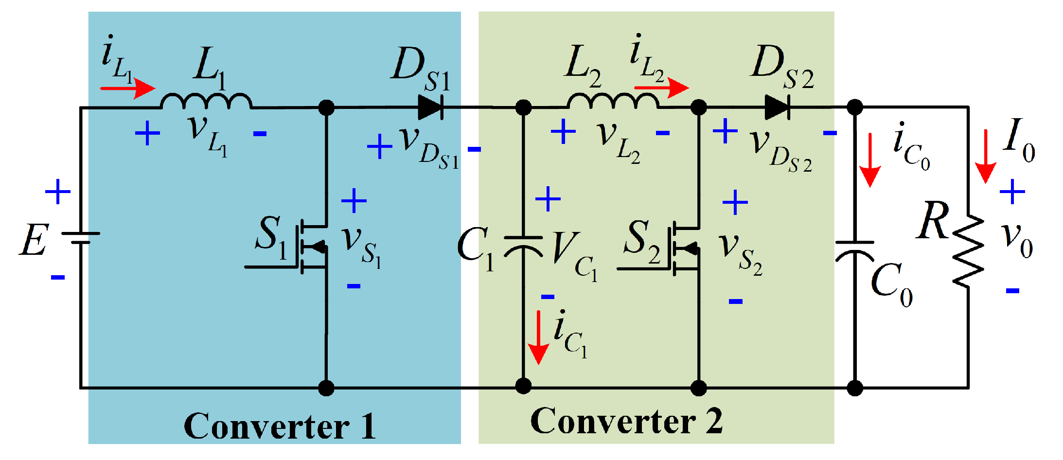
The proposed configuration is depicted in
Figure 3. The input voltage is represented by
E, the currents and voltages through
and
are denoted by
,
,
, and
, respectively. The voltages and currents through
, and
are denoted by
,
,
, and
, respectively. On the other hand, the voltages through
,
,
and
are denoted by
,
,
, and
. Finally, the current through the load
R is denoted by
.
The analysis is carried out considering the following points:
The study is developed for continuous conduction mode operation (CCM).
The passive elements (, , , ), the active switches (, ), and the passive switches (, ) are considered as an ideal components.
The active switches operate under the same duty cycle D. Thus, , is the switching frequency, and is the period of the PWM signal that drives the active switches.
For steady-state operation, , where and .
Due to the above assumptions, the proposed configuration operates in two modes. The power transfer from the input to the output of the proposed configuration is shown in
Figure 4. As can be seen, a non-series power transfer between the input source and the load occurs due to the transfer capacitor
.
The two operating modes of the converter are described as follows:
Mode I [
]: Both active switches (
,
) are turned ON. The diodes
and
are not conducting; then, the input source
E delivers energy to the inductor
. The inductor
is charged through capacitor
by the energy stored in the capacitor
, which also supplies energy to the load. The circuit that describes this operating mode is exhibited in
Figure 5.
Mode II [
]: Both active switches (
,
) are turned OFF. For this interval, the output capacitor
and the load
R are supplied by the energy stored in inductor
, through capacitor
. The inductor
delivers energy to the output (
and
R) through the diode
. The circuit that describes this operating mode is exhibited in
Figure 6.
The analysis, modeling, and the expressions in steady-state are easy to develop in two operating modes. On the other hand, the capacitor acts as a power transfer element between the first converter and the output capacitor . Due to this arrangement, the cascade power transfer between the first and second converter is avoided; thus, there is an improvement in the converter efficiency.
4. Study of the Power Efficiency
Now, the analysis and expressions for computing the power losses of each element for the proposed converter are provided. According to [
23], the corresponding circuit including the parasitics of all elements of the configuration is exhibited in
Figure 8. The resistances
,
,
,
,
,
,
, and
are the equivalent series resistance (ESR) of
,
,
,
,
,
,
, and
, respectively. The voltages
and
are the forward voltage drops of
, and
. The gate voltage for
and
is
. In the interval
, both active switches are conducting. The respective circuit for this interval is described in
Figure 9. On the other hand, the respective circuit for the interval
(both active switches are not conducting) is depicted in
Figure 10.
Using the volt-second balance principle over
and
, two expressions for
are derived. From these two expressions, it is possible to find the relationship for computing the duty cycle (
) and the losses of each component of the converter. To precisely quantify the losses associated with the parasitics of the converter, it is necessary to recalculate the duty cycle (
). The resulting equation for
has a fourth-order behavior:
where:
to obtain the duty cycle
, it is necessary to solve Equation (
14) and choose the adequate root.
The expressions for the power losses of each element are shown in
Table 2 (conduction and switching losses are included). The diode junction capacitances of
and
are
and
, respectively. The time intervals are
,
,
, and
, where
,
,
,
,
,
,
, and
are the rise time, turn ON delay time, fall time, and turn OFF delay time of
, and
, respectively. The input capacitances of
and
are
and
, respectively. The RMS current values can be obtained as:
The expression for computing the power efficiency is:
where
is defined as
.
6. Converter Design
Now, the design of a 500 W power converter using the procedure shown in
Section 3 is now described. The input voltage
E is 30 V, the output voltage
is set to 220 V, and the load
R is
. A switching frequency of
kHz is selected with an ideal duty cycle of
. The selection criterion of the switching frequency was made based on the sizing of the passive elements, which increase in value with low switching frequencies. Due to the above, the power efficiency decreases when high inductance and capacitance values are selected. On the other hand, generally the value of the switching frequency used for medium and high power DC-DC converters ranges from 25 kHz to 100 kHz. The corresponding parameters for the designed converter are shown in
Table 3.
The theoretical power efficiency at the nominal load of the proposed configuration is 95.4%, which was obtained using (
14)–(
16). The parameters of
Table 2 were computed using the datasheet of the semiconductor devices used used to build the prototypes. The ESR values of the two inductors and two capacitors were measured using the meter model LCR-821 from GW Insteak. The theoretical duty cycle, including the power losses, is
.
Figure 11 shows a comparison between the ideal gain obtained with expression (
3) and the gain given in expression (
14), where all losses are included. It can be observed that both plots are similar until the duty cycle reaches 0.8; after that, the non-idealities produce a difference as shown in the plot.
7. Experimental Verification
Experimental verification with a 500 W laboratory prototype is provided in this section. The prototype was designed according to the parameters given in
Table 3, and it is shown in
Figure 12. The prototype for QBC-SC and QBC-SS converter is shown in
Figure 13. Both converters were built in the same prototype, only one switch was replaced by a diode and vice versa.
The experimental set-up of the converter is described in
Figure 14. The relationship of the voltage gain (
/
E) is 220 V/30 V, and the peak value of the ramp signal is 5 V. Additionally, QBC-SC (
Figure 15) and QBC-SS (
Figure 16) prototypes were built to compare the experimental power efficiencies of the three configurations.
For a fair comparison, all converters were built using the same components. For the QBC-SS, the active switch was replaced by the Schottky diode DSA90C200HB.
The parameters of the QBC-SC and the QBC-SS are shown in
Table 4. The parameters were obtained by using the expressions developed in [
26]. The theoretical and experimental plots for the comparison of efficiencies are shown in
Figure 17. The teoretical plot was obtained using the Equations (
14)–(
16), while the experimental plots of the three converter were obtained for a voltage gain of 220 V/30 V, and varying the load from
(100 W) to
(500 W), with steps of 100 W. The voltage and current values were obtained using the osciloscopie model MDO3034 and the current probe model TCP303 from Tektronix. As can be seen, the theoretical and experimental plots for the proposed converter are similar, only with small variations. The experimental efficiency of the proposed converter ranges from 97.8% (20% of nominal load) to 95.1% (nominal load). It can be noticed that the proposed configuration offers an improvement in the power efficiency due to the non-series power transfer. One part of the energy processed by the first converter flows directly to the output through the transfer capacitor without being reprocessed by the second converter. A pie chart of breakdown losses for nominal load is shown in
Figure 18. It is clear that the biggest losses are in the diodes and inductors, while the switch losses are not significant due to the low ESR value of both switches.
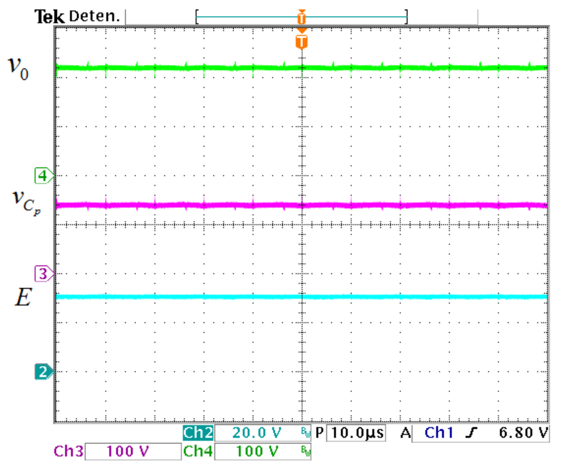
The inductor and output currents of the prototype are exhibited in
Figure 19. The average value of
is 17.5 A, the average value of
is 6.3 A, and for
is 2.7 A. In
Figure 20, the input and capacitors voltages are exhibited The value of
E is 30 V, the average transfer capacitor voltage
is 139 V, while the average output capacitor voltage
is 220 V.
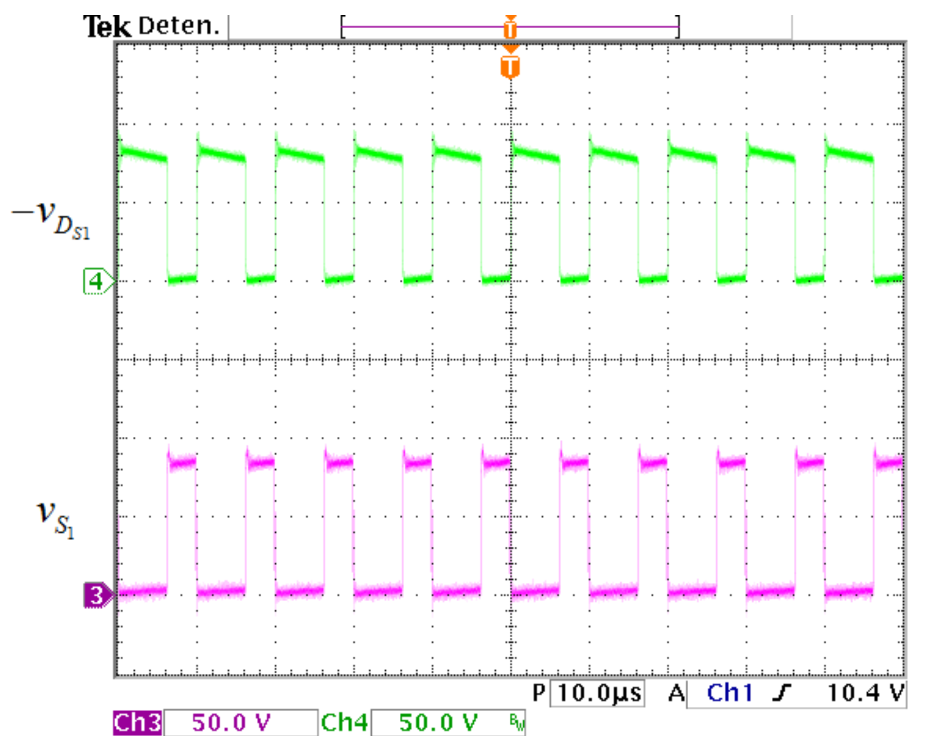
The voltage waveforms in the active switch
and the diode
are exhibited in
Figure 21. The voltage stress on
and
is 98 V. The voltage waveforms in the active switch
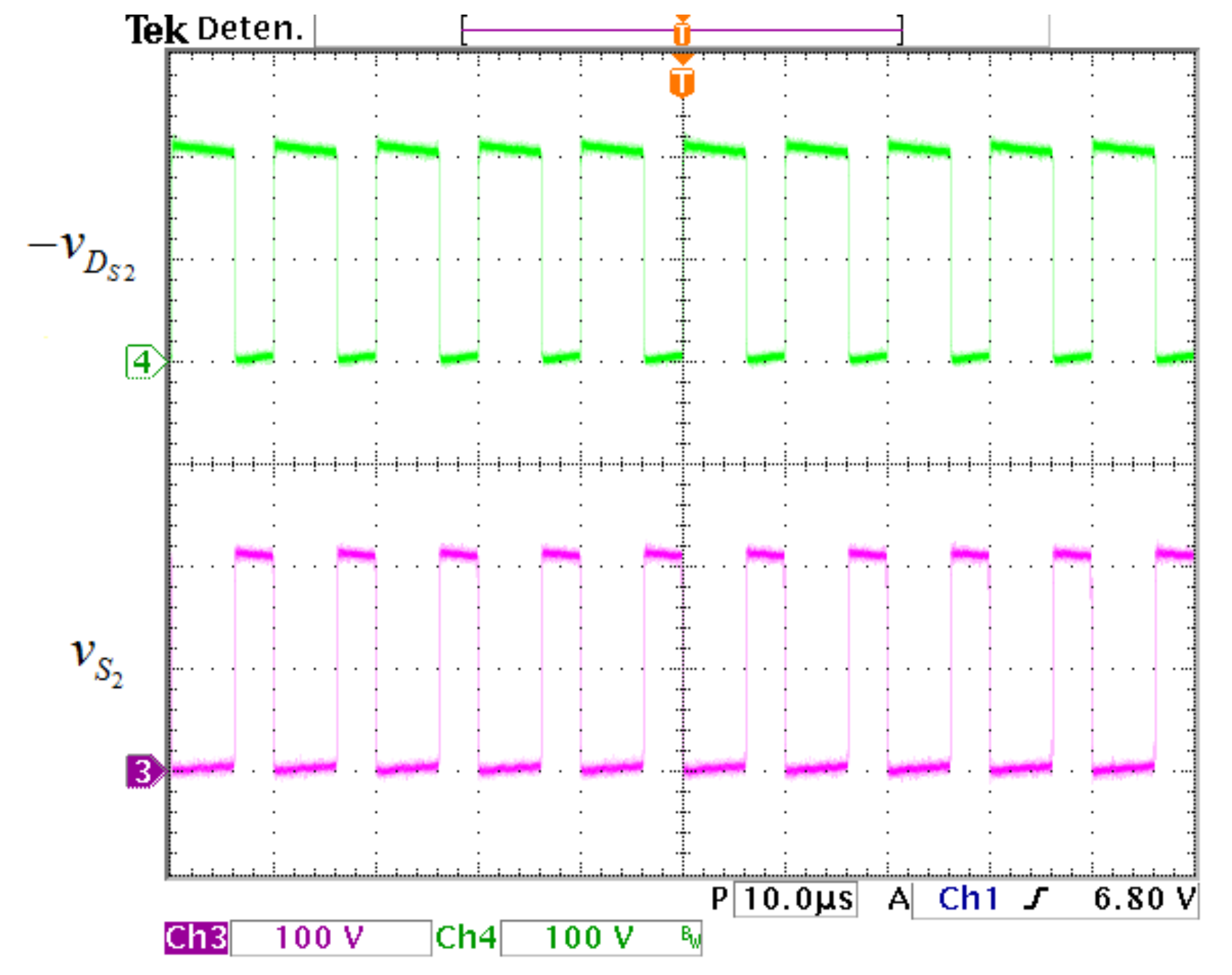
and the diode
are exhibited in
Figure 22, where the voltage stress on
and
is 222 V.
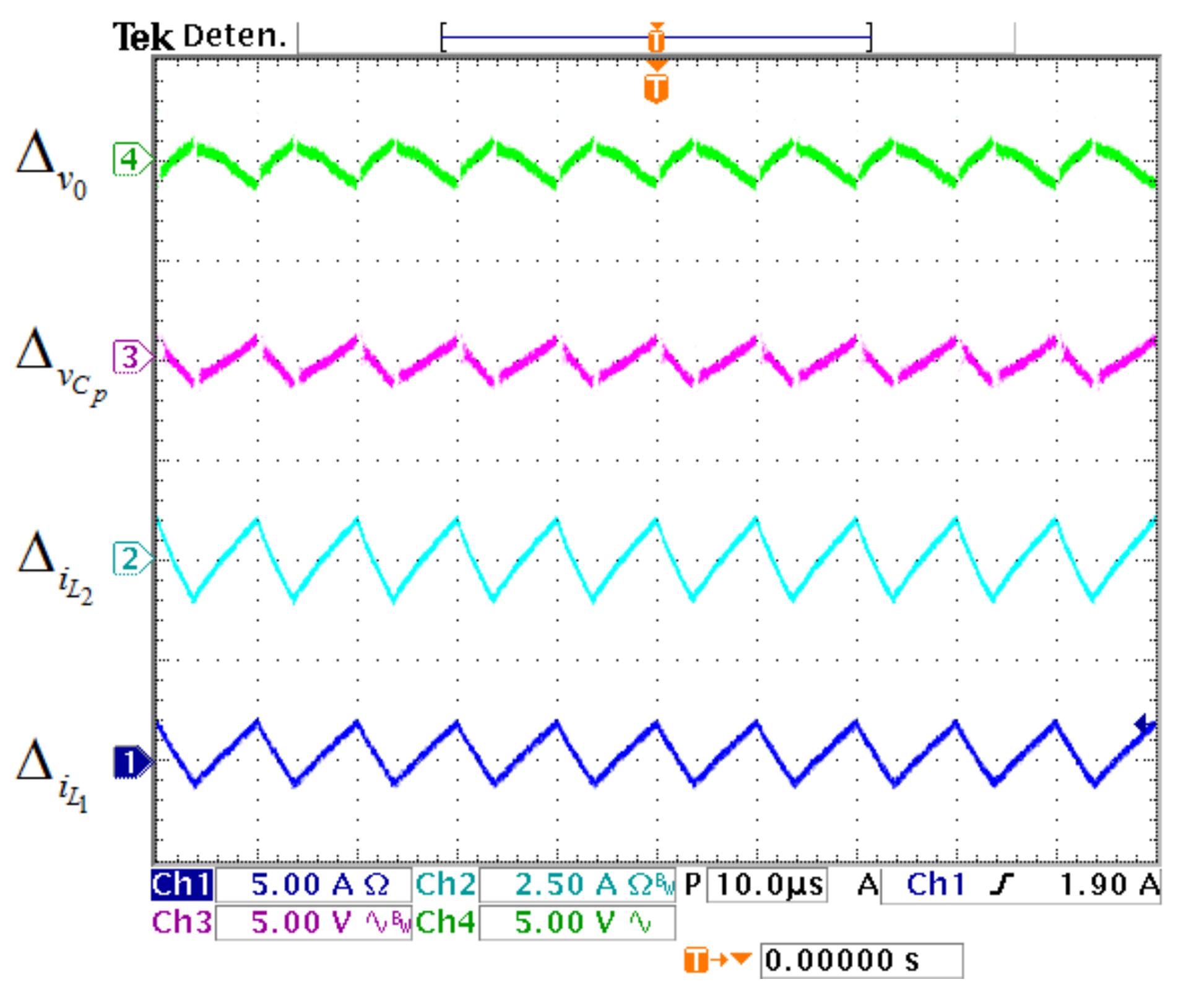
Voltage and current ripples of the prototype are exhibited in
Figure 23. The value of
is 2.8 V (1.30%), the value of
is 2.2 V (1.60%), the value of
is 1.7 A (27%), and the value of
is 3 A (17.1%).


