2D Electronics Based on Graphene Field Effect Transistors: Tutorial for Modelling and Simulation
Abstract
:1. Introduction
2. Most Common Graphene Transistor Topologies
2.1. Top-Gated Graphene Transistor
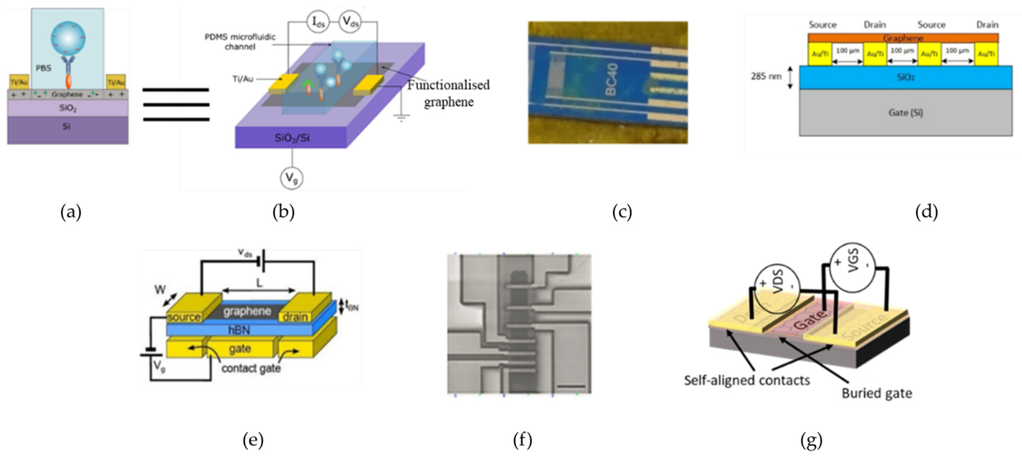
2.2. Back-Gated Graphene Transistor
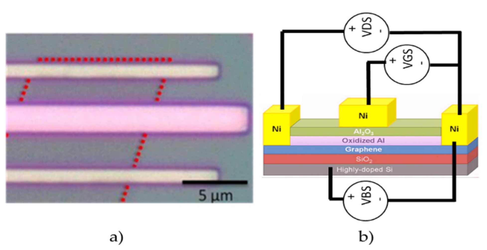
2.3. Top-/Back-Gated Transistor
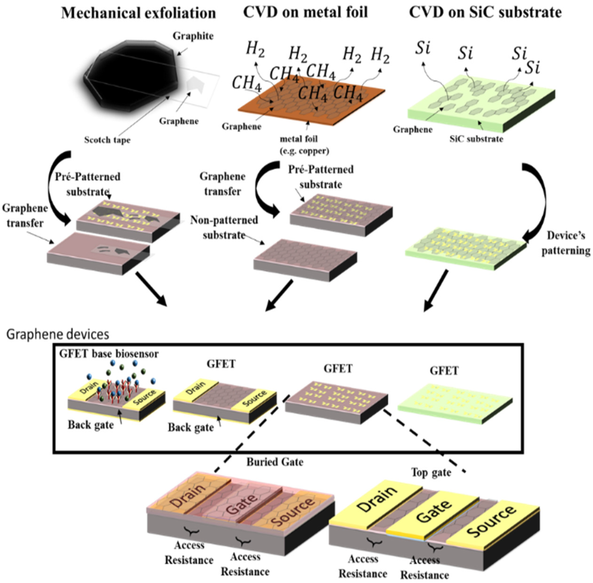
3. Fabrication Methods
3.1. Graphene Fabrication Options
3.2. Substrate for Graphene Transistors
4. Overview of Graphene Transistors
5. Performance Assessment Based on GFET Simulation
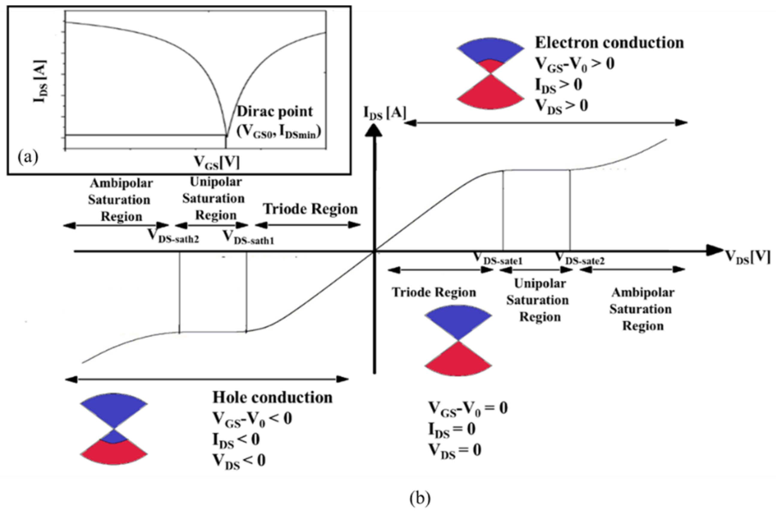
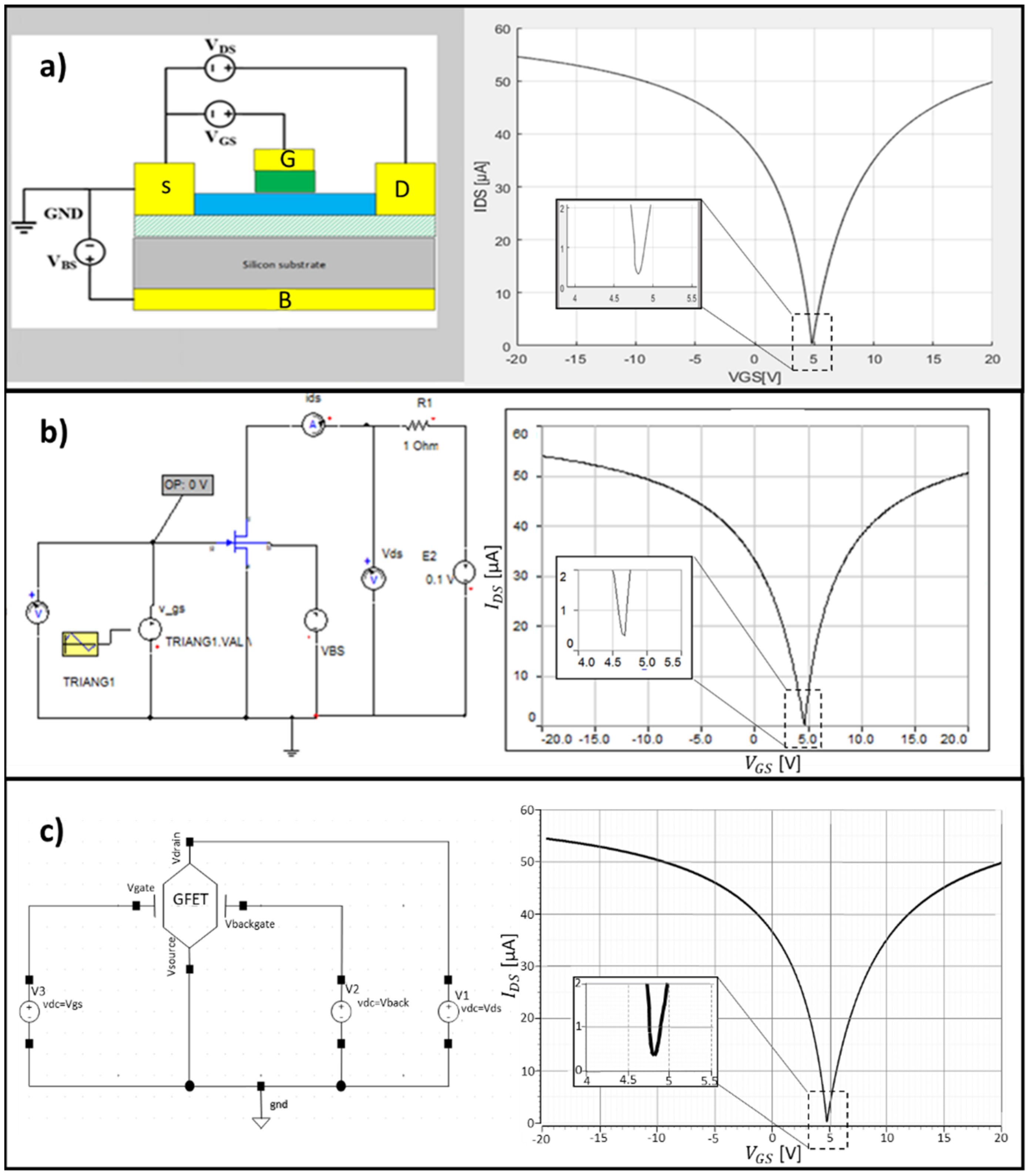
5.1. GFET Transfer Characteristic Curve
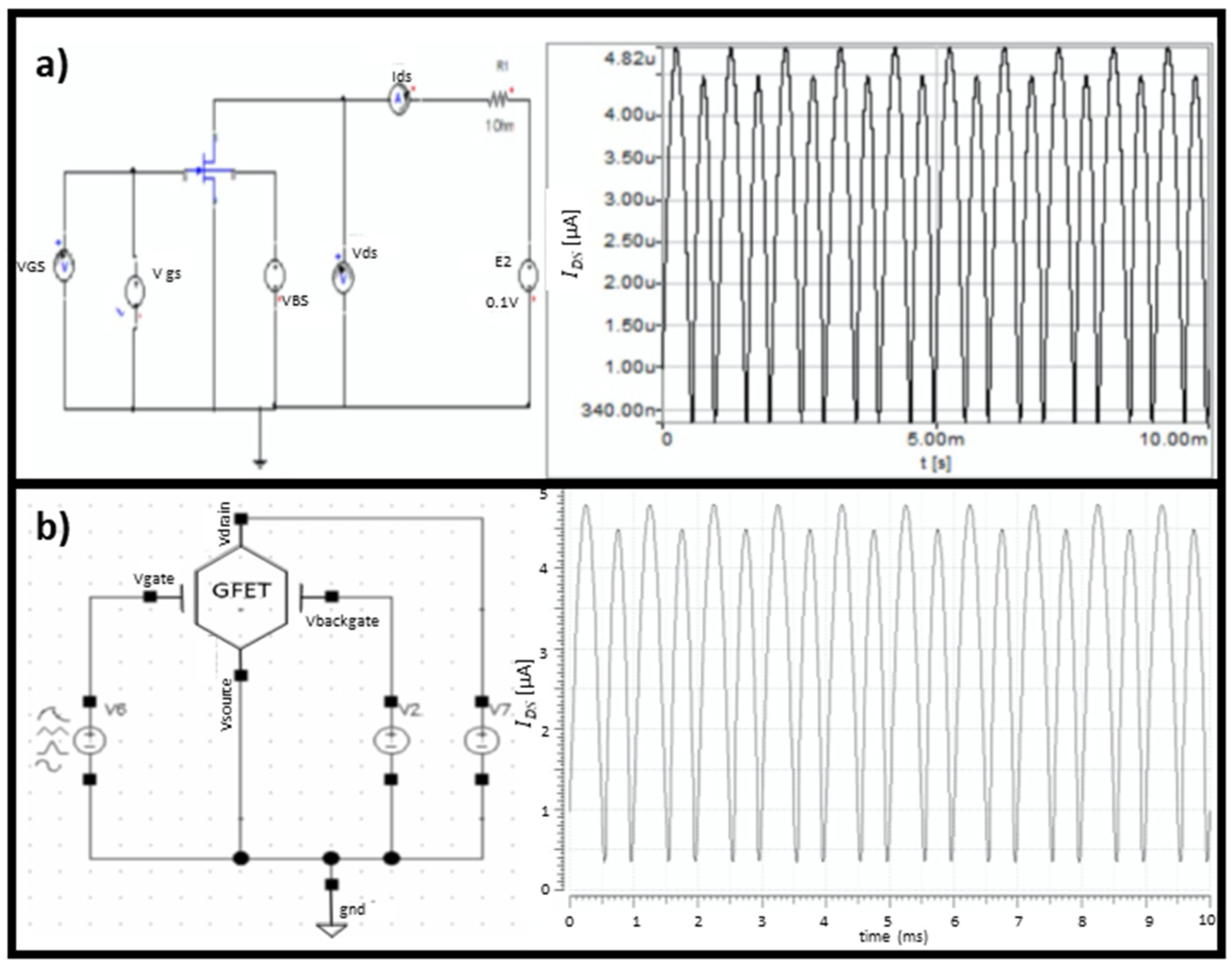
5.2. GFET Simulation Platforms
5.3. GFET Model Parameters Computation
6. Conclusions
Supplementary Materials
Funding
Conflicts of Interest
References
- Cheng, R.; Jiang, S.; Chen, Y.; Liu, Y.; Weiss, N.; Cheng, H.-C.; Wu, H.; Huang, Y.; Duan, X. Few-layer molybdenum disulfide transistors and circuits for high-speed flexible electronics. Nat. Commun. 2014, 5, 5143. [Google Scholar] [CrossRef] [PubMed]
- Novoselov, K.S.; Geim, A.K.; Morozov, S.V.; Jiang, D.; Zhang, Y.; Dubonos, S.V.; Grigorieva, I.V.; Firsov, A.A. Electric Field Effect in Atomically Thin Carbon Films. Science 2004, 306, 666–669. [Google Scholar] [CrossRef] [PubMed] [Green Version]
- Geim, A.; Novoselov, K. The rise of grapheme. Nat. Mater. 2007, 6, 183–191. [Google Scholar] [CrossRef] [PubMed]
- Katsnelson, M.I.; Novoselov, K.S.; Geim, A.K. Chiral tunnelling and the Klein paradox in grapheme. Nat. Phys. 2006, 2, 620–625. [Google Scholar] [CrossRef] [Green Version]
- Schwierz, F. Graphene transistors. Nat. Nanotechnol. 2010, 5, 487–496. [Google Scholar] [CrossRef]
- Avouris, P. Graphene: Electronic and Photonic Properties and Devices. Nano Lett. 2010, 10, 4285–4294. [Google Scholar] [CrossRef]
- Jenkins, K.A.; Lin, Y.-M.; Farmer, D.; Dimitrakopoulos, C.; Chiu, H.-Y.; Valdes-Garcia, A.; Avouris, P.; Grill, A. Graphene RF Transistor Performance. ECS Trans. 2010, 28, 3–13. [Google Scholar] [CrossRef] [Green Version]
- Novoselov, K.S.; Geim, A.K.; Morozov, S.V.; Jiang, D.; Katsnelson, M.I.; Grigorieva, I.V.; Dubonos, S.V.; Firsov, A.A. Two-dimensional gas of massless Dirac fermions in graphene. Nature 2005, 438, 197–200. [Google Scholar] [CrossRef]
- Szunerits, S.; Boukherroub, R. Graphene-based biosensors. Interface Focus 2018, 8, 20160132. [Google Scholar] [CrossRef]
- Huang, C.; Hao, Z.; Qi, T.; Pan, Y.; Zhao, X. An integrated flexible and reusable graphene field effect transistor nanosensor for monitoring glucose. J. Mater. 2020, 6, 308–314. [Google Scholar] [CrossRef]
- Gao, Q.; Li, X.; Tian, M.; Xiong, X.; Zhang, Z.; Wu, Y. Short-Channel Graphene Mixer with High Linearity. IEEE Electron Device Lett. 2017, 38, 1168–1171. [Google Scholar] [CrossRef]
- Hirai, H.; Tsuchiya, H.; Kamakura, Y.; Mori, N.; Ogawa, M. Electron mobility calculation for graphene on substrates. J. Appl. Phys. 2014, 116, 083703. [Google Scholar] [CrossRef] [Green Version]
- Bolotin, K.I.; Sikes, K.J.; Jiang, Z.; Klima, M.; Fudenberg, G.; Hone, J.; Kim, P.; Stormer, H.L. Ultrahigh electron mobility in suspended graphene. Solid State Commun. 2008, 146, 351–355. [Google Scholar] [CrossRef] [Green Version]
- Lin, Y.-M.; Dimitrakopoulos, C.; Jenkins, K.A.; Farmer, D.B.; Chiu, H.-Y.; Grill, A.; Avouris. 100-GHz Transistors from Wafer-Scale Epitaxial Graphene. Science 2010, 327, 662. [Google Scholar] [CrossRef] [Green Version]
- Wu, Y.; Lin, Y.-m.; Bol, A.A.; Jenkins, K.A.; Xia, F.; Farmer, D.B.; Zhu, Y.; Avouris, P. High-frequency, scaled graphene transistors on diamond-like carbon. Nature 2011, 472, 74–78. [Google Scholar] [CrossRef]
- Bai, J.; Liao, L.; Zhou, H.; Cheng, R.; Liu, L.; Huang, Y.; Duan, X. Top-Gated Chemical Vapor Deposition Grown Graphene Transistors with Current Saturation. Nano Lett. 2011, 11, 2555–2559. [Google Scholar] [CrossRef] [PubMed] [Green Version]
- Liao, L.; Lin, Y.-C.; Bao, M.; Cheng, R.; Bai, J.; Liu, Y.; Qu, Y.; Wang, K.L.; Huang, Y.; Duan, X. High-speed graphene transistors with a self-aligned nanowire gate. Nature 2010, 467, 305–308. [Google Scholar] [CrossRef] [PubMed]
- Guerriero, E.; Pedrinazzi, P.; Mansouri, A.; Habibpour, O.; Winters, M.; Rorsman, N.; Behnam, A.; Carrion, E.A.; Pesquera, A.; Centeno, A.; et al. High-Gain Graphene Transistors with a Thin AlOx Top-Gate Oxide. Sci. Rep. 2017, 2419, 1–7. [Google Scholar] [CrossRef] [Green Version]
- Danielson, E.; Sontakke, V.A.; Porkovich, A.J.; Wang, Z.; Kumar, P.; Ziadi, Z.; Yokobayashi, Y.; Sowwan, M. Graphene based field-effect transistor biosensors functionalized using gas-phase synthesized gold nanoparticles. Sens. Actuators B Chem. 2020, 320, 128432. [Google Scholar] [CrossRef]
- Hanna, T.; Deltimple, N.; Khenissa, M.S.; Pallecchi, E.; Happy, H.; Frégonèse, S. 2.5 GHz integrated graphene RF power amplifier on SiC substrate. Solid-State Electron. 2017, 127, 26–31. [Google Scholar] [CrossRef]
- Meric, I.; Baklitskaya, N.; Kim, P.; Shepard, K.L. RF performance of top-gated, zero-bandgap graphene field-effect transistors. In Proceedings of the 2008 IEEE International Electron Devices Meeting, San Francisco, CA, USA, 15–17 December 2008; pp. 1–4. [Google Scholar] [CrossRef]
- Ohno, Y.; Kanai, Y.; Mori, Y.; Nagase, M.; Matsumoto, K. Top-gated graphene field-effect transistors by low-temperature synthesized SiNx insulator on SiC substrates. Jpn. J. Appl. Phys. 2016, 55, 06GF09-1. [Google Scholar] [CrossRef]
- Yu, C.; He, Z.Z.; Liu, Q.B.; Song, X.B.; Xu, P.; Han, T.T.; Li, J.; Feng, Z.H.; Cai, S.J. Graphene Amplifier MMIC on SiC Substrate. IEEE Electron Device Lett. 2016, 37, 684–687. [Google Scholar] [CrossRef]
- Ping, J.; Vishnubhotla, R.; Vrudhula, A.; Johnson, A.T.C. Scalable Production of High-Sensitivity, Label Free DNA Biosensors Based on Back-Gated Graphene Field Effect Transistors. ACS Nano 2016, 10, 8700–8704. [Google Scholar] [CrossRef]
- Tsang, D.K.H.; Lieberthal, T.J.; Watts, C.; Dunlop, I.E.; Ramadan, S.; del Rio Hernandez, A.E.; Klein, N. Chemically Functionalised Graphene FET Biosensor for the Label-free Sensing of Exosomes. Sci. Rep. 2019, 9, 13946. [Google Scholar] [CrossRef] [PubMed] [Green Version]
- Park, D.; Chang, T.; Mikael, S.; Seo, J.; Nealey, P.F.; Ma, Z. Graphene RF transistors with buried bottom gate. In Proceedings of the 2013 IEEE 13th Topical Meeting on Silicon Monolithic Integrated Circuits in RF Systems, Austin, TX, USA, 21–23 January 2013; pp. 84–86. [Google Scholar] [CrossRef]
- Wang, H.; Nezich, D.; Kong, J.; Palacios, T. Graphene Frequency Multipliers. IEEE Electron Device Lett. 2009, 30, 547–549. [Google Scholar] [CrossRef]
- Liu, C.-H.; Chang, Y.-C.; Norris, T.B.; Zhong, Z. Graphene photodetectors with ultra-broadband and high responsivity at room temperature. Nat. Nanotechnol. 2014, 9, 273–278. [Google Scholar] [CrossRef] [PubMed]
- Wilmart, Q.; Boukhicha, M.; Graef, H.; Mele, D.; Palomo, J.; Rosticher, M.; Taniguchi, T.; Watanabe, K.; Bouchiat, V.; Baudin, E.; et al. High-Frequency Limits of Graphene Field-Effect Transistors with Velocity Saturation. Appl. Sci. 2020, 10, 446. [Google Scholar] [CrossRef] [Green Version]
- Han, S.; Oida, S.; Jenkins, K.A.; Lu, D.; Zhu, Y. Multifinger Embedded T-Shaped Gate Graphene RF Transistors with High fMAX/fT Ratio. IEEE Electron Device Lett. 2013, 34, 1340–1342. [Google Scholar] [CrossRef]
- Wei, W.; Mhedbhi, S.; Tilmant, P.; Happy, H.; Pallecchi, E. Towards High-Transconductance Graphene High-Speed Biosensors. In Proceedings of the IEEE International Microwave Biomedical Conference (IMBioC), Philadelphia, PA, USA, 14–15 June 2018; pp. 7–9. [Google Scholar] [CrossRef]
- Lyu, H.; Lu, Q.; Liu, J.; Wu, X.; Zhang, J.; Li, J.; Niu, J.; Yu, Z.; Wu, H.; Qian, H. Deep-submicron Graphene Field-Effect Transistors with State-of-Art fmax. Sci. Rep. 2016, 6, 35717. [Google Scholar] [CrossRef] [Green Version]
- Wang, Y.; Huang, B.-C.; Zhang, M.; Miao, C.; Xie, Y.-H.; Woo, J.C.S. Fabrication of Self-Aligned Graphene FETs with Low Fringing Capacitance and Series Resistance. Int. Sch. Res. Not. 2012, 2012. [Google Scholar] [CrossRef] [Green Version]
- Han, S.-J.; Valdes-Garcia, A.; Bol, A.A.; Franklin, A.D.; Farmer, D.; Kratschmer, E.; Jenkins, K.A. Graphene technology with inverted-T gate and RF passives on 200 mm platform. In Proceedings of the 2011 International Electron Devices Meeting, Washington, DC, USA, 5–7 December 2011; pp. 2.2.1–2.2.4. [Google Scholar] [CrossRef]
- Meric, I.; Dean, C.; Young, A.; Hone, J.; Kim, P.; Shepard, K.L. Graphene field-effect transistors based on boron nitride gate dielectrics. In Proceedings of the 2010 International Electron Devices Meeting, San Francisco, CA, USA, 6–8 December 2010; pp. 23.2.1–23.2.4. [Google Scholar] [CrossRef] [Green Version]
- Voronin, K.V.; Ermolaev, G.A.; Stebunov, Y.V.; Arsenin, A.V.; Bylinkin, A.N.; Jensen, B.B.E.; Jørgensen, B.; Volkov, V.S. Substrate effects in graphene field-effect transistor photodetectors. J. Phys. Conf. Ser. 2020, 1461, 012188. [Google Scholar] [CrossRef]
- Sarker, B.K.; Cazalas, E.; Chung, T.-F.; Childres, I.; Jovanovic, I.; Chen, Y.P. Position-dependent and millimetre-range photodetection in phototransistors with micrometre-scale graphene on SiC. Nat. Nanotechnol. 2017, 12, 668–674. [Google Scholar] [CrossRef] [PubMed] [Green Version]
- Kim, S.; Nah, J.; Jo, I.; Shahrjerdi1, D.; Colombo, L.; Yao, Z.; Tutuc, E.; Banerjee, S.K. Realization of a high mobility dual-gated graphene field-effect transistor with Al2O3 dielectric. Appl. Phys. Lett. 2009, 94, 062107. [Google Scholar] [CrossRef] [Green Version]
- Wang, Z.; Zhang, Z.; Xu, H.; Ding, L.; Wang, S.; Penga, L.-M. A high-performance top-gate graphene field-effect transistor based frequency doubler. Appl. Phys. Lett. 2010, 96, 173104. [Google Scholar] [CrossRef]
- Li, W.; Li, S.-L.; Komatsu, K.; Aparecido-Ferreira, A.; Lin, Y.-F.; Xu, Y.; Osada, M.; Sasaki, T.; Tsukagoshi, K. Realization of graphene field-effect transistor with high-κ HCa2Nb3O10 nanoflake as top-gate dielectric. Appl. Phys. Lett. 2013, 103, 023113. [Google Scholar] [CrossRef]
- Xia, F.; Farmer, D.B.; Lin, Y.M.; Avouris, P. Graphene field-effect transistors with high on/off current ratio and large transport band gap at room temperature. Nanotechnol. Lett. 2010, 10, 715–718. [Google Scholar] [CrossRef] [Green Version]
- Zhang, Z.; Xu, H.; Zhong, H.; Peng, L.-M. Direct extraction of carrier mobility in graphene field-effect transistor using current-voltage and capacitance-voltage measurements. Appl. Phys. Lett. 2012, 101, 213103. [Google Scholar] [CrossRef] [Green Version]
- Wang, H.; Taychatanapat, T.; Hsu, A.; Watanabe, K.; Taniguchi, T.; Jarillo-Herrero, P.; Palacios, T. BN/Graphene/BN Transistors for RF Applications. IEEE Electron Device Lett. 2011, 32, 1209–1211. [Google Scholar] [CrossRef] [Green Version]
- Meric, I.; Han, M.Y.; Young, A.F.; Ozyilmaz, B.; Kim, P.; Shepard, K.L. Current saturation in zero-bandgap, top-gated graphene field-effect transistors. Nat. Nanotechnol. 2008, 3, 654–659. [Google Scholar] [CrossRef]
- Barin, G.B.; Song, Y.; Gimenez, I.d.; Filho, A.G.S.; Barreto, L.S.; Kong, J. Optimized graphene transfer: Influence of polymethylmethacrylate (PMMA) layer concentration and baking time on graphene final performance. Carbon 2015, 84, 82–90. [Google Scholar] [CrossRef]
- Ramón, M.E.; Movva, H.C.P.; Chowdhury, S.F.; Parrish1, K.N.; Rai1, A.; Magnuson, C.W.; Ruoff, R.S.; Akinwande, D.; Banerjee, S.K. Impact of contact and access resistances in graphene field-effect transistors on quartz substrates for radio frequency applications. Appl. Phys. Lett. 2014, 104, 073115. [Google Scholar] [CrossRef]
- Wang, H.; Hsu, A.; Kim, K.K.; Kong, J.; Palacios, T. Gigahertz ambipolar frequency multiplier based on CVD graphene. In Proceedings of the International Electron Devices Meeting, San Francisco, CA, USA, 6–8 December 2010; pp. 23.6.1–23.6.4. [Google Scholar] [CrossRef]
- Kim, E.; Jain, N.; Xu, Y.; Yu, B. Logic Inverter Implemented with CVD-Assembled Graphene FET on Hexagonal Boron Nitride. IEEE Trans. Nanotechnol. 2012, 11, 619–623. [Google Scholar] [CrossRef]
- Han, S.-J.; Jenkins, K.A.; Garcia, A.V.; Franklin, A.D.; Bol, A.A.; Haensch, W. High-Frequency Graphene Voltage Amplifier. Nano Lett. 2011, 11, 3690–3693. [Google Scholar] [CrossRef]
- Ma, P.; Jin, Z.; Guo, J.; Pan, H.; Liu, X.; Ye, T.; Jia, Y.; Guo, L.; Chen, X. Top-gated graphene field-effect transistors on SiC substrates. Chin. Sci. Bull. 2012, 57, 2401–2403. [Google Scholar] [CrossRef] [Green Version]
- Moon, J.S.; Curtis, D.; Bui, S.; Hu, M.; Gaskill, D.K.; Tedesco, J.L.; Asbeck, P.; Jernigan, G.G.; VanMil, B.L.; Myers-Ward, R.L.; et al. Top-Gated Epitaxial Graphene FETs on Si-Face SiC Wafers With a Peak Transconductance of 600 mS/mm. IEEE Electron Device Lett. 2010, 31, 260–262. [Google Scholar] [CrossRef]
- Waldmann, D.; Jobst, J.; Speck, F.; Seyller, T.; Krieger, M.; Weber, H.B. Bottom-gated epitaxial graphene. Nat. Mater 2011, 10, 357–360. [Google Scholar] [CrossRef] [PubMed]
- Tien, D.H.; Park, J.-Y.; Kim, K.B.; Lee, N.; Seo, Y. Characterization of Graphene-based FET Fabricated using a Shadow Mask. Sci. Rep. 2016, 6, 25050. [Google Scholar] [CrossRef] [PubMed] [Green Version]
- Kathalingam, A.; Senthilkumar, V.; Rhee, J.-K. Hysteresis I–V nature of mechanically exfoliated graphene FET. J. Mater. Sci. Mater. Electron. 2014, 25, 1303–1308. [Google Scholar] [CrossRef]
- Anteroinen, J.; Kim, W.; Stadius, K.; Riikonen, J.; Lipsanen, H.; Ryynänen, J. Electrical properties of CVD-graphene FETs. In Proceedings of the 2011 NORCHIP, Lund, Sweden, 14–15 November 2011; pp. 1–4. [Google Scholar] [CrossRef]
- Gu, G.; Nie, S.; Feenstra, R.M.; Devaty, R.P.; Choyke, W.J.; Chan, W.K.; Kane, M.G. Field effect in epitaxial graphene on a silicon carbide substrate. Appl. Phys. Lett. 2007, 90, 253507. [Google Scholar] [CrossRef] [Green Version]
- Yi, M.; Shen, Z. A review on mechanical exfoliation for the scalable production of graphene. J. Mater. Chem. A 2015, 3, 11700–11715. [Google Scholar] [CrossRef]
- Wu, Y.; Zou, X.; Sun, M.; Cao, Z.; Wang, X.; Huo, S.; Zhou, J.; Yang, Y.; Yu, X.; Kong, Y.; et al. 200 GHz Maximum Oscillation Frequency in CVD Graphene Radio Frequency Transistors. ACS Appl. Mater. Interfaces 2016, 8, 25645–25649. [Google Scholar] [CrossRef] [PubMed]
- Wu, Y.Q.; Ye, P.D.; Capano, M.A.; Xuan, Y.; Sui, Y.; Qi, M.; Cooper, J.A.; Shen, T.; Pandey, D.; Prakash, G.; et al. Top-gated graphene field-effect-transistors formed by decomposition of SiC. Appl. Phys. Lett. 2008, 92, 092102. [Google Scholar] [CrossRef] [Green Version]
- Liang, Y.; Liang, X.; Zhang, Z.; Li, W.; Huoa, X.; Penga, L. High mobility flexible graphene field-effect transistors and ambipolar radio-frequency circuits. Nanoscale 2015, 7, 10954–10962. [Google Scholar] [CrossRef] [PubMed]
- Lu, C.-C.; Lin, Y.-C.; Yeh, C.-H.; Huang, J.-C.; Chiu, P.-W. High Mobility Flexible Graphene Field-Effect Transistors with Self-Healing Gate Dielectrics. ACS Nano 2012, 6, 4469–4474. [Google Scholar] [CrossRef] [PubMed]
- He, Y.-L.; Liu, J.-B.; Wen, T.-L.; Yang, Q.-H.; Feng, Z.; Tan, W.; Li, X.-S.; Wen, Q.-Y.; Zhang, H.-W. Flexible terahertz modulators based on graphene {FET} with organic high-k dielectric layer. Mater. Res. Express 2018, 5, 115607. [Google Scholar] [CrossRef]
- Cabral, P.D.; Domingues, T.; Machado, G.; Chicharo, A.; Cerqueira, F.; Fernandes, E.; Athayde, E.; Alpuim, P.; Borme, J. Clean-Room Lithographical Processes for the Fabrication of Graphene Biosensors. Materials 2020, 13, 5728. [Google Scholar] [CrossRef]
- Umoh, I.J.; Kazmierski, T.J.; Al-Hashimi, B.M. A Dual-Gate Graphene FET Model for Circuit Simulation—SPICE Implementation. IEEE Trans. Nanotechnol. 2013, 12, 427–435. [Google Scholar] [CrossRef]
- Umoh, I.J. Graphene FET Circuit-Level Device Modelling. Ph.D. Thesis, University of Southampton, Southampton, UK, June 2014. [Google Scholar]
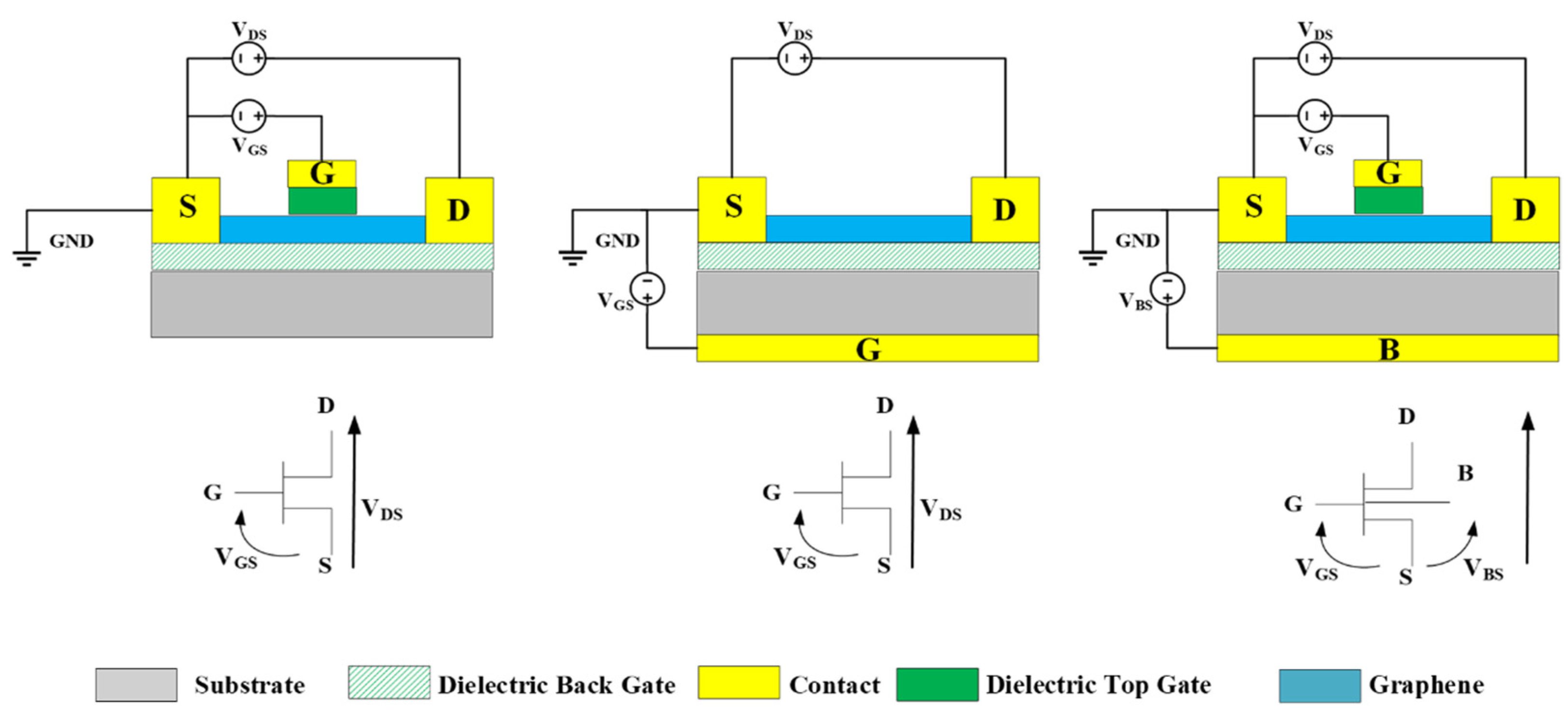
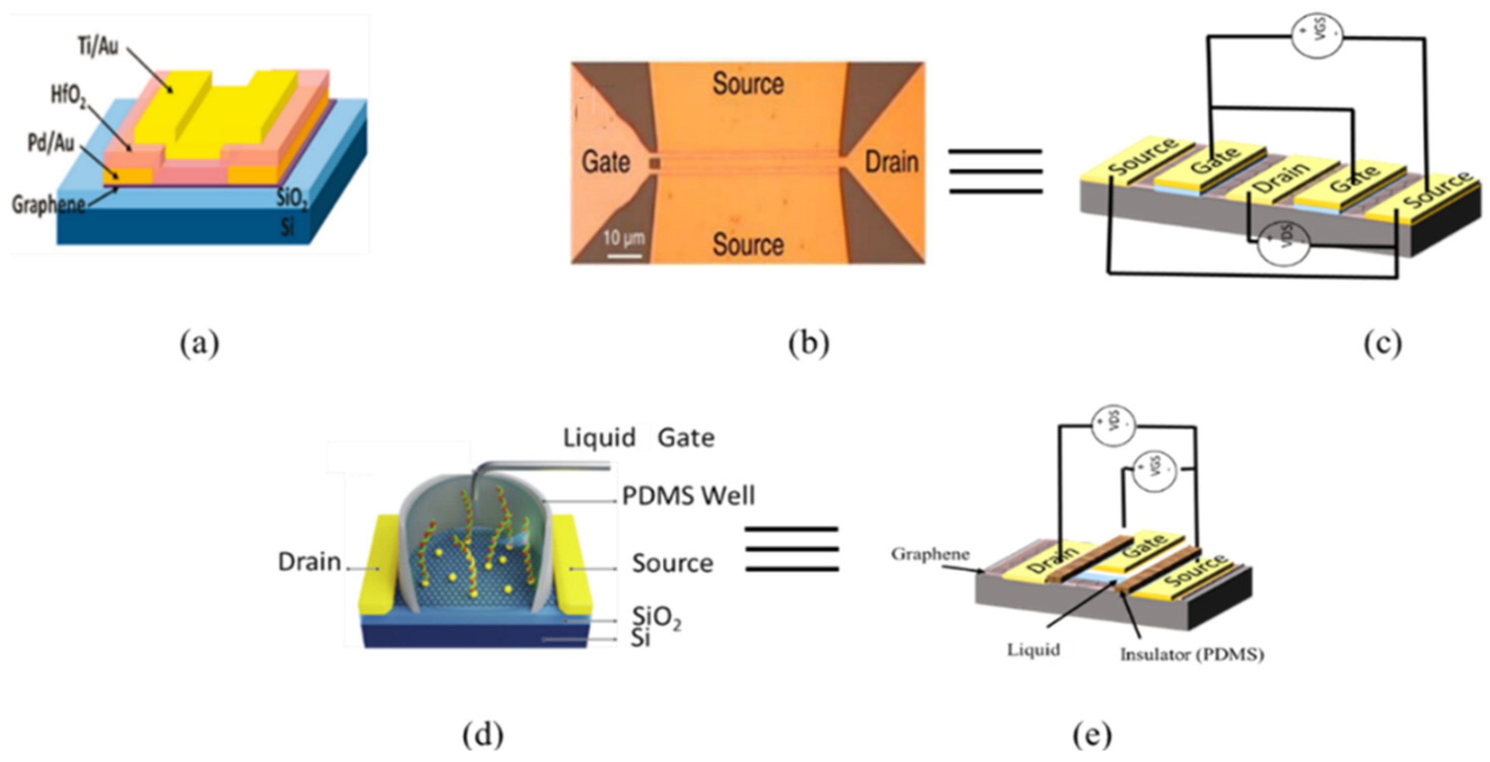
| Purpose | Graphene Type | Differentiating Approach | Performance | Ref |
|---|---|---|---|---|
| Achieve high transconductance and drain-current saturation in GFETs | CVD | Self-aligned source/drain electrodes | Maximum of 250 µS/µm | [16] |
| GFET for RF applications | Mechanical exfoliation | Nanowire as the gate of the graphene transistor; self-aligned source/drain electrodes | Maximum of 1.27 mS/µm Intrinsic fT 300 GHz | [17] |
| Improve the drain-current saturation increasing the gain in RF transistors | CVD | Thin gate oxide dielectric (~4 nm) | > 3 | [18] |
| DNA biosensor | CVD | Use of a liquid gate and PDMS well to isolate source/drain electrodes from the liquid gate | Detection of full hybridization of the complementary strand down to 15 aM | [19] |
| Graphene RF power amplifier | Grown by CVD on SiC substrate | Dual top gate | Power amplifier gain of 8.9 dB at 2.5 GHz | [20] |
| GFET for RF applications | Mechanical exfoliation | Dual top gate | Maximum of 550 µS/µm Intrinsic14.7 GHz | [21] |
| Study of the low-temperature deposition of gate oxides in GFETs | Grown by CVD on SiC substrate | Low temperature deposition of by Cat-CVD | No gate current leakage | [22] |
| GFET for RF applications | CVD | T-shaped gate and drain/source; self-aligned source/drain electrodes | Intrinsic Extrinsic | [23] |
| Purpose | Graphene Type | Differentiating Approach | Performance | Ref |
|---|---|---|---|---|
| High-sensitivity label-free DNA biosensors | CVD |
| Detection limit depends on the length of the DNA, for 60-mer DNA the detection limit is 1 fM. | [24] |
| Graphene FET biosensor for the label-free sensing of exosomes | CVD | Back-gate contact made with silver conductive paint | Exosome detection of at least 0.1 μg/mL | [25] |
| Fabrication of graphene frequency multipliers | Mechanical exfoliation | Back gate on doped silicon wafer | Able to work with 10 kHz input frequencies | [26] |
| Photodetectors | CVD | Multilayer graphene to transport charges and to absorb light. | Photodetection from the visible to the mid-infrared range, with mid-infrared responsivity higher than 1 AW−1 | [27] |
| Substrate effects on GFET photodetectors | Electrochemical delamination | Use of different semiconducting substrates | ---- | [28] |
| Study of velocity saturation graphene FETs: design and performance | Pulsed CVD | Use of the h-BN as a gate oxide. Dual-gate device for RF characterization. | > 5 in Zenner–Klein regime | [29] |
| Achieve a high | CVD | Buried gates with depth-to-with ratio up to sixfold to reduce gate resistance | Intrinsic 35 GHz and | [30] |
| Increase the transconductance for high-speed biosensors | CVD | Exposed graphene to enable the functionalization with biomolecules | Extrinsic 22 GHz and = 16 mS | [31] |
| RF graphene transistor with a high | CVD | T-gate structure to reduce the gate resistance | Extrinsic 11.4 GHz and | [32] |
| Comparison between top and buried gates and their effect on fringing capacitance | CVD | Self-aligned buried gates | Low fringing capacitance in buried gates | [33] |
| Graphene integrated frequency multiplier | CVD | Inverted T-gate to reduce the gate resistance and development of an IC using a 200 nm platform | Frequency multiplayer gain of ~−25 dB at an input of 1 GHz | [34] |
| GFET with h-BN as a gate dielectric and support material for GFETs | --- | h-BN as a gate dielectric | Intrinsic transconductance above 400 mS/mm | [35] |
| Improvement of the process-induced mobility degradation of graphene | CVD | Development of buried bottom gates | ratio of 5.31 Maximum of 6.85 µS/µm Intrinsic 2 GHz and | [36] |
| Photodetectors | Grown by CVD on SiC substrate | Back gate to modulate graphene conductivity | Non-local, position-sensitive, and large-area photodetection. | [37] |
| Purpose | Graphene Type | Fabrication Techniques | Performance | Ref |
|---|---|---|---|---|
| GFET | Mechanical exfoliation | Gate oxide (Al2O3) deposited by ALD viaprior metallization of Al. | Preservation of the graphene mobility after the gate dielectric deposition (8000 cm2/Vs) | [38] |
| GFET top-gated-based frequency doubler | Mechanical exfoliation | Yttrium oxide as a gate dielectric | Able to work with 200 kHz input frequencies | [39] |
| GFET fabricated with HCa2Nb3O10 nanoflakes as a gate dielectric | Mechanical exfoliation | Use of HCa2Nb3O10 nanoflakes | High top-gate capacitance, small top-gate current leakage | [40] |
| GFET with high Ion/Ioff ratio and large transport bandgap | Purchased bilayer graphene (mechanical exfoliation) | Gate oxide of HfO2 deposited by a prior deposition of an organic seed | Ion/Ioff ratio≈100 Electrical band gap > 130 meV | [41] |
| GFET to extract the carrier mobility of graphene | Mechanical exfoliation | Yttrium oxide as gate dielectric | -------- | [42] |
| GFET for RF electronics | Mechanical exfoliation | h-BN used as top and back gate dielectric | Current density of 1.2 A/mm Extrinsic fT = 33 GHz | [43] |
| Purpose | Graphene Type | Ref |
|---|---|---|
| CVD using metal foil substrate | Top | [47] |
| Back | [48] | |
| Back | [49] | |
| CVD on SIC | Top | [50] |
| Top | [51] | |
| Back | [52] | |
| Mechanical exfoliation | Top | [38] |
| Back | [53] | |
| Back | [54] |
| Application | Topologies | Substrate | Fabrication Complexity | ||||
|---|---|---|---|---|---|---|---|
| Top-Gate | Back-Gate | Top-/Back-Gate | Si/SiO2 | SiC | Quartz/Glass | ||
| RF applications | +++ | +++ | +++ | ++ | ++ | +++ | +++ |
| Biosensors | − | +++ | +− | +++ | ++ | +− | +++ |
| Optics | − | +++ | − | ++ | ++ | +++ | ++ |
Publisher’s Note: MDPI stays neutral with regard to jurisdictional claims in published maps and institutional affiliations. |
© 2021 by the authors. Licensee MDPI, Basel, Switzerland. This article is an open access article distributed under the terms and conditions of the Creative Commons Attribution (CC BY) license (https://creativecommons.org/licenses/by/4.0/).
Share and Cite
Jmai, B.; Silva, V.; Mendes, P.M. 2D Electronics Based on Graphene Field Effect Transistors: Tutorial for Modelling and Simulation. Micromachines 2021, 12, 979. https://doi.org/10.3390/mi12080979
Jmai B, Silva V, Mendes PM. 2D Electronics Based on Graphene Field Effect Transistors: Tutorial for Modelling and Simulation. Micromachines. 2021; 12(8):979. https://doi.org/10.3390/mi12080979
Chicago/Turabian StyleJmai, Bassem, Vitor Silva, and Paulo M. Mendes. 2021. "2D Electronics Based on Graphene Field Effect Transistors: Tutorial for Modelling and Simulation" Micromachines 12, no. 8: 979. https://doi.org/10.3390/mi12080979
APA StyleJmai, B., Silva, V., & Mendes, P. M. (2021). 2D Electronics Based on Graphene Field Effect Transistors: Tutorial for Modelling and Simulation. Micromachines, 12(8), 979. https://doi.org/10.3390/mi12080979


