Article

Improvement of Fermi-Level Pinning and Contact Resistivity in Ti/Ge Contact Using Carbon Implantation

1
Department of Electrical Engineering, Pohang University of Science and Technology (POSTECH), Pohang 37673, Korea
2
Research and Development Department, Innovative General Electronic Sensor Technology Co., Ltd. (IGEST), Pohang 37673, Korea
3
Department of Electrical Engineering, Gyeongsang National University, Jinju 52828, Korea
*
Author to whom correspondence should be addressed.
Micromachines 2022, 13(1), 108; https://doi.org/10.3390/mi13010108
Submission received: 16 December 2021 / Revised: 3 January 2022 / Accepted: 8 January 2022 / Published: 10 January 2022
(This article belongs to the Special Issue Doping Techniques in Emerging Semiconductors and Devices)

Abstract

:
Effects of carbon implantation (C-imp) on the contact characteristics of Ti/Ge contact were investigated. The C-imp into Ti/Ge system was developed to reduce severe Fermi-level pinning (FLP) and to improve the thermal stability of Ti/Ge contact. The current density (J)-voltage (V) characteristics showed that the rectifying behavior of Ti/Ge contact into an Ohmic-like behavior with C-imp. The lowering of Schottky barrier height (SBH) indicated that the C-imp could mitigate FLP. In addition, it allows a lower specific contact resistivity (ρc) at the rapid thermal annealing (RTA) temperatures in a range of 450–600 °C. A secondary ion mass spectrometry (SIMS) showed that C-imp facilitates the dopant segregation at the interface. In addition, transmission electron microscopy (TEM) and electron energy loss spectroscopy (EELS) mapping showed that after RTA at 600 °C, C-imp enhances the diffusion of Ge atoms into Ti layer at the interface of Ti/Ge. Thus, carbon implantation into Ge substrate can effectively reduce FLP and improve contact characteristics.

1. Introduction

As a channel material for the next-generation field-effect transistors (FETs), Germanium (Ge) is considered a promising alternative to silicon (Si) owing to its higher carrier mobility and the process compatibility with the advanced Si microfabrication. However, the low-solid solubility and the high-diffusion coefficient of n-type dopants in Ge hinder the realization of low specific contact resistivity (ρc) [1]. Moreover, Fermi-level pinning (FLP) caused by the metal-induced gap states (MIGS) at the metal/Ge interface is another problem to be solved [2,3,4,5]. FLP strongly occurs near the Ge valence band (Ev) and forces the electron Schottky barrier height (e-SBH) above 0.5 eV irrespective of the metal workfunction [6]. Several approaches, including dopant segregation [7], dipole formation [8], and surface treatment [9] were proposed to mitigate FLP phenomena. Recently, the use of an ultra-thin insulator between the metal and Ge showed an effective reduction of FLP but the degradation of ρc due to a high tunneling resistance [10,11,12,13]. The formation of metal germanide can be another approach because the MIGS from metal dangling bond states in germanide can lead to an FLP reduction [14,15].
Ion implantation is another approach to achieving low ρc and suppressing dopant-diffusion behaviors. For example, Germanium implantation before silicidation induces surface amorphization to aid an epitaxial regrowth on the semiconductor surface [16]. Carbon implantation (C-imp) has been introduced in Ni-silicide and Ni-germinide contacts to reduce contact resistivity [17,18]. However, Ti/Ge contact with carbon implantation has been rarely reported.
Here, we investigated the effects of C-imp on the FLP reduction of a Ti/Ge contact and the related contact characteristics. Electrical characteristics were measured using the multiring-circular transmission line model (MR-CTLM) structure and Schottky barrier diode (SBD). Physical and structural properties of Ti/Ge contact with C-imp were analyzed using scanning electron microscopy (SEM), transmission electron microscopy (TEM), electron energy loss spectroscopy (EELS), and secondary ion mass spectrometry (SIMS).

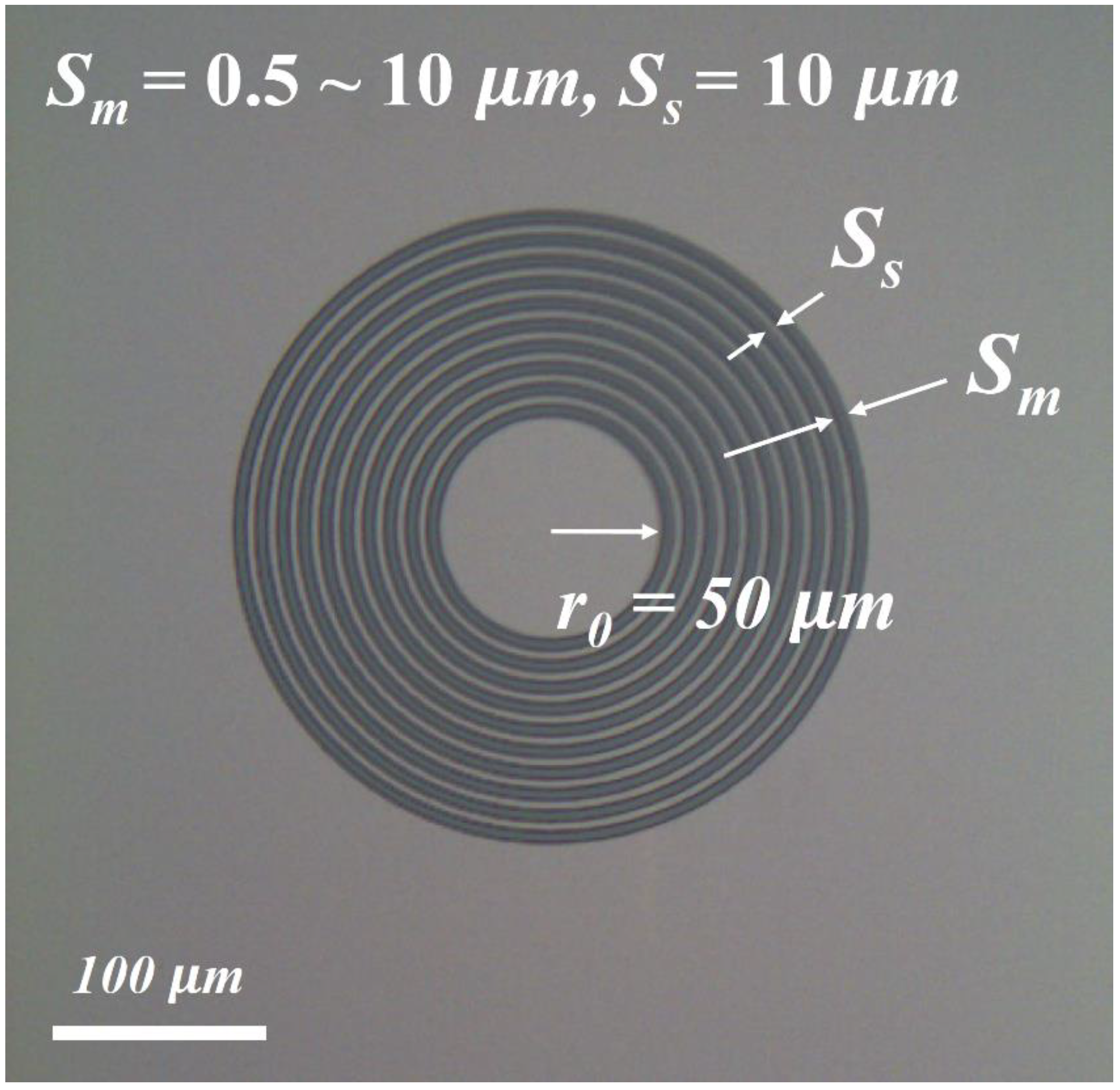
2. Materials and Methods
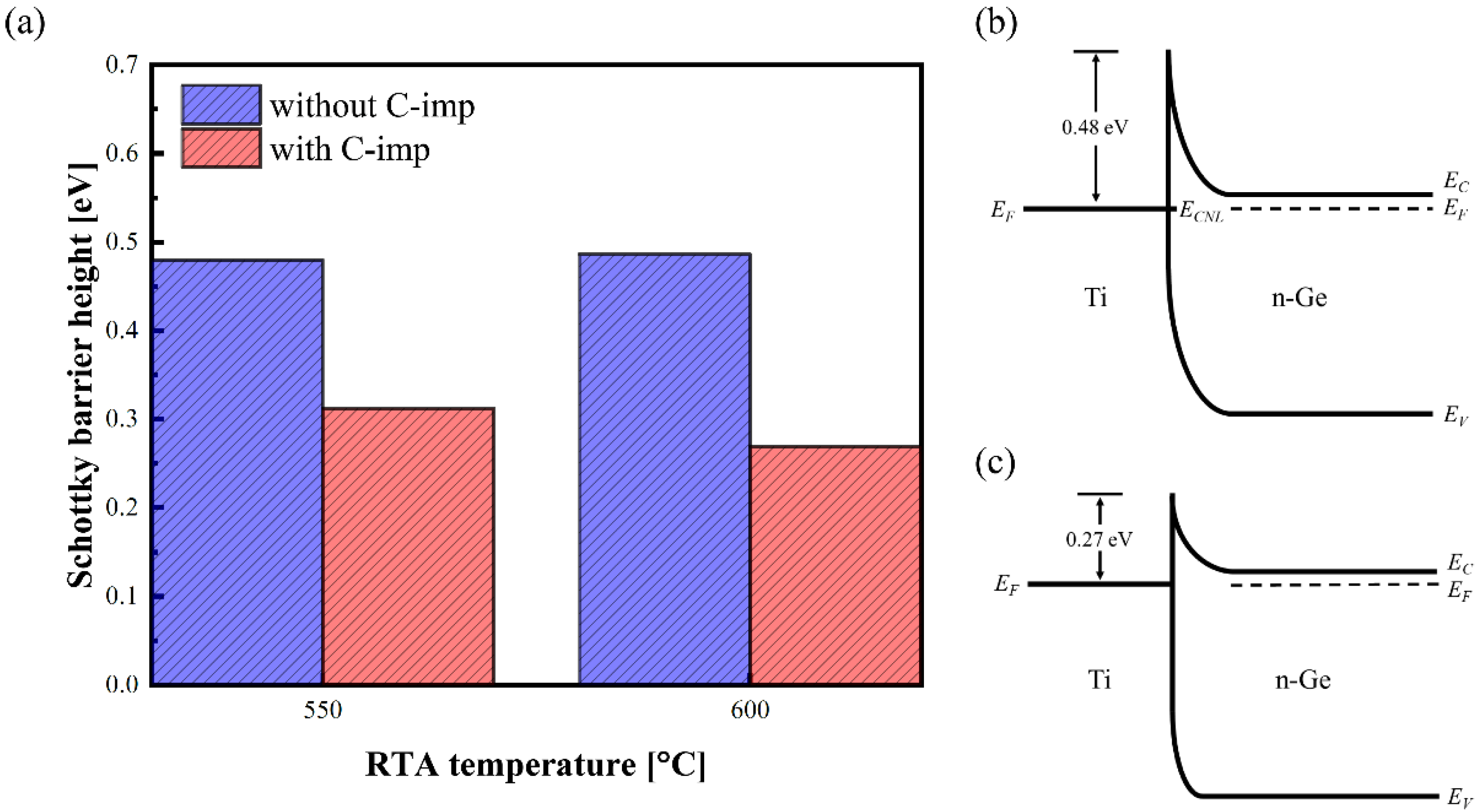
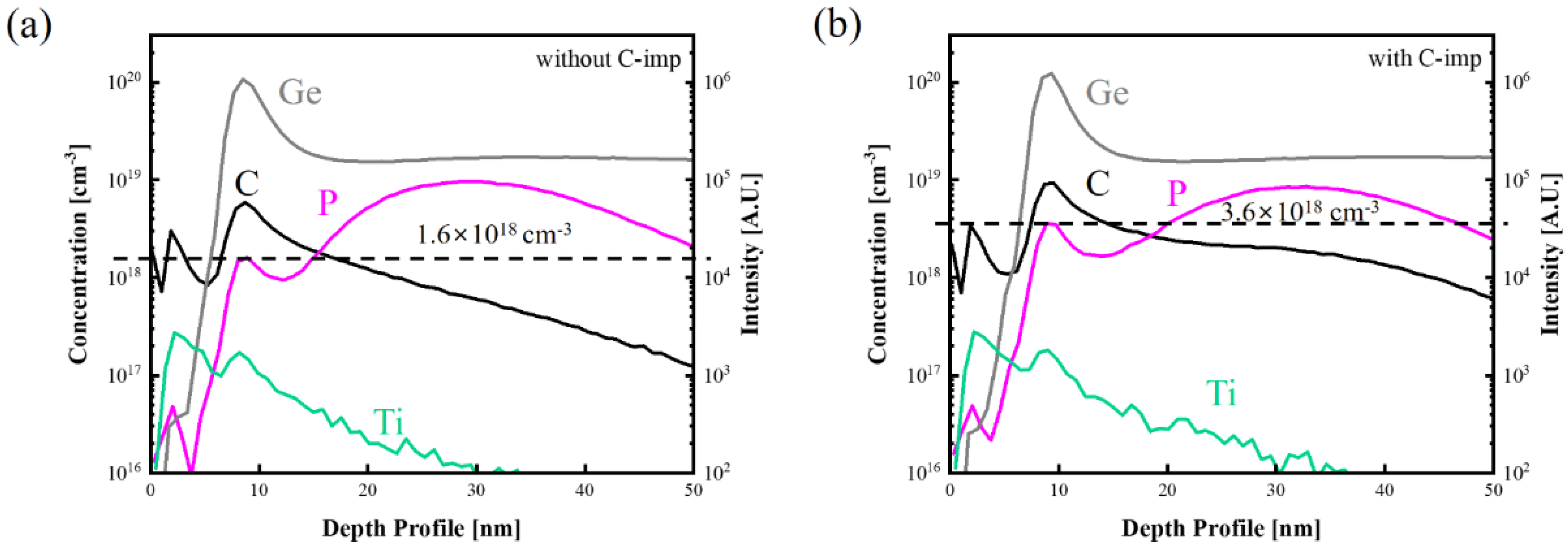
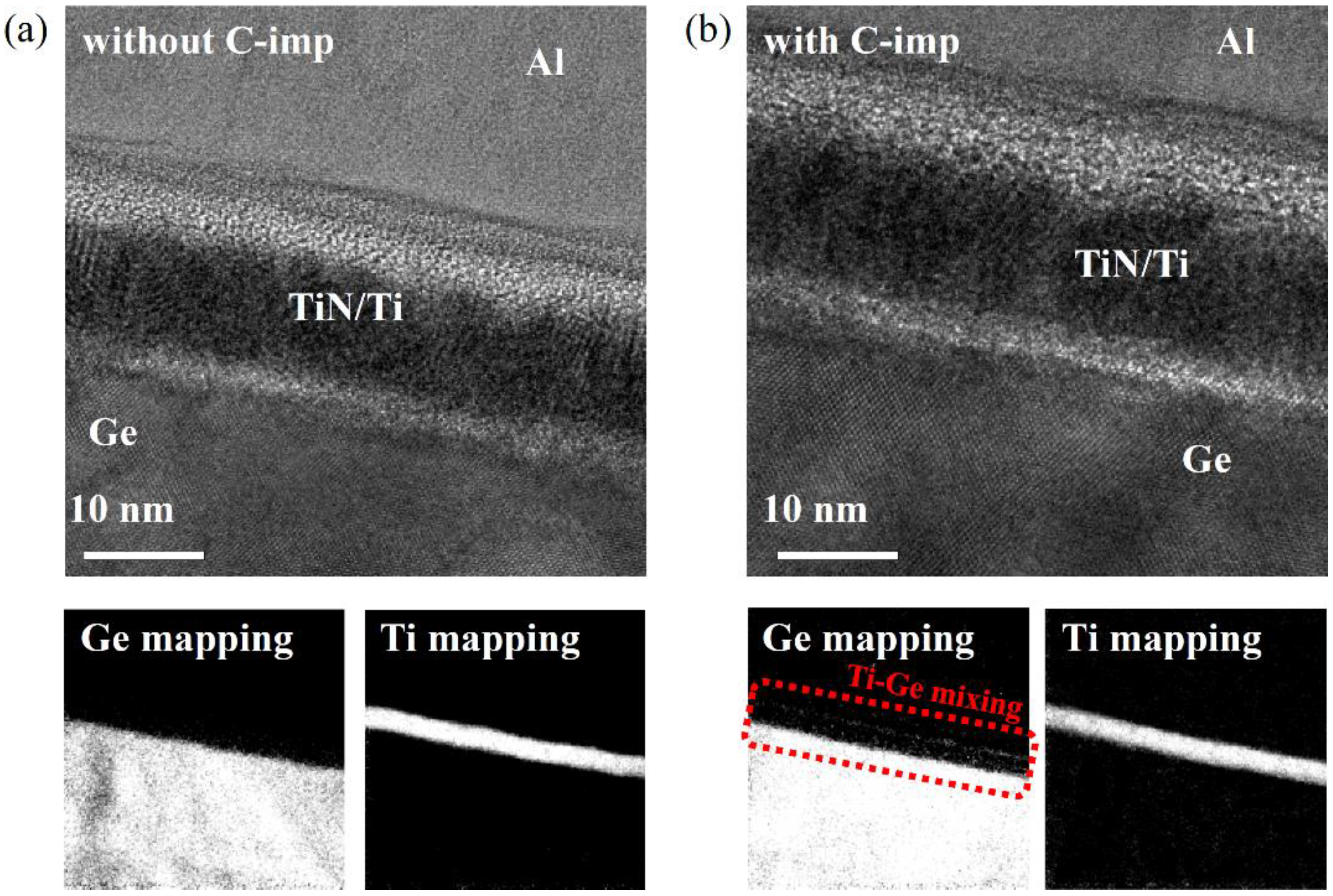
N-type Ge wafers moderately doped with phosphorus (~1018 cm−3) were cleaned in a 1:100 diluted HF (dHF) solution and deionized (DI) water to remove native oxide. Subsequently, C+ ions were implanted into the Ge substrate at a dose of 1 × 1015 cm−2 and an implantation energy of 10 keV. A reference sample without C-imp was also prepared. A SBD of Ti/Ge structure and a MR-CTLM structure were fabricated on the Ge substrate to characterize electrical properties. First, a 100 nm thick SiO2 was deposited to isolate the contact holes using a plasma-enhanced chemical vapor deposition (PECVD). Then, the metal contact was formed using the conventional photolithography process. Sequentially, the oxide was etched using a dry etcher, and a Ti (5 nm)/TiN (5 nm) was deposited using a DC sputtering system. After a metal lift-off process, rapid thermal annealing (RTA) was performed in N2 ambient for 60 s at 450–600 °C. Finally, a 100 nm thick Al was deposited as contact pad metal. The electrical measurements of current (I)–bias voltage (V) were performed using Keithley 4200-SCS. TEM images of the Ti/Ge structure without and with C-imp were obtained using a JEOL JEM 2200FS with an image Cs-corrector.

3. Results

Figure 1 shows the J-V characteristics of the Ti/Ge contacts with and without C-imp at RTA temperatures in a range of 450–600 °C for 60 s in N2 ambient. The Ti/Ge contact without C-imp shows a typical rectifying behavior attributed to a strong FLP near the Ev, which leads to a significantly high e-SBH and reduces the reverse current density. On the other hand, the Ti/Ge contact with C-imp shows an Ohmic-like behavior with relatively high current density under the reverse regime, indicating the alleviation of FLP.
Figure 2a shows the extracted e-SBHs of the Ti/Ge contacts without (blue box) and with (red box) C-imp after RTA at 550 °C and 600 °C, respectively, for 60 s in N2 ambient. The e-SBHs were extracted from the current-temperature (I-T) curves in a range of 300–378 K. The I-V relationship of a Schottky barrier diode is represented by [19]
I = A A * T 2 e q B / k T ( e q V / n k T 1 ) = I S 1 e q B / k T ( e q V / n k T 1 ) = I S ( e q V / n k T 1 )
where Is is the saturation current, A is the diode area, A* = 4πqk2m*/h3 = 120 (m*/m) A/cm2∙K2 Richardson’s constant, ΦB is the barrier height, and n is the ideality factor. For V k T / q Equation (1) can be written as follows:
ln ( I / T 2 ) = ln ( AA * ) q ( B V / n ) / k T
B = V n k q d [ ln ( I / T 2 ) ] d ( 1 / T ) = V n 2.3 k q d [ log ( I / T 2 ) ] d ( 1 / T )
Therefore, the barrier height is calculated from the slope (=d[ln(I/T2)]/d(1/T)). The bandgap and electron affinity in eV of Ge at 300 K are 0.66 and 4.0 eV, respectively. The workfunction of Ti metals is about 4.3 eV. When Fermi level is pinned near Ev of Ge, ΦB of ~0.6 eV is calculated. If there is negligible FLP, ΦB of ~0.3 eV is obtained.
Without C-imp, the SBH of ~0.48 eV was obtained for both 550 °C and 600 °C RTA, indicating the occurrence of FLP. In contrast, the SBH with C-imp was significantly reduced from 0.31 eV at 550 °C to 0.27 eV at 600 °C.
Figure 2b,c show schematics of the energy band diagrams for Ti/Ge contacts. Without C-imp, Fermi-level on the Ti side is pinned with the charge neutrality level (ECNL) due to FLP [6].
Figure 3 shows a top-view SEM image of the fabricated MR-CTLM structure to extract ρc and the sheet resistance beneath the metal (RS). The current flows through multiple metal-semiconductor structures from the center region to the outer-circle region. From the I-V curve of MR-CTLM, the total resistance (Rtot) is expressed as the sum of the effective resistance (Reff) and the parasitic resistance (Rpr) as follows [20]:
R t o t = R e f f + R p r
R e f f = R s 2 π i = 0 9 [ ln ( r i + S m r i ) + L t ( 1 r i + 1 r i + S m ) ]
R p r = R m 2 π [ i = 1 9 ln ( r i L t r i S s + L t ) ]
where r0~r9 are the inner radius of the serial CTLM. Sm and Ss are the spacing among metal rings and dielectric rings, respectively. Lt is the transfer length. Ss = 10 μm, r0 = 50 μm, and Sm, from 0.5 to 10 μm were defined using an i-line stepper. ρc was calculated from the Lt ( = ρ c / R s ) which was extracted by fitting a set of Rt-Sm data using Equations (4)–(6).
Figure 4 shows the extracted ρc values versus RTA temperature. ρc was obtained using a MR-CTLM test structure [20]. A relatively high ρc value seems mainly because of the low activation of a substrate doping concentration of ~1 × 1018 cm−3 [21,22]. After RTA annealing at 600 °C, the ρc values of the Ti/Ge with and without C imp were 1.3 × 10⁻⁵ and 8.4 × 10⁻⁴ Ω∙cm2, respectively. Owing to the FLP effect, the Ti/Ge contact without C-imp shows ρc values higher than 1.0 × 10⁻⁴ Ω∙cm2.
To further analyze the effect of C-imp on the Ti/Ge composition, TEM and SIMS were conducted. The decrease of ρc is mainly attributed to the dopant segregation in the Ti/Ge interface [23]. In particular, for the Ti/Ge contact with C-imp after RTA at 600 °C, a further reduction of ρc is observed. These results can be expected by TiGex formation. The low resistive C54-TiGex is formed at a temperature above 600 °C [24], which mitigates FLP and improves the contact resistivity [14,15].
Figure 5a,b show SIMS profiles for Ti/Ge contacts without and with C-imp, respectively. At the Ti/Ge interface with C-imp, the peak P concentration increases from 1.6 × 1018 cm−3 to 3.6 × 1018 cm−3, attributed to the dopant segregation facilitated by carbon [18]. This dopant segregation can increase the tunneling current by reducing the depletion thickness at the interface and lowering the contact resistivity.
To directly observe the microstructure of Ti/Ge contact, the cross-sectional TEM images and the corresponding EELS were analyzed. The samples were prepared after RTA at 600 °C for 60 s in N2 ambient, as shown in Figure 6. In EELS maps, a bright region represents the area that the element of interest is abundant. With C-imp, Ge element is considerably observed in the Ti layer (red box in Figure 6b). The diffused Ge reacts with Ti and forms the Ti-germanide during the RTA process, which is beneficial to reduce the contact resistivity [14,15]. These results show that the C-imp is a promising approach to lower the contact resistivity in Ti/Ge contact by inducing the dopant segregation and Ge diffusion into the Ti layer.

4. Conclusions

We investigated the electrical and material characteristics of a Ti/Ge contact with C-imp. The current-voltage behavior shows that the carbon implantation changes the Ti/Ge rectifying behavior into an Ohmic-like behavior above RTA at 450 °C. The extracted Schottky barrier height was also decreased due to the mitigation of Fermi-level pinning. The specific contact resistivity of the Ti/Ge contact with C-imp was significantly reduced by approximately two orders of magnitude. Transmission electron microscopy and secondary ion mass spectrometry showed that carbon element at the Ti/Ge interface facilitates the dopant segregation and induces the diffusion of Ge into Ti layer. Therefore, the carbon implantation is promising to improve the Ti/Ge contact properties for high-performance Ge-FET applications.

Author Contributions

Conceptualization, I.P.; investigation, D.L.; methodology, J.K.; data curation, B.J.; writing-original draft preparation, I.P. and J.-S.L.; writing-review & editing, I.P. and J.-S.L.; supervision, J.-S.L. All authors have read and agreed to the published version of the manuscript.

Funding

This work was supported by the Future Semiconductor Device Technology Development Program (10067739), funded by Ministry of Trade, Industry & Energy (MOTIE) and Korea Semiconductor Research Consortium (KSRC) and by Food, Agriculture, Forestry, and Fisheries (IPET) through the Animal Disease Management Technology Development Program, which is funded by the Ministry of Agriculture, Food, and Rural Affairs (MAFRA) (120091-02-1-CG000) and by National R&D Program through the National Research Foundation of Korea (NRF) funded by Ministry of Science and ICT (2020M3H2A1078045).

Conflicts of Interest

The authors declare no conflict of interest.

References

  1. Simoen, E.; Claeys, C. Germanium-Based Technologies, 1st ed.; Elsevier: Oxford, UK, 2007; pp. 67–96. [Google Scholar]
  2. Mönch, W. Barrier heights of real Schottky contacts explained by metal-induced gap states and lateral inhomogeneities. J. Vac. Sci. Technol. B 1999, 17, 1867–1876. [Google Scholar] [CrossRef]
  3. Nishimura, T.; Kita, K.; Toriumi, A. Evidence for strong Fermi-level pinning due to metal-induced gap states at metal/germanium interface. Appl. Phys. Lett. 2007, 91, 123123. [Google Scholar] [CrossRef]
  4. Tersoff, J. Schottky barriers and semiconductor band structures. Phys. Rev. B 1985, 32, 6968–6971. [Google Scholar] [CrossRef] [PubMed]
  5. Robertson, J.; Guo, Y.; Zhang, Z.; Li, H. Extending the metal-induced gap state model of Schottky barriers. J. Vac. Sci. Technol. B 2020, 38, 042208. [Google Scholar] [CrossRef]
  6. Dimoulas, A.; Tsipas, P.; Sotiropoulos, A.; Evangelou, E.K. Fermi-level pinning and charge neutrality level in germanium. Appl. Phys. Lett. 2006, 89, 252110. [Google Scholar] [CrossRef]
  7. Tong, Y.; Liu, B.; Lim, P.S.Y.; Yeo, Y. Selenium Segregation for Effective Schottky Barrier Height Reduction in NiGe/n–Ge contacts. IEEE Electron Device Lett. 2012, 33, 773–775. [Google Scholar] [CrossRef]
  8. Wang, J.; Huang, W.; Xu, J.; Li, J.; Huang, S.; Li, C.; Chen, S. Schottky barrier height modulation effect on n-Ge with TaN contact. Mater. Sci. Semicond. Process. 2019, 91, 206–211. [Google Scholar] [CrossRef]
  9. Kim, G.; Kim, J.; Kim, S.; Jo, J.; Shin, C.; Park, J.; Saraswat, K.C.; Yu, H. Specific Contact Resistivity Reduction Through Ar Plasma-Treated TiO2−x Interfacial Layer to Metal/Ge Contact. IEEE Electron Device Lett. 2014, 35, 1076–1078. [Google Scholar] [CrossRef]
  10. Yang, J.C.; Huang, H.F.; Li, J.H.; Lee, Y.J.; Wang, Y.H. Nitrogen plasma treatment of a TiO2 layer for MIS ohmic contact on n-type Ge substrate. Vacuum 2020, 171, 108996. [Google Scholar] [CrossRef]
  11. Shine, G.; Saraswat, K. Analysis of Atomistic Dopant Variation and Fermi Level Depinning in Nanoscale Contacts. IEEE Trans. Electron Devices 2017, 64, 3768–3774. [Google Scholar] [CrossRef]
  12. Agrawal, A.; Lin, J.; Zheng, B.; Sharma, S.; Chopra, S.; Wang, K.; Gelatos, A.; Mohney, S.; Datta, S. Barrier height reduction to 0.15 eV and contact resistivity reduction to 9.1 × 10⁻⁹ Ω-cm2 using ultrathin TiO2−x interlayer between metal and silicon. In Proceedings of the 2013 Symposium on VLSI Technology, Kyoto, Japan, 11–13 June 2013; pp. 200–201. [Google Scholar]
  13. Dev, S.; Meena, M.; Vardhan, P.; Lodha, S. Statistical Simulation Study of Metal Grain-Orientation-Induced MS and MIS Contact Resistivity Variability for 7-nm FinFETs. IEEE Trans. Electron Devices 2018, 65, 3104–3111. [Google Scholar] [CrossRef]
  14. Lin, L.; Guo, Y.; Robertson, J. Metal silicide Schottky barriers on Si and Ge show weaker Fermi level pinning. Appl. Phys. Lett. 2012, 101, 052110. [Google Scholar] [CrossRef]
  15. Zhang, Z.; Guo, Y.; Robertson, J. Origin of Weaker Fermi level Pinning and Localized Interface States at Metal Silicide Schottky Barriers. J. Phys. Chem. C 2020, 124, 19698–19703. [Google Scholar] [CrossRef]
  16. Yu, H.; Schaekers, M.; Rosseel, E.; Peter, A.; Lee, J.-G.; Song, W.-B.; Demuynck, S.; Chiarella, T.; Ragnarsson, L.-A.; Kubicek, S.; et al. 1.5 × 10⁻⁹ Ω·cm2 Contact Resistivity on Highly Doped Si:P Using Ge Pre-amorphization and Ti Silicidation. In Proceedings of the 2015 IEEE International Electron Devices Meeting (IEDM), Washington, DC, USA, 7–9 December 2015. [Google Scholar]
  17. Park, I.; Seol, J.-B.; Yoon, G.; Lee, J.-S. Three-dimensional imaging of carbon clusters in thermally stable nickel silicides by carbon pre-implantation. Appl. Surf. Sci. 2021, 539, 148152. [Google Scholar] [CrossRef]
  18. Duan, N.; Luo, J.; Wang, G.; Liu, J.; Simoen, E.; Mao, S.; Radamson, H.; Wang, X.; Li, J.; Wang, W.; et al. Reduction of NiGe/n- and p-Ge Specific Contact Resistivity by Enhanced Dopant Segregation in the Presence of Carbon During Nickel Germanidation. IEEE Trans. Electron Devices 2016, 63, 4546–4549. [Google Scholar] [CrossRef]
  19. Schroder, D.K. Semiconductor Material and Device Characterization, 3rd ed.; John Wiley & Sons: Hoboken, NJ, USA, 2015. [Google Scholar]
  20. Yu, H.; Schaekers, M.; Schram, T.; Rosseel, E.; Martens, K.; Demuynck, S.; Horiguchi, N.; Barla, K.; Collaert, N.; De Meyer, K. Multiring Circular Transmission Line Model for Ultralow Contact Resistivity Extraction. IEEE Electron Device Lett. 2015, 36, 600–602. [Google Scholar] [CrossRef] [Green Version]
  21. Ahn, H.J.; Moon, J.; Seo, Y.; Lee, T.I.; Kim, C.-K.; Hwang, W.S.; Yu, H.-Y.; Cho, B.J. Formation of low-resistivity nickel germanide using atomic layer deposited nickel thin film. IEEE Trans. Electron Devices 2017, 64, 2599–2603. [Google Scholar] [CrossRef]
  22. Chou, C.; Tsai, Y.; Hsu, C.; Jau, Y.; Lin, Y.; Yeh, W.; Chien, C. Experimental realization of thermal stability enhancement of nickel germanide alloy by using TiN metal capping. IEEE Trans. Electron Devices 2017, 64, 2314–2320. [Google Scholar] [CrossRef]
  23. Ku, K.C.; Nieh, C.F.; Gong, J.; Huang, L.P.; Sheu, Y.M.; Wang, C.C.; Chen, C.H.; Chang, H.; Wang, L.T.; Lee, T.L.; et al. Effects of germanium and carbon coimplants on phosphorus diffusion in silicon. Appl. Phys. Lett. 2006, 89, 112104. [Google Scholar] [CrossRef] [Green Version]
  24. Lai, J.B.; Chen, L.J. Effects of composition on the formation temperatures and electrical resistivities of C54 titanium germanosilicide in Ti-Si1−xGex systems. J. Appl. Phys. 1999, 86, 1340–1345. [Google Scholar] [CrossRef]
Figure 1. J-V characteristics of the Ti/Ge contact (a) without and (b) with C-imp at RTA temperatures in a range of 450–600 °C for 60 s in N2 ambient.
Micromachines 13 00108 g001
Figure 2. (a) e-SBHs of the Ti/Ge contacts without (blue box) and with (red box) C-imp after RTA at 550 °C and 600 °C for 60 s in N2 ambient, respectively. Schematics of energy band diagrams for Ti/Ge contact (b) without and (c) with C-imp after RTA at 600 °C.
Micromachines 13 00108 g002
Figure 3. Top-view SEM image of the fabricated MR-CTLM structure.
Micromachines 13 00108 g003
Figure 4. ρc of the Ti/Ge contacts without (blue curve) and with (red curve) C-imp as a function of RTA temperatures ranging from 450 to 600 °C.
Micromachines 13 00108 g004
Figure 5. SIMS profiles for Ti/Ge contacts (a) without and (b) with C-imp after RTA at 600 °C. With C-imp, a dopant (phosphorous) segregation at the Ti/Ge interface is clearly observed.
Micromachines 13 00108 g005
Figure 6. Cross-sectional TEM images and corresponding electron energy loss spectroscopy (EELS) mapping images for Ge and Ti in the Ti/Ge contacts (a) without and (b) with C-imp after RTA at 600 °C.
Micromachines 13 00108 g006
Publisher’s Note: MDPI stays neutral with regard to jurisdictional claims in published maps and institutional affiliations.

