
Design and Fabrication of a Ka Band RF MEMS Switch with High Capacitance Ratio and Low Actuation Voltage


Abstract
:1. Introduction
2. Design of the High Capacitance Ratio and Low Actuation Voltage Radio Frequency Micro-Electromechanical Systems (RF MEMS) Switch
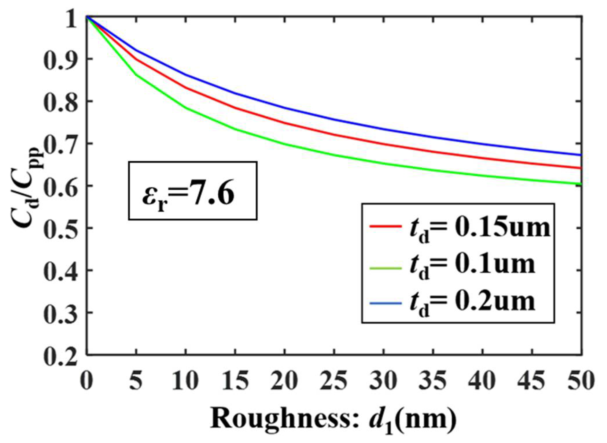
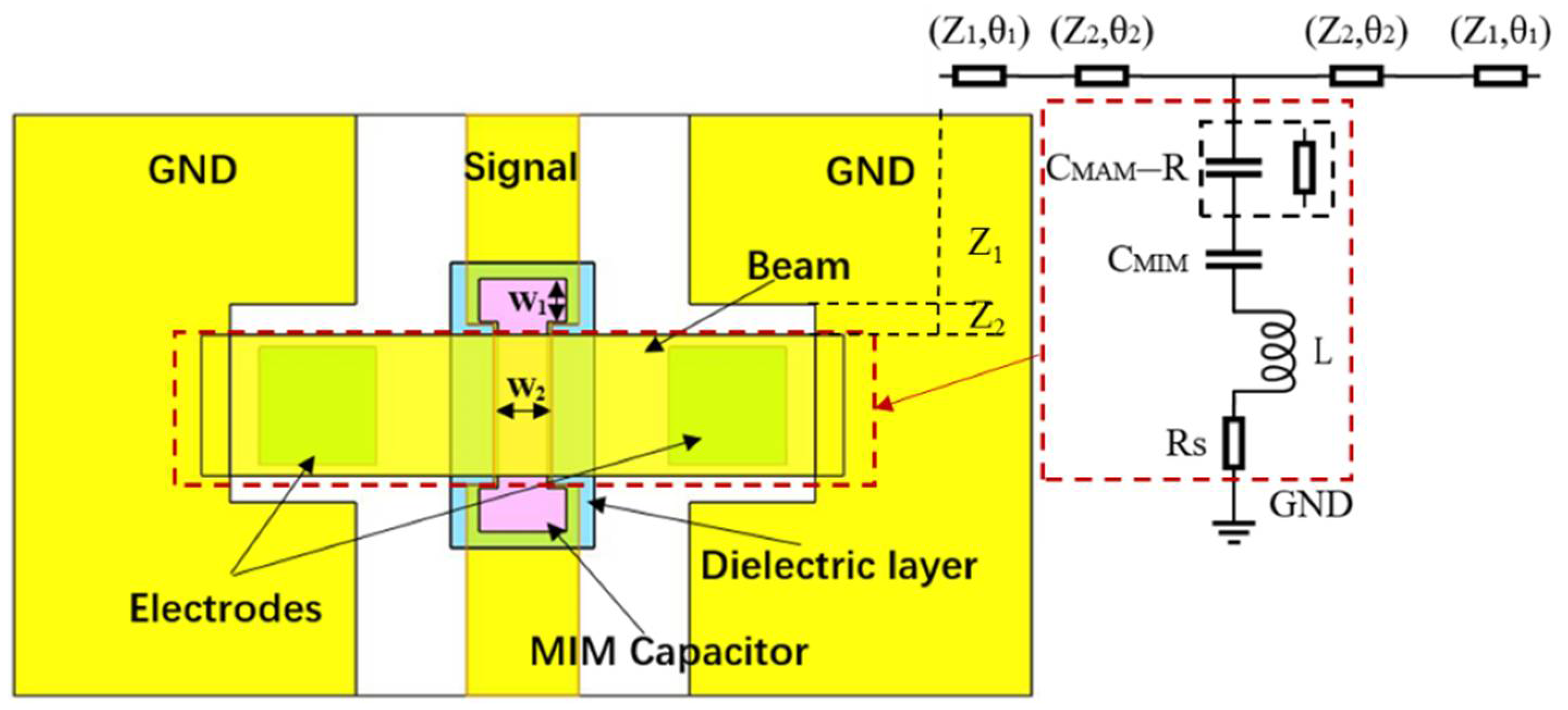
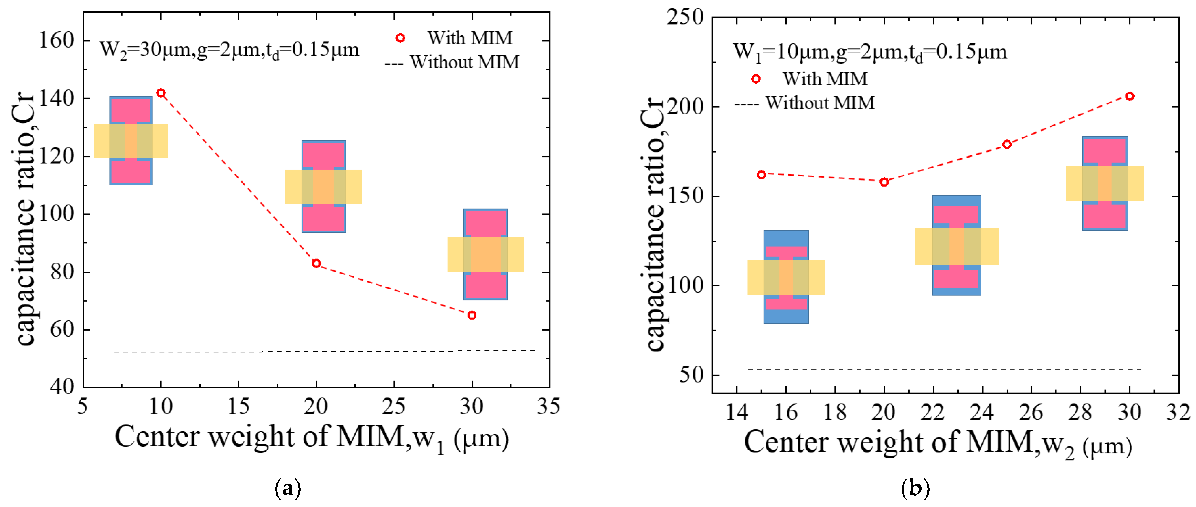
2.1. Metal-Insulator-Metal (MIM) Fixed Capacitor Design to Improve Switch Capacitance Ratios
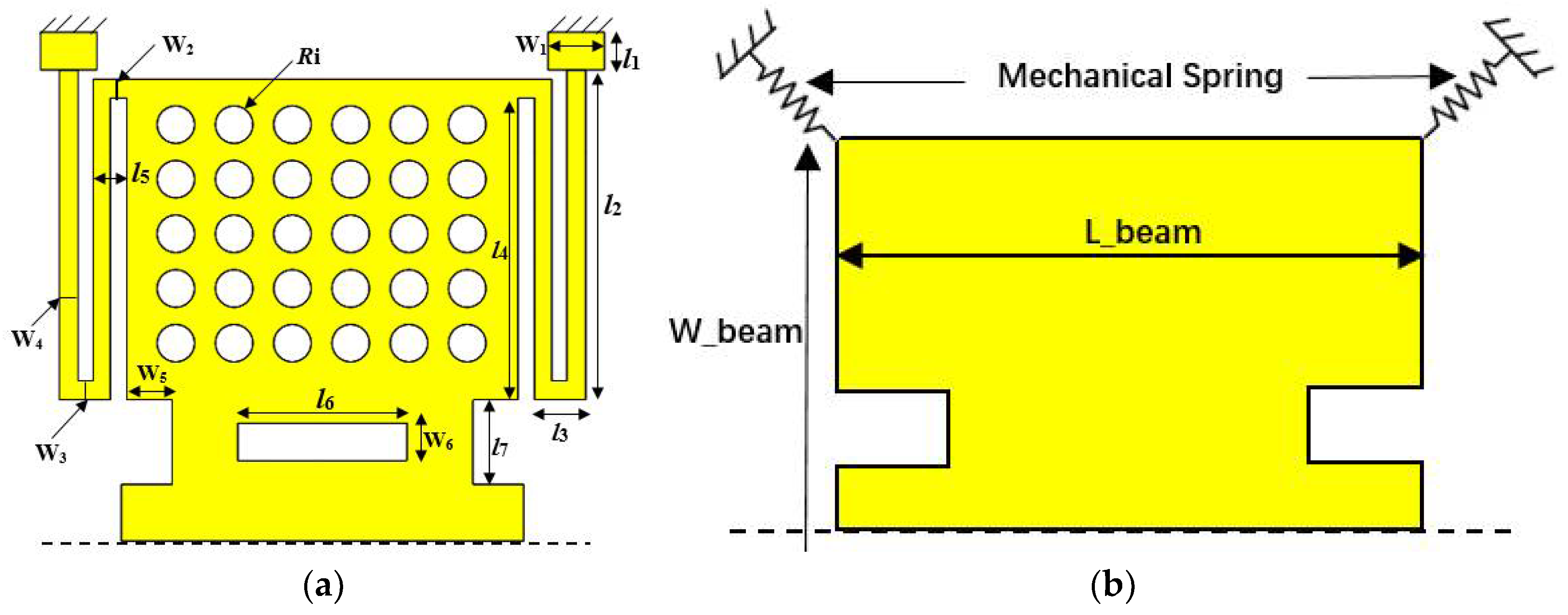
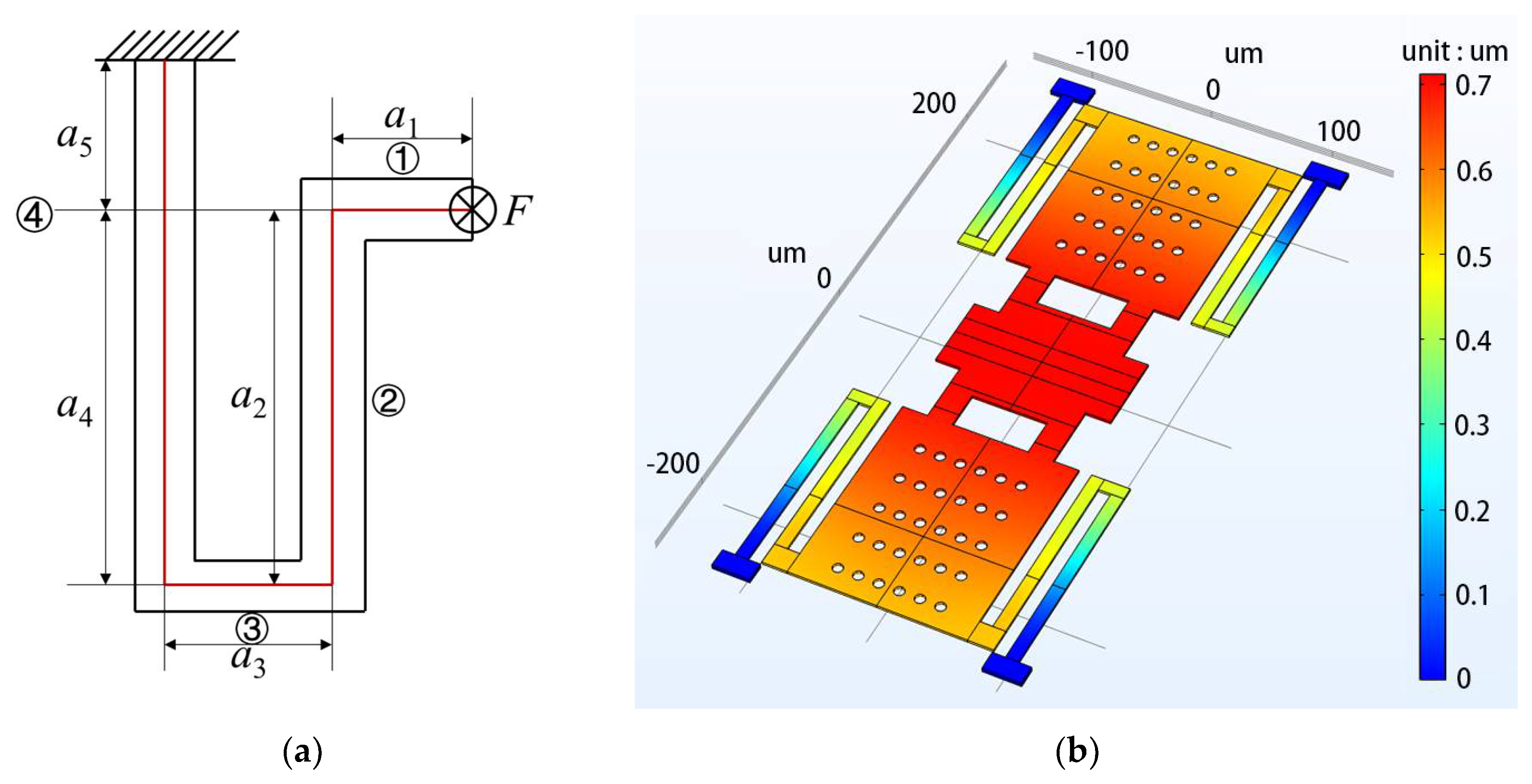
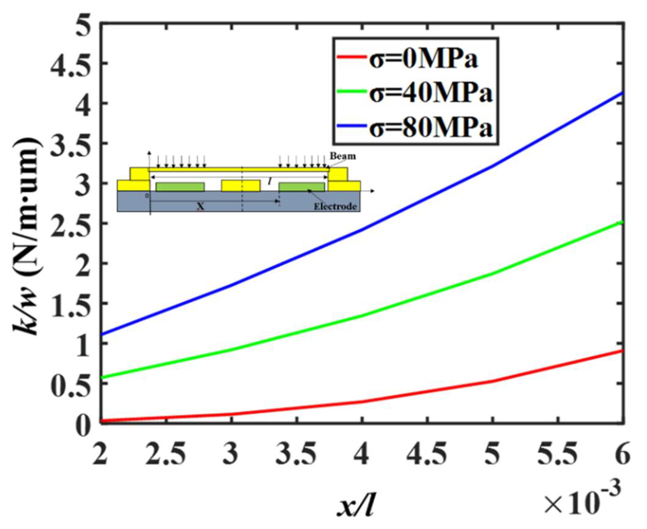
2.2. Low Spring Constant Bending Folding Beam Switch Design and Pull-Down Model
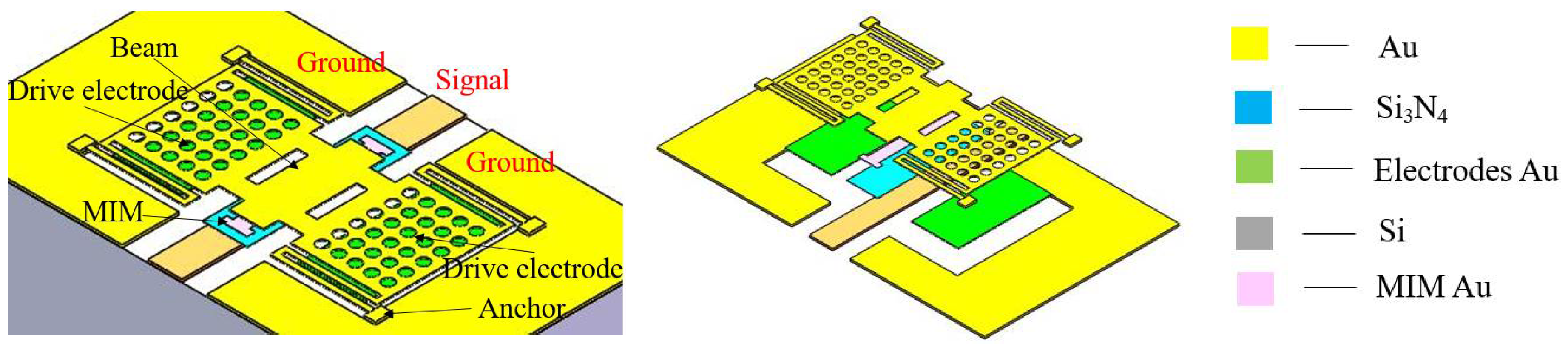
3. Physical Dimensions of the Proposed Switch
4. Discussion
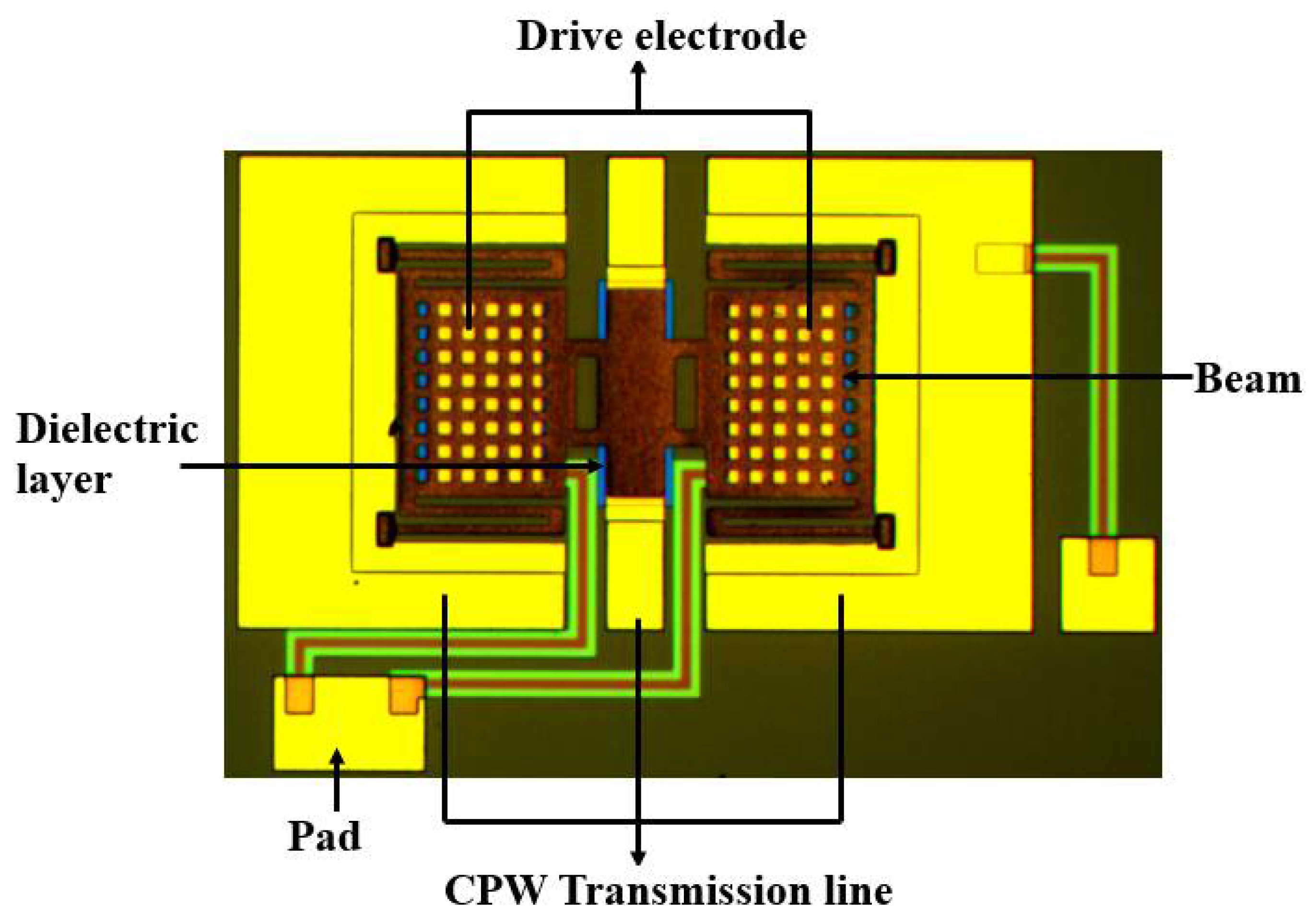
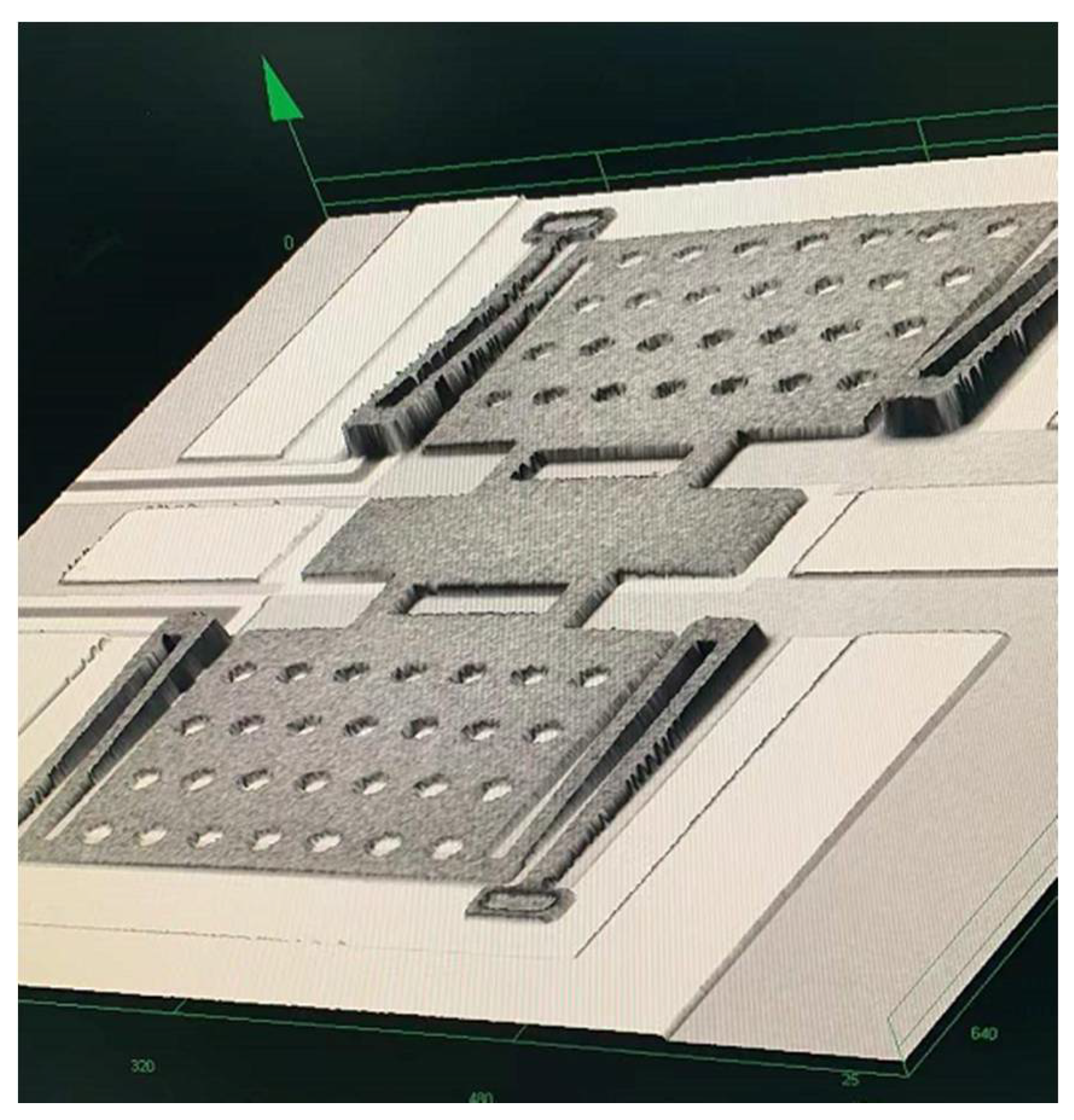
4.1. Fabrication
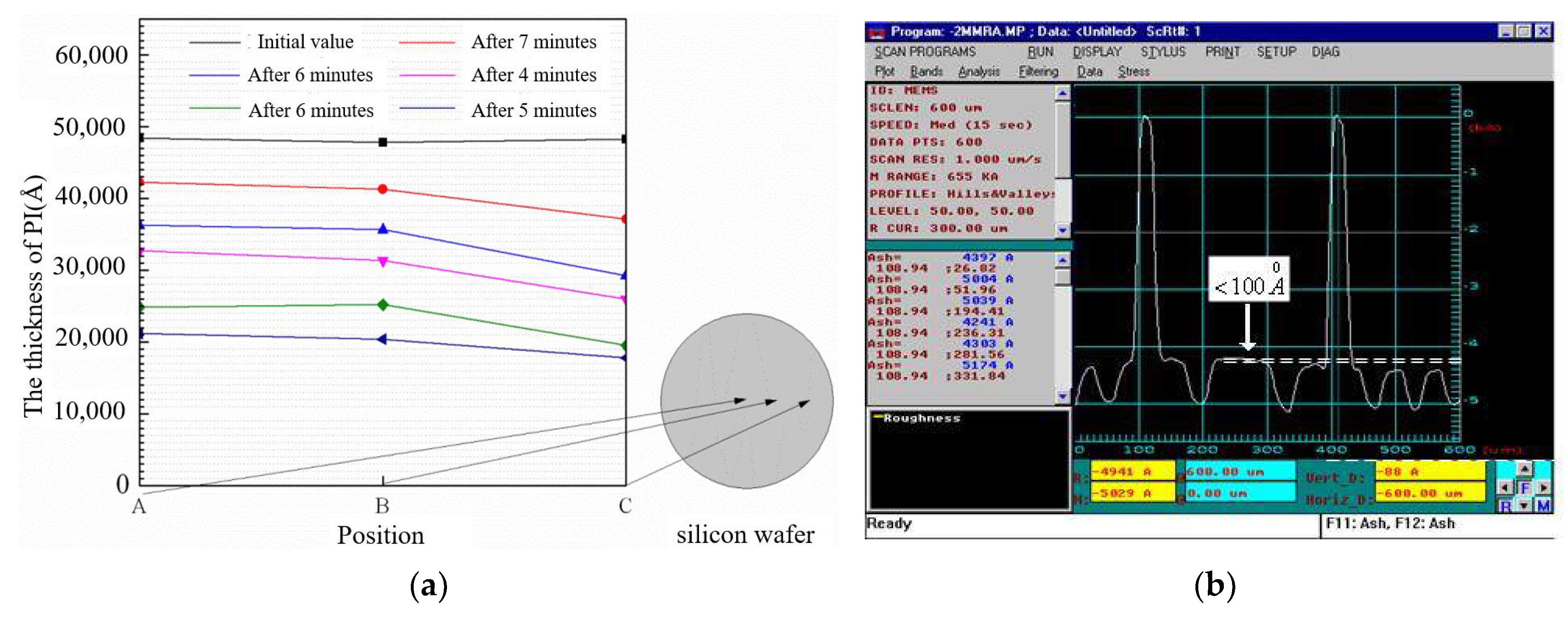
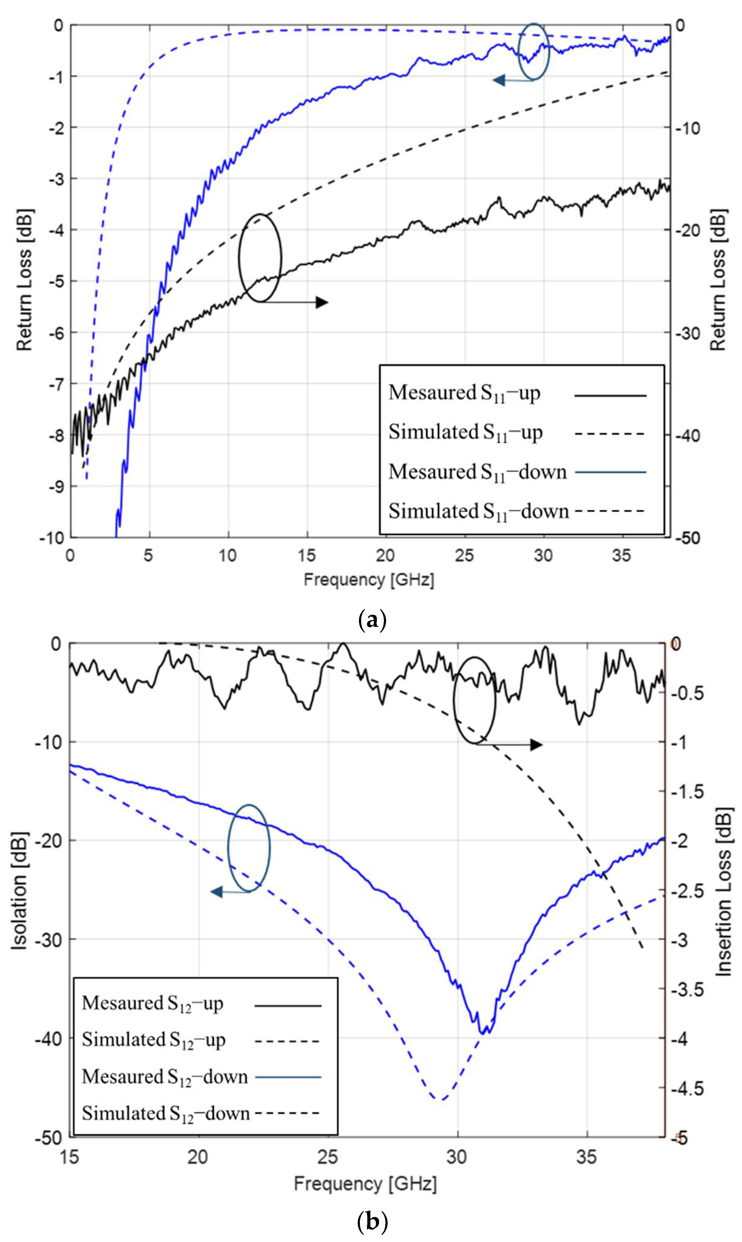
4.2. Measurement and Analysis
5. Conclusions
Author Contributions
Funding
Institutional Review Board Statement
Informed Consent Statement
Conflicts of Interest
References
- Kale, N.S. Tutorial T4: MEMS: Design, Fabrication, and their applications as chemical and biosenors. In Proceedings of the 28th International Conference on VLSI Design, Bangalore, India, 3–7 January 2015. [Google Scholar]
- Mansour, R.R. RF MEMS-CMOS Device Integration: An Overview of the Potential for RF Researchers. IEEE Microw. Mag. 2013, 14, 39–56. [Google Scholar] [CrossRef]
- Khushbu, M.; Deepak, B. Improved isolation RF MEMS switch with post release ashing. Microsyst. Technol. 2018, 24, 3863–3886. [Google Scholar] [CrossRef]
- Cohn, M.B.; Saechao, K.; Whitlock, M.; Brenman, D.; Tang, W.T.; Proie, R.M. RF MEMS switches for Wide I/O data bus applications. In Proceedings of the 2013 IEEE International Test Conference (ITC), Anaheim, CA, USA, 6–13 September 2013. [Google Scholar]
- Ko, C.H.; Ho, K.M.; Rebeiz, G.M. An Electronically-Scanned 1.8–2.1 GHz Base-Station Antenna Using Packaged High-Reliability RF MEMS Phase Shifters. IEEE Trans. Microw. Theory Tech. 2013, 61, 979–985. [Google Scholar] [CrossRef]
- Bozler, C.; Drangmeister, R. MEMs microswitch arrays for reconfigurable distributed microwave components. In Proceedings of the IEEE Antennas and Propagation Society International Symposium, Salt Lake City, UT, USA, 1–21 July 2000; pp. 587–591. [Google Scholar]
- Fouladi, S.; Mansour, R.R. Capacitive RF MEMS Switches Fabricated in Standard 0.35-CMOS Technology. IEEE Trans. Microw. Theory Tech. 2010, 58, 478–486. [Google Scholar] [CrossRef]
- Al-Dahleh, R.; Mansour, R.R. High-Capacitance-Ratio Warped-Beam Capacitive MEMS Switch Designs. J. Microelectromech. Syst. 2010, 19, 538–547. [Google Scholar] [CrossRef]
- Angira, M.; Sundaram, G.M.; Rangra, K.; Bansal, D.; Kaur, M. On the investigation of an interdigitated, high capcacitance ratio shunt RF-MEMS switch for X-band applications. Proc. NSTI Nanotechnol. 2013, 2, 189–192. [Google Scholar]
- Park, J.Y.; Kim, G.H.; Chung, K.W.; Bu, J.U. Fully intergrated micromachined capacitve switches for RF applications. In Proceedings of the 2000 IEEE MTT-S International Microwave Symposium Digest (Cat. No. 00CH37017), Boston, MA, USA, 11–16 June 2000; pp. 283–286. [Google Scholar]
- Park, J.Y.; Kim, G.H.; Chung, K.W.; Bu, J.U. Monolithically integrated micromachined RF-MEMS capcacitive switches. Sens. Actuators 2001, 89, 88–94. [Google Scholar] [CrossRef]
- Persano, A.; Quaranta, F.; Cola, A.; Taurino, A.; De Angelis, G.; Marcelli, R.; Siciliano, P. Ta2O5 thin films for capacitive RF-MEMS switched. J. Sens. 2010, 2010, 487061. [Google Scholar] [CrossRef] [Green Version]
- Ya, M.L.; Nordin, A.N.; Soin, N. Design and analysis of a low voltage electrostatic actuated RF CMOS-MEMS switch. In Proceedings of the RSM 2013 IEEE Regional Symposium on Micro and Nanoelectronics, Daerah Langkawi, Malaysia, 25–27 September 2013; pp. 41–44. [Google Scholar]
- Yongqing, X.; Ying, T.; Binzhen, Z.; Junping, D.; Li, Y. A novel RF MEMS switch on frequency reconfigurable antenna application. Microsyst. Technol. 2018, 24, 3833–3841. [Google Scholar]
- Li-Ya, M.; Anis, N.N.; Norhayati, S. Design, optimization and simulation of a low-voltage shunt capactive RF-MEMS switch. Microsyst. Technol. 2016, 22, 537–549. [Google Scholar]
- Deng, K.; Yang, F.; Deng, Z.; Wang, X.; Han, K. Analysis and design of a novel high capacitance ratio and low actuation voltage RF MEMS switch. Microsyst. Technol. 2021, 27, 1–11. [Google Scholar] [CrossRef]
- Rebeiz, G.M. RF MEMS: Theory, Design, and Technology; Wiley: New York, NY, USA, 2004. [Google Scholar]
- Entesari, K.; Rebeiz, G.M. A differential 4-bit 6.5-10-GHz RF MEMS tunable filter. IEEE Trans. Microw. Theory Tech. 2005, 53, 1103–1110. [Google Scholar] [CrossRef]
- Pozar, D.M. Microwave Engineering; Wiley: New York, NY, USA, 2009. [Google Scholar]
- Persano, A.; Cola, A.; De Angelis, G.; Taurino, A.; Siciliano, P.; Quaranta, F. Capacitive RF MEMS Switches with Tantalum-Based Materials. J. Microelectromech. Syst. 2011, 20, 365–370. [Google Scholar] [CrossRef]
- Badia, M.F.; Buitrago, E.; Ionescu, A.M. RF MEMS Shunt Capacitive Switches Using AlN Compared to Si3N4 Dielectric. J. Microelectromech. Syst. 2012, 21, 1129–1240. [Google Scholar] [CrossRef]
- Fall, M.; Fouladi, S.; Domingue, F.; Dieppedale, C.; Reig, B.; Mansour, R.R. High capacitance ratio RF MEMS dielectric-less switched capacitor. In Proceedings of the 2013 European Microwave Conference, Nuremberg, Germany, 6–8 October 2013; pp. 1327–1330. [Google Scholar]
- Bansal, D.; Kumar, A.; Sharma, A.; Kumar, P.; Rangra, K.J. Design of novel compact anti-stiction and low insertion loss RF MEMS switch. Microsyst. Technol. 2014, 20, 337–340. [Google Scholar] [CrossRef]
- Han, K.; Guo, X.; Smith, S.; Deng, Z.; Li, W. Novel High-Capacitance-Ratio MEMS Swich: Design, Analysis and Performance Verification. Micromachines 2018, 9, 390. [Google Scholar] [CrossRef] [Green Version]
- Liu, Y.; Taylor, T.R.; Speck, J.S.; York, R.A. High-isolation BST-MEMS switches. In Proceedings of the 2002 IEEE MTT-S International Microwave Symposium Digest (Cat. No. 02CH37278), Seattle, WA, USA, 2–7 June 2002. [Google Scholar]
- Yu, A.B.; Liu, A.Q.; Zhang, Q.X.; Alphones, A.; Zhu, L.; Shacklock, A.P. Improvement of isolation for MEMS capacitive switch via membrane planarization. Sens. Actuators A Phys. 2005, 119, 206–213. [Google Scholar] [CrossRef]
- Ziaei, A.; Dean, T.; Mancuso, Y. Lifetime characterization of capacitive RF MEMS switches. In Proceedings of the 2001 IEEE MTT-S International Microwave Sympsoium Digest (Cat. No. 01CH37157), Phoenix, AZ, USA, 20–24 May 2001. [Google Scholar]
- Rottenberg, X.; Jansen, H.; Fiorini, P.; De Raedt, W.; Tilmans, H.A.C. Novel RF-MEMS capacitive switching structure. In Proceedings of the 2002 32nd European Microwave Conference, Milan, Italy, 23–26 September 2002. [Google Scholar]
- Rizk, J.; Tan, G.L.; Muldavin, J.B.; Rebeiz, G.M. High-isolation W-band MEMS switches. IEEE Microw. Wirel. Compon. Lett. 2001, 11, 10–12. [Google Scholar] [CrossRef]


| Part | M(x) | T(x) | Vε |
|---|---|---|---|
| ① | |||
| ② | |||
| ③ | |||
| ④ |
| Symbol | Description | Value |
|---|---|---|
| l1 | Length of the anchor | 15 μm |
| l2 | Length in the mechanical spring | 170 μm |
| l3 | Length in the mechanical spring | 30 μm |
| l4 | Length in the rectangular plate | 150 μm |
| l5 | Length in the mechanical spring | 20 μm |
| l6 | Length of the rectangular hole | 60 μm |
| l7 | Length in the rectangular plate | 50 μm |
| lbeam | Length of the beam | 500 μm |
| w1 | Width of the anchor | 30 μm |
| w2 | Width in the mechanical spring | 20 μm |
| w3 | Width in the mechanical spring | 10 μm |
| w4 | Width in the mechanical spring | 10 μm |
| w5 | Width in the rectangular plate | 70 μm |
| w6 | Width of the rectangular hole | 30 μm |
| w7 | Width in the MIM capacitor | 30 μm |
| w8 | Width in the MIM capacitor | 10 μm |
| wbeam | Width of the beam | 220 μm |
| N | Number of circular slots | 56 |
| Ri | Radius of circular slots | 4 μm |
| tbeam | Thickness of the beam | 1.6 μm |
| td | Thickness of the dielectric layer | 0.15 μm |
| tMIM | Thickness of the MIM capacitor | 1 μm |
| Se | Area of actuation electrodes | 100 × 150 μm2 |
| g | Air gap | 2 μm |
| εr | Relative permittivity of dielectric layer | 7.6 |
| Author | Cup (fF) | Cdown (pF) | Cr | Insertion Loss (dB) | Isolation (dB) | Actuation Voltage (V) |
|---|---|---|---|---|---|---|
| Persano, A. [20] | 70 | 1.32 | 18.8 | <0.8@30 GHz | 38@23 GHz | 15–20 |
| Park, J. [10] | 83 | 50 | 600 | 0.08 | 42@28 GHz | 8 |
| Badia, M.F. [21] | - | 1.27 | - | 0.68@40 GHz | 35.8@40 GHz | 23.6 |
| Fall, M. [22] | 4.8 | 0.16 | 33.3 | 0.3@20 GHz | <1.5@20 GHz | 38 |
| Deepak, B. [23] | - | - | - | <0.1@20 GHz | [email protected] GHz | 20 |
| Li-Ya, M. [15] | 140 | 7.31 | 52 | 5.65@40 GHz | 24.38@40 GHz | 3.04 |
| Xu, Y.Q. [14] | - | - | - | 0.1@30 GHz | 26@30 GHz | 14 |
| Ke, H. [24] | 54 | 20.8 | 385 | <0.5@40 GHz | 34@10 GHz | 21 |
| Fouladi [7] | 23 | 2.1 | 91 | 0.98@20 GHz | 17.9@20 GHz | 82 |
| Liu, Y. [25] | 40 | 7 | 175 | 1.51@40 GHz | >30@16–36 GHz | 35 |
| Yu, A. [26] | 34.4 | 1.3 | 38 | <0.4@DC−40 GHz | 27@40 GHz | - |
| Ziaei, A. [27] | - | - | 400 | 0.1@10 GHz | 38@10 GHz | 35–40 |
| Rottenberg [28] | 18 | 7.98 | 459 | 0.06@1–15 GHz | 25@15 GHz | - |
| Rizk, J. [29] | 10 | 0.27 | 27 | 0.25 | 20@80–110 GHz | 30 |
| This paper | 26.5 | 4.3 | 162 | <0.5@30 GHz | [email protected] GHz | 15.8 |
Publisher’s Note: MDPI stays neutral with regard to jurisdictional claims in published maps and institutional affiliations. |
© 2021 by the authors. Licensee MDPI, Basel, Switzerland. This article is an open access article distributed under the terms and conditions of the Creative Commons Attribution (CC BY) license (https://creativecommons.org/licenses/by/4.0/).
Share and Cite
Deng, K.; Yang, F.; Wang, Y.; Lai, C.; Han, K. Design and Fabrication of a Ka Band RF MEMS Switch with High Capacitance Ratio and Low Actuation Voltage. Micromachines 2022, 13, 37. https://doi.org/10.3390/mi13010037
Deng K, Yang F, Wang Y, Lai C, Han K. Design and Fabrication of a Ka Band RF MEMS Switch with High Capacitance Ratio and Low Actuation Voltage. Micromachines. 2022; 13(1):37. https://doi.org/10.3390/mi13010037
Chicago/Turabian StyleDeng, Kun, Fuxing Yang, Yucheng Wang, Chengqi Lai, and Ke Han. 2022. "Design and Fabrication of a Ka Band RF MEMS Switch with High Capacitance Ratio and Low Actuation Voltage" Micromachines 13, no. 1: 37. https://doi.org/10.3390/mi13010037