Reliability is one of the most important considerations in microprocessor design. In today’s microprocessors, approximately 60% of the on-chip area is occupied by the cache [
1]. SRAM is an important part of the cache; however, because of the active feedback in the cross-coupled inverter pair, it can easily appear as a single-event upset (SEU) [
2]. In particular, data errors are more likely to occur in the case of low voltages [
3]. However, reducing the operating voltage is a common method used by current processors to reduce power consumption; therefore, it is necessary to consider the reliability of SRAM in the cache.
ECC is a commonly used protection method for SEU in SRAM, and usually includes parity and Single-Error Correction–Double-Error Detection (SEC–DED) code schemes [
4,
5,
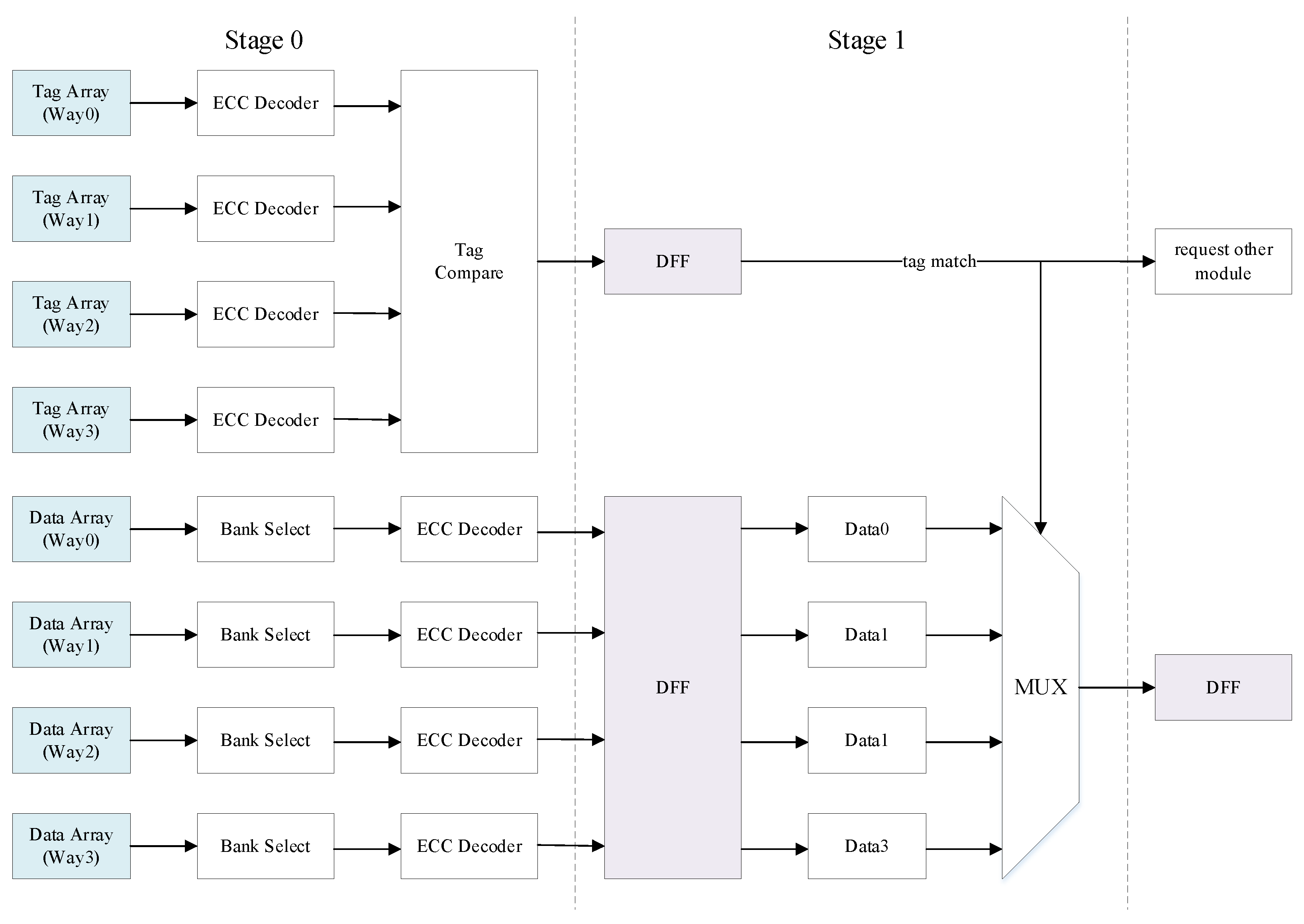
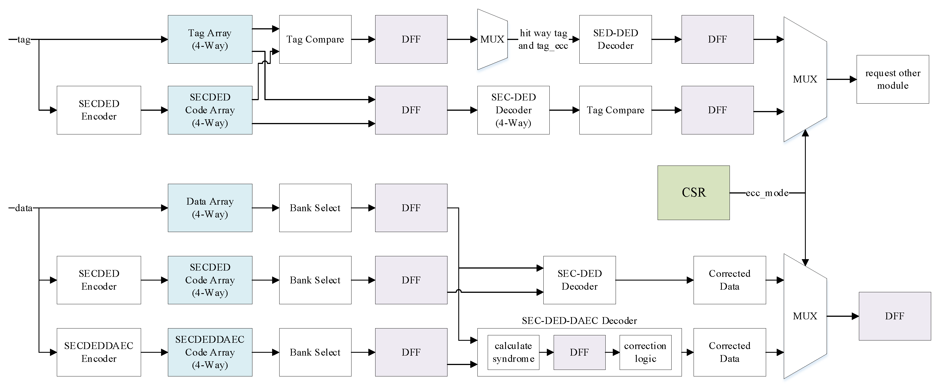
6]. SEC–DED is more widely used in cache because of its superior error correction and detection capabilities; however, SEC–DED also requires more complex encoding and decoding logic than parity, which increases circuit delay and easily limits the frequency of the cache. The cache needs tags and data to achieve its basic functions, and both tags and data are stored in SRAM. In the conventional ECC design scheme, after reading the tags and data from the SRAM, it directly passes through the ECC decoder, compares the corrected tag, and selects the corresponding data. The delay in this procedure is relatively large, which limits the frequency of the circuit. Compared with the conventional scheme using SEC–DED protection for both tags and data, this study proposes a high-performance pipeline design scheme with ECC in the cache, which uses SEC–DED to protect data but only detects errors of tags without correcting them. We use the TSMC 12 nm library for logic synthesis, and the results show that, after sacrificing a small part of the error correction ability, the theoretical maximum frequency of this data path increased from approximately 1.4 GHz in the conventional scheme to approximately 2.2 GHz, resulting in an approximate frequency increase of 57%. In addition, when the chip faces high-energy particles in the aerospace environment or the circuit enters low-voltage mode, it increases the possibility of SEU in the SRAM. Therefore, we also have higher reliability requirements in certain scenarios. With the scaling of process technology, the probability of multi-bit upsets (MBUs) is also increasing, and most MBUs occur in adjacent bits [
7]. Therefore, in addition to the above-mentioned high-performance circuit design scheme, this study also proposes a high-reliability circuit design scheme. In this scheme, SEC–DED is used to protect the tag and Single Error Correction–Double Error Detection–Double Adjacent Error Correction (SEC–DED–DAEC) proposed in [
8] is used to protect the data. The high-reliability mode improves error correction and can maintain the same frequency as the high-performance mode; however, the latency of accessing the cache increases by one cycle. There are different requirements for performance and reliability in different application scenarios. This solution supports switching between the above two modes by configuring an extended custom field in the control and status register (CSR), which improves the flexibility of the system.


