1. Introduction
Traditional contact cutting methods, such as a diamond saw blade, result in large kerf widths and debris generation with significant loss of material [
1,
2,
3]. Lasers are seen as a preferred tool to dice brittle materials as they are contactless. Lasers have been engaged in various sapphire wafer cutting techniques such as dual-wavelength double-pulsed laser irradiation [
4], laser-induced plasma-assisted ablation [
5,
6], controlled thermal cracking [
7], and filamentation [
8,
9]. Depending on the laser dicing technique, the surface roughness of sidewalls ranges from 50 nm to 2000 nm [
3].
Stealth dicing is a method that focuses the laser into a transparent material, for example glass or sapphire, minimizing the amount of top surface debris generated. For stealth dicing to work in an optically transparent material, an ultrashort pulse laser of sufficiently high intensity is necessary for nonlinear interaction and internal modification of the material. This will minimize the kerf width and debris produced [
3,
10,
11,
12].
In conventional stealth dicing methods, the laser light is focused into a single laser spot in the transparent sapphire sample [
10,
11,
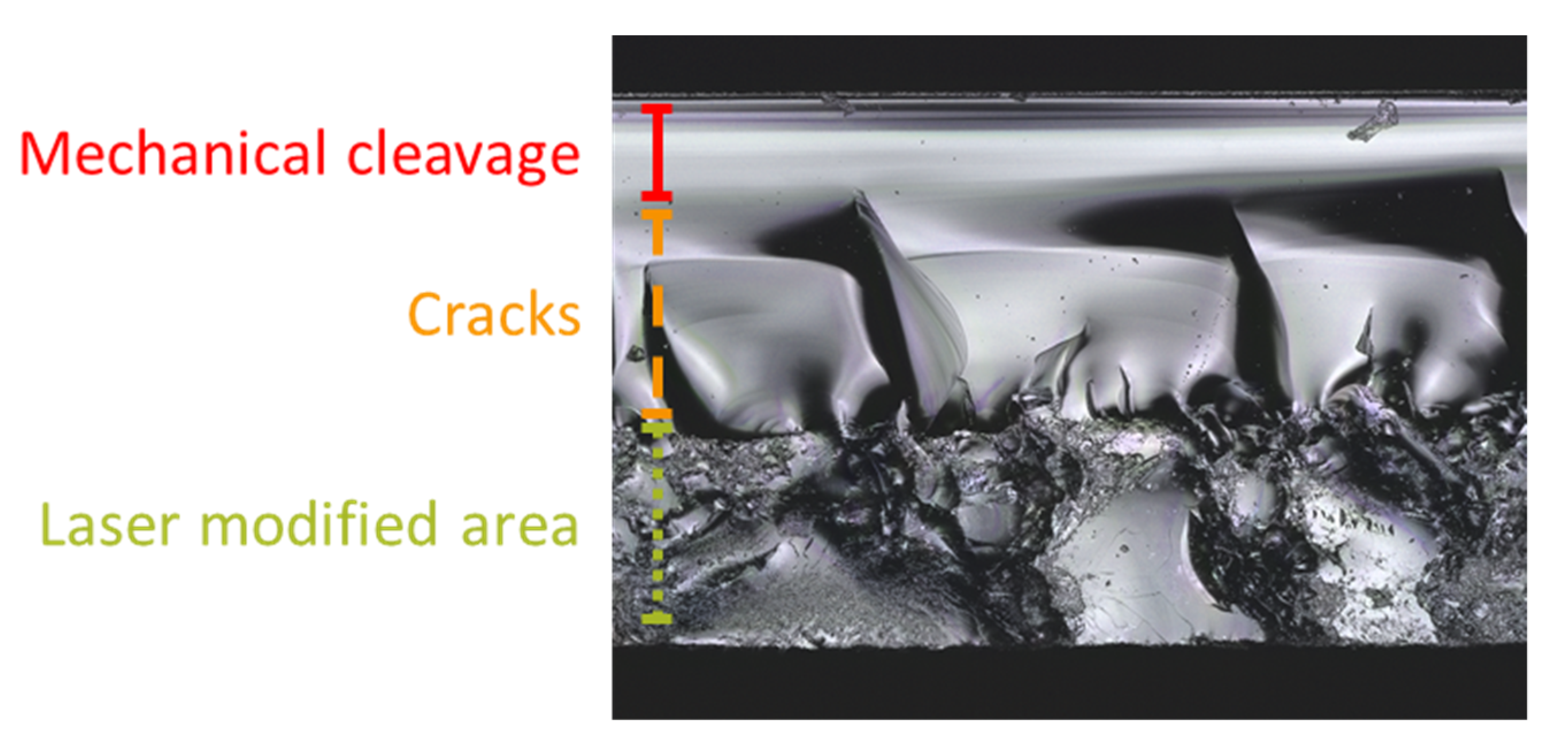
12]. These methods employ either single laser scan or multiple laser passes. With a single focus spot, there is an uneven distribution of laser energy within the samples, with rather non-uniform separation sidewall roughness. These sidewall profiles contain both rough laser-modified areas and smooth cleaved surfaces.
Multifocal optics has been employed with promising results to improve the stealth dicing of transparent materials. These include glasses and crystals of different thicknesses. Multi-foci laser irradiation distributes laser energy more evenly over the sample thickness with better controlled dicing. Current multi-foci laser dicing techniques generate multiple foci by employing concave mirrors [
13], annular coaxial focusing lenses [
14], and diffractive optical elements [
15,
16]. Allocating laser energy to multi-foci reduces the size of heat-affected zones and the extent of non-uniform distributions of thermal and mechanical stresses in the sample’s thickness, and hence reduces the possibility of crack formation [
13,
14,
15,
16]. These methods generally irradiate a transparent medium with a single laser scan only. It could be reasoned that introducing multi-foci for sample dicing could avoid the need for multiple laser passes.
However, if laser power is the limiting factor, integrating multi-foci laser scanning with multiple passes may be necessary. Ma et al. explored the use of Fresnel lenses, a type of diffractive optical element, to separate 2 mm thick sapphire wafers with four passes of multi-foci scanning over the entire thickness [
15]. A 1064 nm picosecond laser of 20 W power and 500 kHz repetitive rate was employed to irradiate the samples at 4 mm/s scanning speed. Four scans over four individual 0.5 mm sections were conducted with 15 foci. The laser pulse energy per focus may be calculated to be 2.67 μJ. Spherical aberration had been identified as a significant factor resulting in the reduction of laser energy density of the foci, especially for foci further from the laser source.
When compared with silicon and silicon carbide, sapphire is the most economically viable material as the main substrate in light-emitting diodes (LEDs) [
17]. Patterned sapphire substrates (PSS) were introduced to improve the performance of the conventional sapphire substrates [
18,
19,
20,
21]. The rough patterned surface of the PSS enhances the LED light extraction by increasing light scattering. The current method of etching the PSS structure into individual sapphire chips before growing the LED layers can be rather time consuming. Industrial-scale production can be expedited by first etching the patterns onto the wafers before singulation. Laser singulation of PSS can be challenging because of the apparent roughened surface. Light emission of LEDs grown on sapphire substrates can be further improved by introducing a roughened sidewall (i.e., the cleavage plane) [
11,
12,
21,
22]. It reduces internal reflection within the material. This enables a greater number of photons to escape from the material, which results in an increase in light extraction efficiency in LEDs. However, with non-uniformity in the sidewall profile by a single focus laser scan, the full potential of light emission in LEDs might not be realized [
10,
11,
12].
Our previous studies determined that for laser processing, a sapphire sample with a polished single surface was a better choice than one with both surfaces polished [
16,
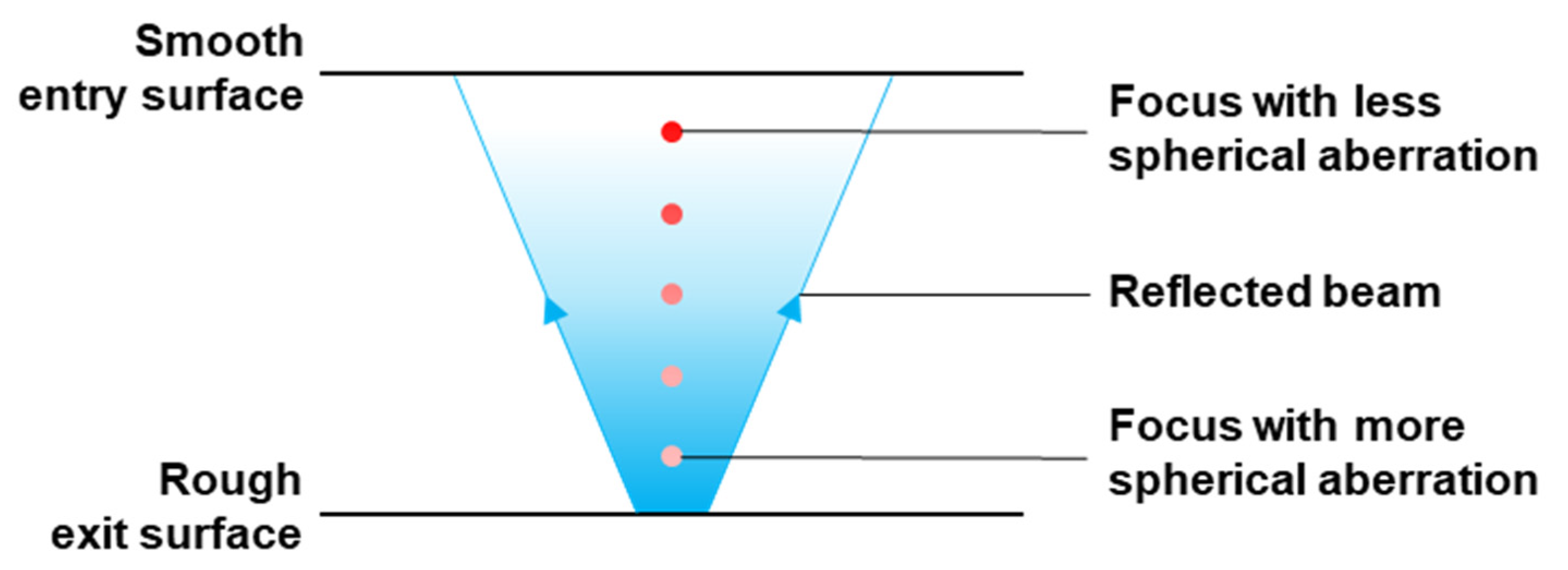
23]. The orientation of the roughened sample, either a laser entry or exit surface, has a significant effect on laser processing of the material. We have determined previously that some of the energy of the high-intensity laser beam is reflected back into the material by internal reflection at the rough exit surface. This partial internal reflection would be diffuse as the micro-surfaces of the rough surface are irregular. This reflected energy is trapped within the sample’s interior and decreases the transmission of light out of the sample. As a result, a significant amount of energy is accumulated within the sample to enhance nonlinear absorption. Nonlinear modification by a sample can facilitate the weakening of the sample sufficiently for its separation. Hence, this partial internal reflection phenomenon at the rough exit surface may be exploited for machining single-surface-polished sapphire samples.
Through multi-foci laser cutting technology for sapphire singulation, we have previously demonstrated that a roughened sidewall profile can be achieved through nonlinear modification at the various focus locations [
16]. Sample separation was achieved with the multi-foci laser focused over a single one-third section of the sample thickness. As such, only a portion of the thickness was nonlinearly modified to form a roughened sidewall. This large energy concentration at a single limited section instead of the overall thickness resulted in undesirable large wave-like cracks at the cleavage plane. With the multi-foci laser focused over the whole cross-section of the sample thickness, the roughened sidewall after sample cleavage remained rather non-uniform. Thus, the process requires improvement to achieve the desirable outcome of a uniformly roughened sidewall over the whole thickness of the sample after cleavage.
It is hypothesized here that by exploiting the partial internal reflection of a rough exit surface, the section next to the exit surface need not be scanned to achieve sample cleavage. In addition, as the exit section is furthest away from the laser source, focus next to the exit surface has the most severe spherical aberration [
15]. Thus, this approach may have the added benefit of alleviating the deteriorating effect of spherical aberration as laser beam reflection will reinforce its intensity. This hypothesis is verified in this investigation through two-zone partial thickness scanning. Two-zone partial thickness scanning is defined here as the multi-foci laser irradiation with two consecutive scans without scanning the full sample cross-section; each scan is directed at a different section of the sample’s thickness in the same scanning line. It is demonstrated that the desired outcomes can be achieved with effectivity and efficiency improvement of the singulation process by reducing the pulse energy per focus and amount of laser energy deposition required. By studying vastly different scanning speeds over a few orders of magnitudes, the pulse energies required for the desired sample cleavage and sidewall profiles can be estimated.
2. Materials and Methods
Single crystal
sapphire wafers of 50.8 mm in diameter and 0.43 mm in thickness were obtained from Latech Scientific Supply Pte. Ltd. (Singapore). The refractive index of the wafers was 1.768. The wafers were cut into 10 mm wide sample strips for easier handling. The wafers had their single polished surface oriented as the top laser entry surface [
23].
A stylus profilometer Form Talysurf Series 2 by Taylor Hobson was employed for surface roughness measurements. To measure the roughness of the sample surfaces (i.e., rough and smooth), the stylus travelled 10 mm across the center of the wafers. The measurements were conducted in two directions (i.e., 0° and 90°); each direction recorded 6 values for a total of 12 values. The averaged measurements in each direction for each sample surface were similar. The surface roughness for each sample surface was concluded to be uniform, without any orientation effect.
The polished surface roughness had Ra = 0.00193 μm (standard deviation 0.00015 μm) and Rz = 0.00980 μm (standard deviation 0.00061 μm). The rough surface roughness had Ra = 0.954 μm (standard deviation 0.059 μm) and Rz = 6.74 μm (standard deviation 0.544 μm). The rough surface roughness was similar to the PSS etching depth (i.e., from 0.4 μm to 1.5 μm) [
18,
19,
20]. Therefore, the roughened surface of the sapphire samples may be used as a proxy for a PSS surface.
For scanning a sample in its c-plane crystal orientation, a 10.3 ps laser by Time-Bandwidth Products AG (Zurich, Switzerland) was used. With a beam expander, the 1064 nm wavelength laser with vertical linear polarization had a 6.5 mm beam diameter, with an M2 value of 1.3. For high peak power and laser intensity, 50 kHz pulse repetition rate was used for a maximum laser power output of 2.4 W. The c-plane crystal-oriented sapphire sample was placed on an automated stage that controlled the laser scanning speed. The sample was scanned perpendicular to the laser’s optical axis.
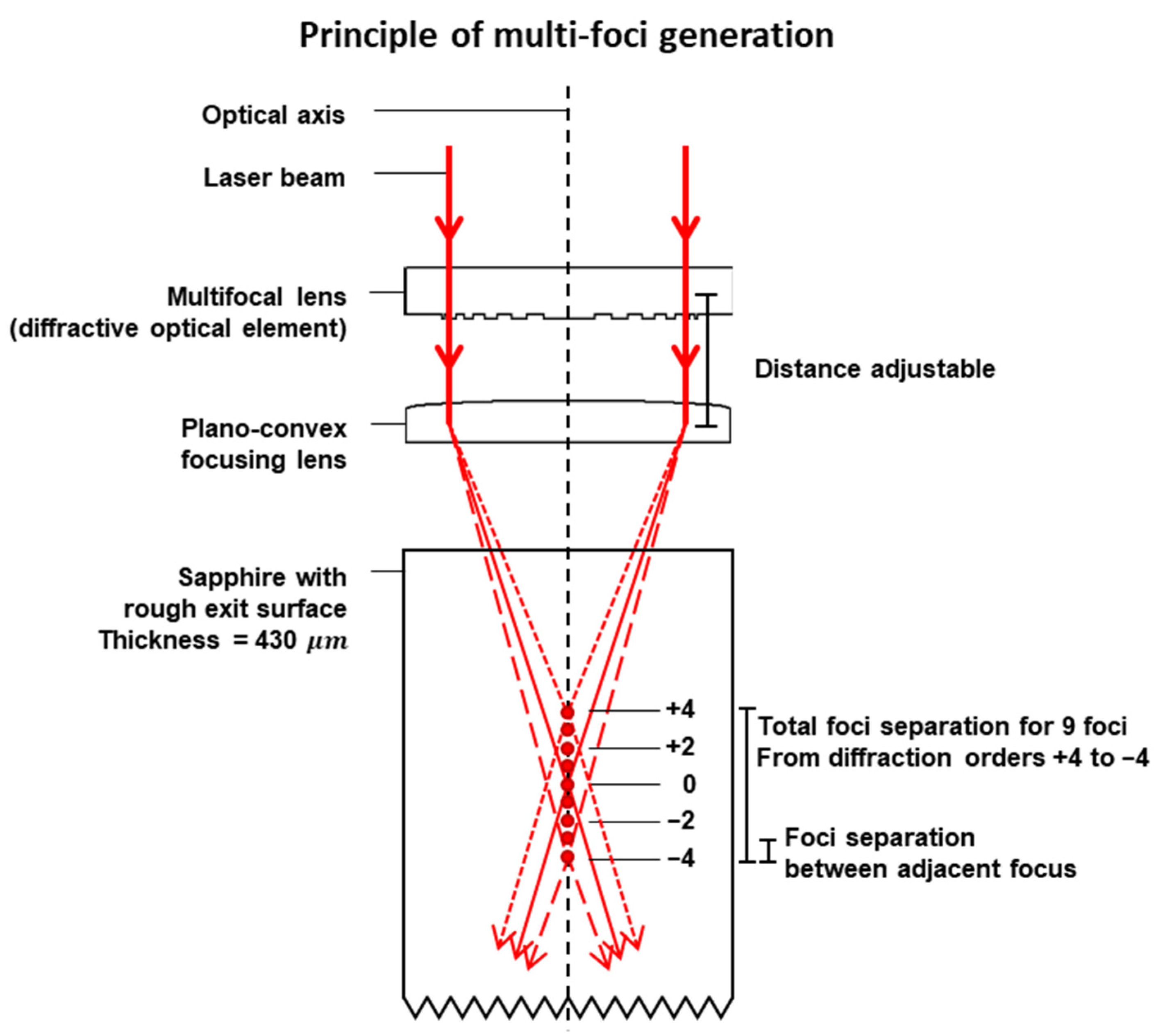
Two-zone experiments were conducted with a 9 foci multifocal lens (MF lens) and a plano-convex focusing lens with a 7.5 mm effective focal length (EFL). The MF lens is a form of diffractive optical element and the multifocal optics working principle has been previously discussed in [
16]. In summary, the MF lens diffracts and changes the phase angle of the incoming laser beam. The laser beam is then focused by the focusing lens to the various foci within the sapphire sample; see
Figure 1. The z position was calibrated first with only the plano-convex focusing lens (i.e., without the MF lens) to locate the focal plane of the laser beam. The focal plane of the focusing lens corresponded to the diffraction order 0 in the multi-foci setup. Subsequently, the MF lens was inserted to generate the multi-foci.
To facilitate discussion, the focused spot diameter with or without the MF lens may be assumed to be similar. As such, the focused spot diameter can then be calculated as 2.20 μm at the focal length. Our private communication with the manufacturer indicated that “
the light beams will mostly be the same, but not exact” [
24]. This indicates that although the focused spot diameter may not be exactly the same, it will be similar for all foci. By assuming similar focused spot diameter for all foci, the power density of each focus can be calculated approximately to be 1.65 MW/cm
2.
This experimental setup had a total foci separation of 136.3 μm, i.e., approximately one-third of the sample thickness (430 μm). Total foci separation is defined as the distance between the first and last foci generated, i.e., the distance between foci of diffraction orders +4 and −4 of this setup. The separation of the foci will differ in sapphire from that in air. This difference has been accounted for through calculations using the equations provided by the manufacturer [
24]:
where
is the focal length of diffraction order
,
is the focal length of refractive (focusing) lens,
is the focal length of diffractive (multifocal) lens, and
is the focal length of diffraction order
in a medium of refractive index
. Focal length values are absolute values measured from the principal plane of the focusing lens. When
,
.
For two-zone scanning, two out of the three non-overlapping scanning zones, namely the upper, middle, and lower one-third sections of the thickness, may be selected. Our separate investigation indicated that it is preferable to scan the section further from the laser source first; this is then followed by a second scan on a section closer to the laser source. This ensures that nonlinear modifications, if any, from the first scan would not interfere undesirably with the second scan.
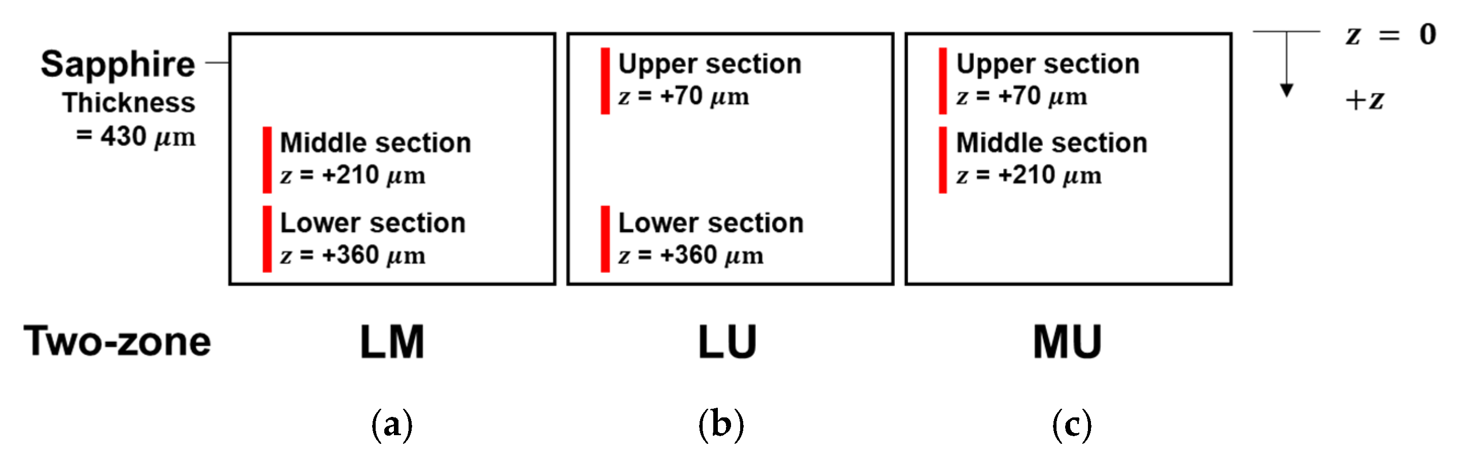
Each scanning zone was labeled with “L”, “M”, or “U” to indicate the lower, middle, or upper one-third section, respectively. Since two consecutive scans were conducted for each sample, the order of the labels indicated the order of the scans conducted. The different two-zone combinations were identified as LM, LU, and MU, respectively. For example, LM means that the lower section is scanned first, and then the middle section is scanned over the same scanning line.
Figure 2 shows the schematic of different two-zone combinations (i.e., LM, LU, and MU). Each vertical solid line signifies all the foci positions for each scanned section. The diffraction order 0 is the middle focus at the mid-point (i.e., at the
values shown) in the vertical column of multi-foci as indicated by the vertical line.
For all experiments, each one-third section was scanned by a 0.57 W laser beam which is approximately a quarter of the maximum laser power output. This is to demonstrate that a key practical limitation due to the laser power constraint could be effectively addressed by this proposed approach. The laser pulse energy per focus was calculated as 1.26 μJ, which was less than half of 2.67 μJ in [
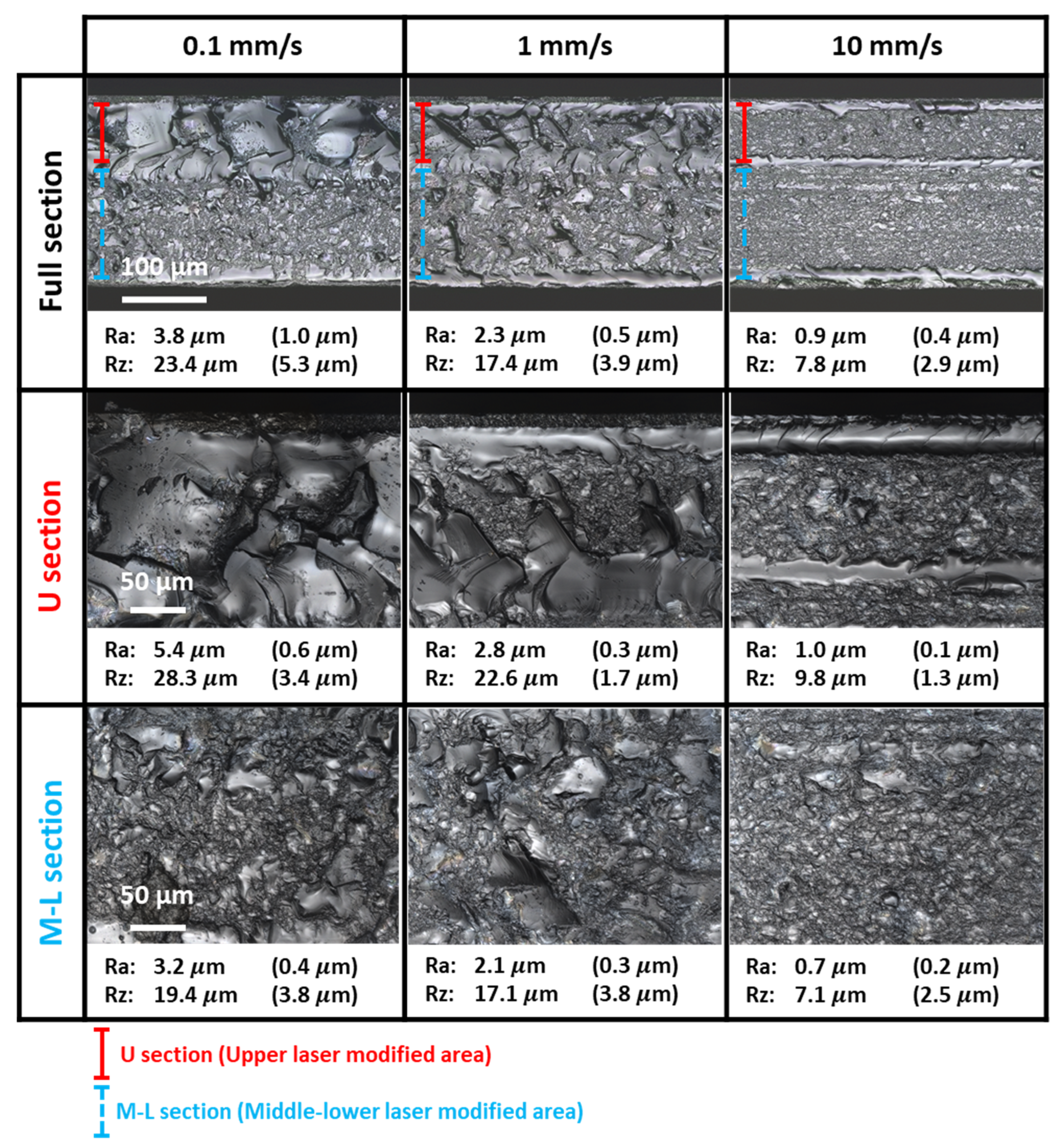
15]. The effects of energy deposition within a sample were studied with three scanning speeds, namely 0.1, 1.0, or 10 mm/s. These scanning speeds were chosen to increase by an order of magnitude to cover a large range of scanning speeds and hence pulse energies deposition into a sample. A slower scanning speed would result in more energy deposited; see
Table 1. This allows the estimation of the energies required to achieve sample separation with the desired sidewall profiles.
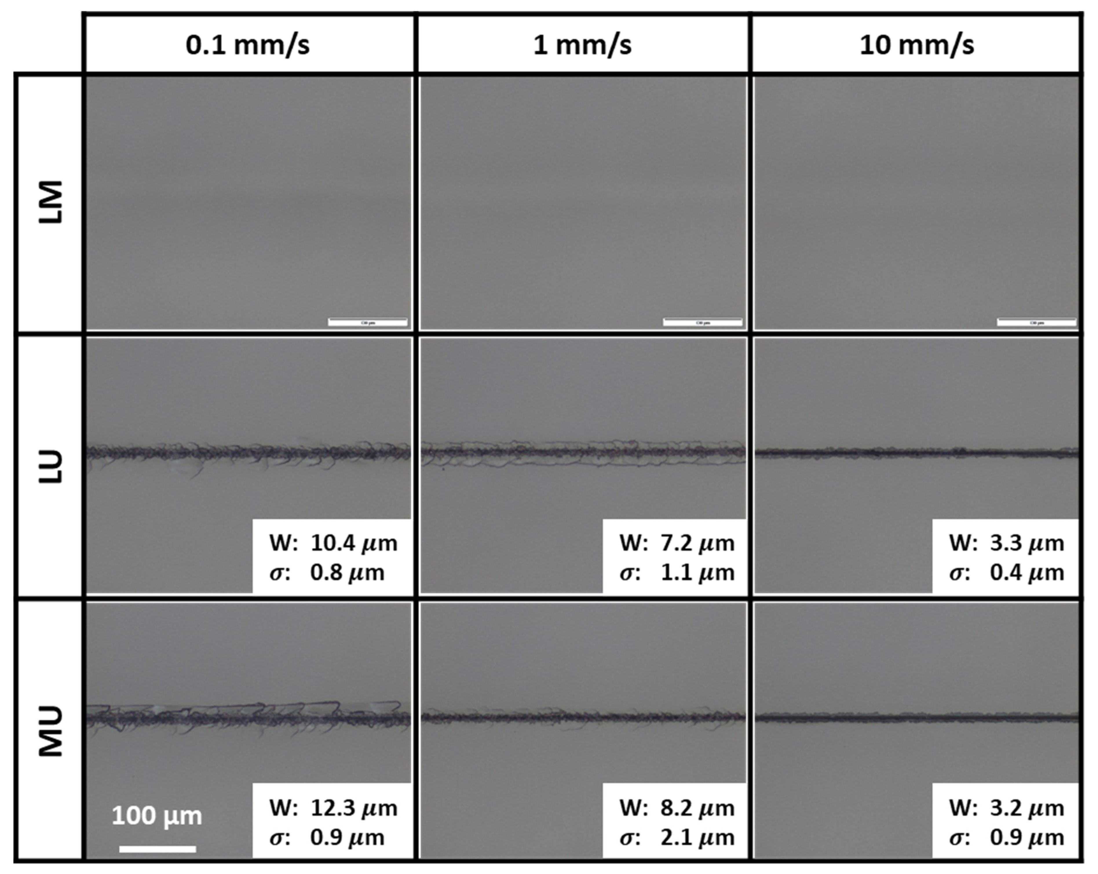
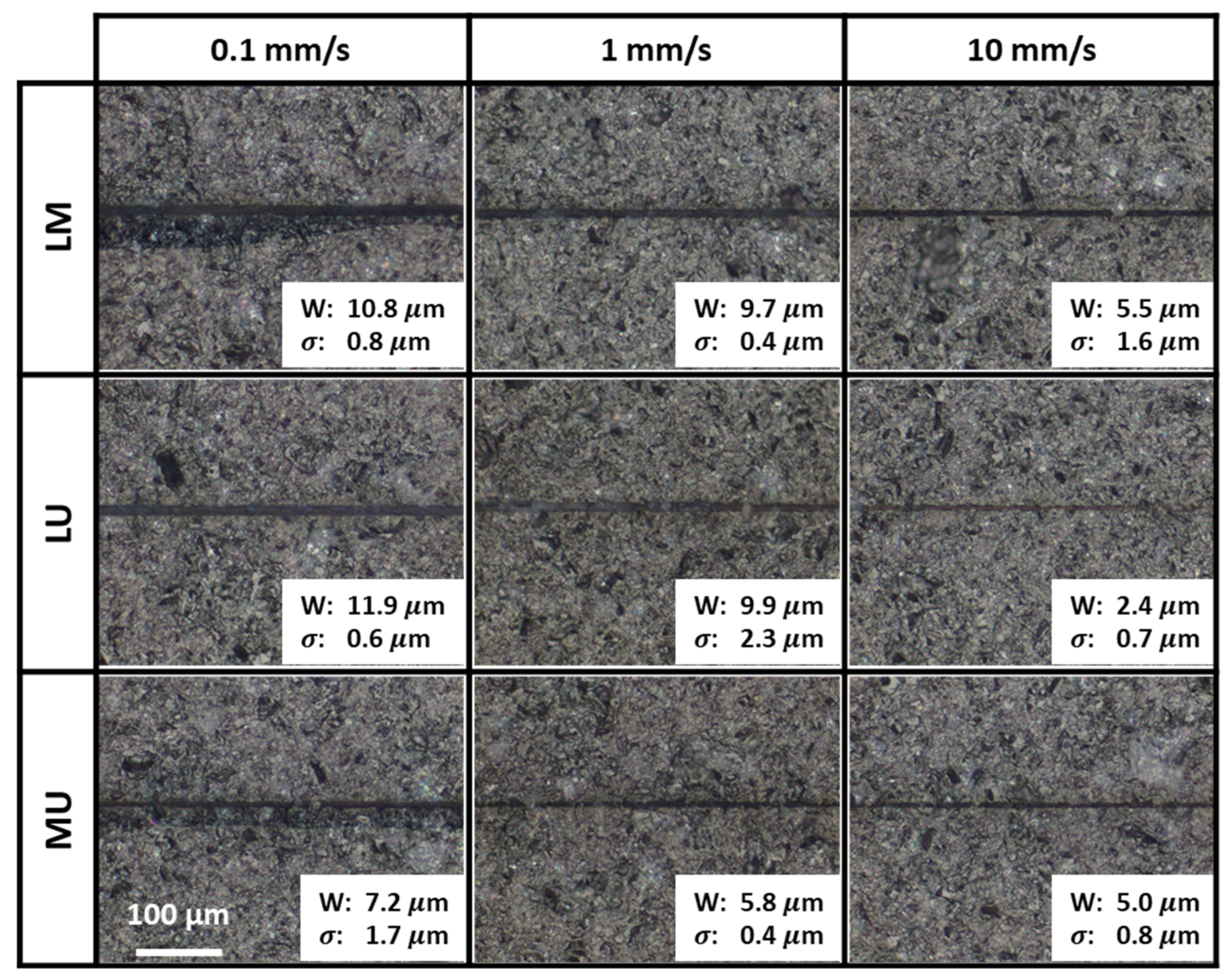
Through stealth dicing, the sample surface was rather clean. The samples were only cleaned with a gentle wipe by a lens cloth before examination under Olympus BX51 fluorescent microscope. After laser irradiation, the samples were mechanically cleaved. For samples that could be separated, they can be easily cleaved by hand with a normal force applied along the laser-scribed lines to aid the propagation of cracks for sample separation. If the samples failed to separate or the plane of separation deviated from the intended separation plane (i.e., laser-scribing plane), “no cleavage” was recorded for the sample. Indeed, for those samples that failed to separate, an increase in the normal force might result in large separation deviation from the intended separation plane, or the sample remained intact. The sidewall profiles of successfully cleaved samples were examined with a confocal laser scanning microscope VK-110 by Keyence.
4. Conclusions
Multi-foci laser cutting technology has been adapted for machining transparent sapphire wafers [
15,
16]. This investigation proposed an approach of employing two-zone partial thickness scanning for machining a single-surface polished sapphire sample. Cleavable samples were achieved with two-zone MU scanning. It scanned only the top two-third thickness by first scanning the middle section, then the upper section. The upper section scan resulted in nonlinear modifications in the upper section. The middle section scan formed nonlinear modifications in both the scanned middle and non-scanned lower sections. Despite this partial thickness scanning, the cleaved samples had a uniformly roughened sidewall profile over the entire thickness. This is a desirable outcome in LED manufacturing.
It should be noted that scanning either the upper one-third and lower one-third sections (i.e., two-zone LU) or the lower two-third sections of the sample thickness (i.e., two-zone LM) did not result in sample cleavage. By comparing MU, LU, and LM scanning, it is further hypothesized that the effect of beam reflection at the rough exit surface is significant. The beam reflection could well alleviate the focusing imperfection caused by spherical aberration. More importantly, there could be an increase in laser intensity at the non-scanned section in MU through partial internal reflection of the laser beam. It provides a plausible explanation that in MU scanning, the non-scanned one-third section next to the exit surface showed clear laser damage at the cleaved surface. However, we will not rule out that there could well be other possible explanations for our observations.
This technique of partial thickness two-zone MU scanning resulted in a cleavable sample with the desirable uniformly roughened sidewall profile. Quality outcomes were achieved with less energy usage and a faster scanning speed, and thus an improvement of laser energy effectivity and efficiency. Although double scans have been demonstrated in this investigation, it does indicate the possibility of increasing the number of scans and scanning sections for a thicker sample if necessary to achieve sample separation. The laser power utilized is approximately a quarter of the total power of the laser system. This provides much room to increase the laser power with more foci over a larger total foci separation distance for a thicker sample. This investigation can be further extended to other materials such as the laser singulation of single-surface polished silicon wafer with a rough surface as the exit surface. However, optimization of the various process parameters will be necessary for the specific applications as required.
In addition, for a better understanding of the exact mechanism, a thermal camera may be employed to quantitatively evaluate the interaction of the reflected laser beam on the multi-foci of the incoming beam at the various one-third sections. A comparison between the results of single-surface and double-surface polished samples could explain the effects of beam reflection and its effectiveness in reducing the problems caused by spherical aberration.


