Article

Process Control Monitor (PCM) for Simultaneous Determination of the Piezoelectric Coefficients d31 and d33 of AlN and AlScN Thin Films

1
State Key Laboratory of Transducer Technology, Shanghai Institute of Microsystem and Information Technology, Chinese Academy of Sciences, Shanghai 200050, China
2
School of Graduate Study, University of Chinese Academy of Sciences, Beijing 100049, China
3
Shanghai Industrial μTechnology Research Institute, Shanghai 201800, China
4
School of Microelectronics, Shanghai University, Shanghai 200444, China
*
Author to whom correspondence should be addressed.
Micromachines 2022, 13(4), 581; https://doi.org/10.3390/mi13040581
Submission received: 3 March 2022 / Revised: 2 April 2022 / Accepted: 5 April 2022 / Published: 7 April 2022

Abstract

:
Accurate and efficient measurements of the piezoelectric properties of AlN and AlScN films are very important for the design and simulation of micro-electro-mechanical system (MEMS) sensors and actuator devices. In this study, a process control monitor (PCM) structure compatible with the device manufacturing process is designed to achieve accurate determination of the piezoelectric coefficients of MEMS devices. Double-beam laser interferometry (DBLI) and laser Doppler vibrometry (LDV) measurements are applied and combined with finite element method (FEM) simulations, and values of the piezoelectric parameters d33 and d31 are simultaneously extracted. The accuracy of d31 is verified directly by using a cantilever structure, and the accuracy of d33 is verified by in situ synchrotron radiation X-ray diffraction; the comparisons confirm the viability of the results obtained by the novel combination of LDV, DBLI and FEM techniques in this study.

1. Introduction

Piezoelectric thin films are widely used in various microelectromechanical systems (MEMS), such as communication devices [1], applications in the automotive industry [2], medical devices [3], and other integrated sensors and actuators [4,5]. These devices and systems are rapidly prevailing in the market [6]. Aluminum nitride (AlN) thin films have gained significance as piezoelectric materials due to their complementary metal-oxide semiconductor (CMOS) compatibility [7], high-temperature, long-term stability, high voltage resistance and good electrical insulation properties [8,9]. Moreover, research has shown that a significant increase in the piezoelectric constants d33 and d31 can be achieved by doping transition metals into AlN, with scandium (Sc) being the foremost option [10]. The characteristic parameters of piezoelectric materials not only influence the performance of MEMS but also affect their electromechanical conversion efficiency. To precisely predict the electromechanical performance of MEMS devices, the use of finite element method (FEM) software for device design requires accurate implementation of the elastic, dielectric and piezoelectric properties [11]. Therefore, accurate and efficient measurement of the characteristic parameters of piezoelectric films is important. Research has shown that the performance of these sensors and actuators is mainly related to the transverse piezoelectric coefficient d31 and the longitudinal piezoelectric coefficient d33 and is less affected by other parameters of the piezoelectric coefficient matrix, such as d11, d12, d13, d14, d15, d16, d21, d22, d23, d24, d25, d26, d32, d34, d35, and d36 [1,2,3,4,5].
There are various measurement techniques for piezoelectric thin films, such as using the direct piezoelectric effect by measuring the resulting voltage upon application of mechanical stress or using the inverse piezoelectric effect by measuring voltage-induced mechanical expansion or compression.
The formulas of the inverse piezoelectric effect and the positive piezoelectric effect of the longitudinal piezoelectric coefficient d33 are:
d 33 = S 3 E 3 T
d 33 = D 3 T 3 E
The formulas of the inverse piezoelectric effect and the positive piezoelectric effect of the transverse piezoelectric coefficient d31 are:
d 31 = S 1 E 3 T
d 31 = D 3 T 1 E
where S is strain; E is electric field; D is electrical displacement; T is stress; 1 is x-axis direction; and 3 is z-axis direction.
Lefki and Dormans proposed the direct piezoelectric measurement method and studied the ideal situation suitable for substrate clamping and interactions between electrode and substrate sizes. They showed that d33 obtained by the direct measurement method is the effective value d33,f and affected by the clamping of the substrate. The relationship between d33 and d33,f is given by [12]:
d 33 , f = d 33 2 d 31 s 13 , p s 11 , p + s 12 , p
where d33 and d31 are the actual longitudinal and transverse piezoelectric coefficients, and s11,p, s12,p, and s13,p are the compliance coefficients of the piezoelectric film.
The method of using a MEMS structure to extract piezoelectric properties has been thoroughly studied. In general, only one piezoelectric parameter (d31 or d33) can be obtained by the method mentioned above. For example, d31 can be extracted by using cantilever bending, which requires a dedicated process for cantilever release [13]. Since the performance of a film bulk acoustic resonator (FBAR) device is mainly affected by d33, the performance of a surface acoustic wave (SAW) device is mainly affected by d31. After measurement of the electrical and acoustic characteristics of a film, the piezoelectric co-efficient can be calculated; therefore, it is possible to use SAW resonators to extract d31 or FBARs to extract d33 [8,9,10,11,12,13,14]. However, when using this approach, various input parameters—such as the dielectric constant or sound velocity—should be determined before performing the electroacoustic characterization of fabricated FBAR and SAW devices, which introduces further uncertainties in their equivalent electrical circuit model.
In addition, the longitudinal deformation of a film can be measured by laser interferometry to characterize its longitudinal piezoelectric coefficient d33. Since the displacement of a piezoelectric film is very small (from pm to nm), optical interferometry, such as laser Doppler vibrometry (LDV) or double-beam laser interferometry (DBLI), is used to characterize the piezoelectric constant of the film (related to d33) [15]. When a piezoelectric film was deposited on a silicon wafer and not carefully clamped, Kholkin et al. found a quadratic relationship between the displacement measurement and the length of the electrode. A small electrode and hard conductive adhesive were used to inhibit substrate bending and improve test accuracy [16,17].
In general, it is difficult to simultaneously extract the piezoelectric coefficients d31 and d33 using a single test structure. A MEMS sensor based on piezoelectric films mainly utilizes the positive piezoelectric effect of the film during operation and realizes the sensing function by applying out-of-plane stress (related to d33) and then detecting the corresponding polarized charge. The actuator mainly uses the inverse piezoelectric effect of the film to apply an electric field in the polarization direction of the film to generate mechanical deformation in the longitudinal direction (related to d33) or transverse direction (related to d31) to drive the actuator. The performance of piezoelectric thin-film-based MEMS devices is usually affected by d31 and d33. Therefore, to accurately predict device performance, it is necessary to input accurate values of d31 and d33 during simulation analysis.
Recently, Mayrhofer et al. reported a 2-port electrode design based on the finite element (FEM) method and used it to measure the piezoelectric constant of AlScN films [17,18]. This measurement proved that it was possible to simultaneously extract the piezoelectric coefficients d33 and d31. However, they adopted empirical values from other studies as input parameters for their FEM simulations, which resulted in a larger amount of computation. The accuracy of their results has not yet been verified by other methods.
In this paper, we report a fabrication process for PCM test structures that does not require process steps in addition to patterning the AlScN and Mo electrodes. Due to the simplicity of the manufacturing process, the PCMs are compatible with most piezoelectric MEMS device fabrication processes. One great advantage lies in the significance of accurately defining the material parameters of the device, since the growth conditions of a piezoelectric film have a very obvious effect on its performance, and films grown in different batches have large performance differences. The DBLI method is used to pretest the longitudinal piezoelectric coefficient d33. It provides an intermediate reference value for the piezoelectric parameter scan in the simulation, which reduces the calculation time, shortens the bivariate iteration cycle and improves the extraction efficiency of the piezoelectric coefficient. The following sections of this paper characterize the material parameters of the two piezoelectric films (AlN and Al0.8Sc0.2N) used for the tests in this study, discuss how the PCM test structure was fabricated using the MEMS process, and explain how FEM simulations were efficiently used to simultaneously characterize the longitudinal (d31) and transverse (d33) piezoelectric constants. We then describe how we observed the reversible elongation and contraction of lattice parameters in situ under applied electric fields using synchrotron X-ray diffraction. The effective longitudinal piezoelectric constant d33 was estimated from the relationship between the electric field and the field-induced strain, which verified the d33 result obtained by the LDV-FEM method. The results for d31 were verified with the coefficients characterized by the cantilever method.

2. Materials and Methods

2.1. Preparation

A straightforward, 4-mask microfabrication process was developed for the fabrication of the PCM. Figure 1 shows the process of preparing a PCM on a 4-inch wafer. The top electrode was patterned by ion beam etching (IBE), and the 1-μm AlScN piezoelectric layer was wet etched with dilute tetramethylammonium hydroxide (TMAH) [19]. Since Sc doping increased the chemical resistance of the aluminum nitride film, it was necessary to increase the etching time for AlScN compared to undoped AlN. The top and bottom electrodes were electrically isolated by a SiO2 dielectric layer, followed by the growth of a Ti/Au metal layer, which was then patterned with IBE to obtain the shape of the test electrode for the PCM.

2.2. Physical Analysis

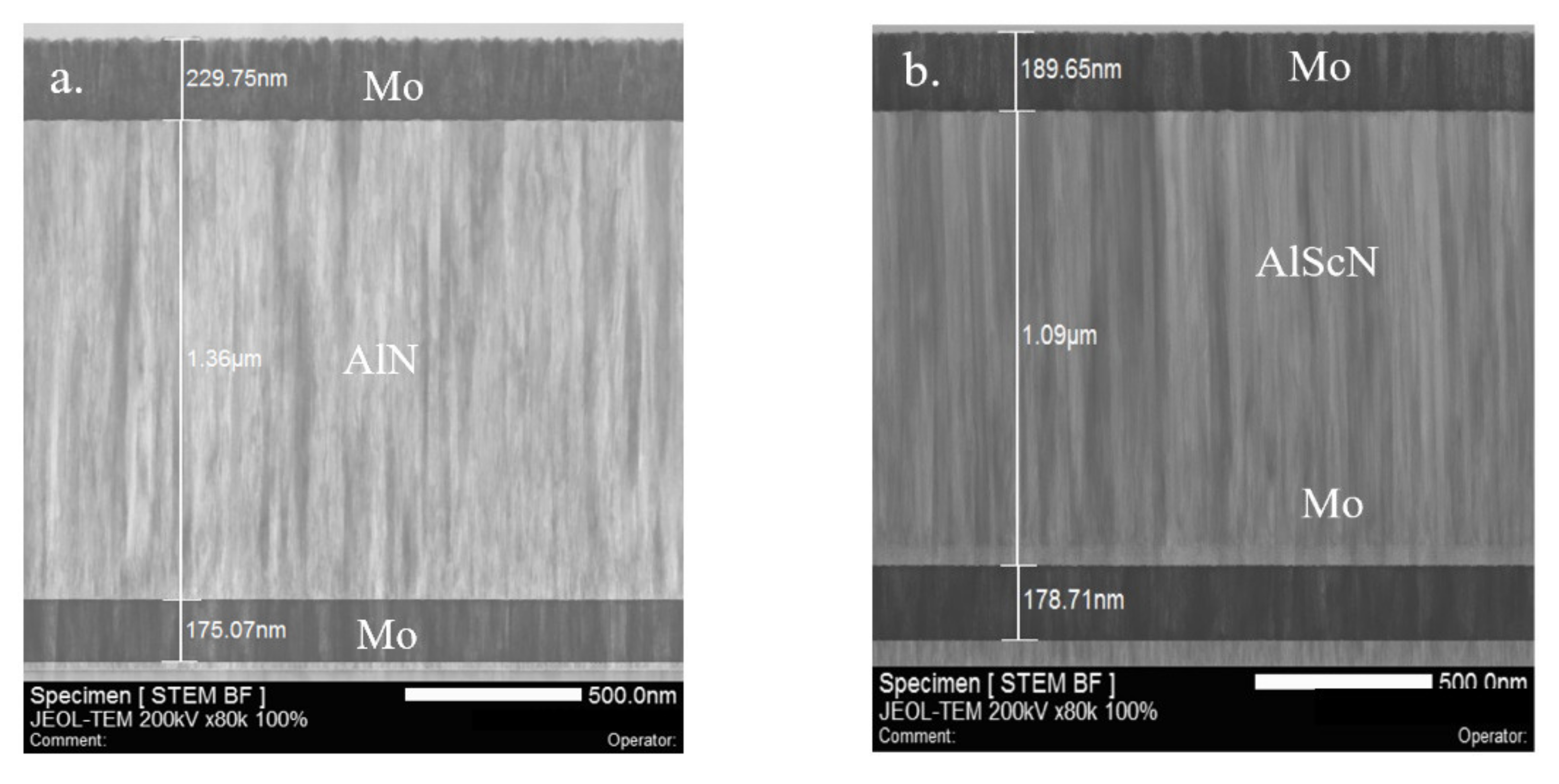
A focused ion beam (FIB) lamella was cut from the investigated PCM in the normal direction of the wafer surface to investigate the microstructure of the AlN and AlScN films. Figure 2a,b show that both the AlN and AlScN films had nearly perfect textured grain orientation along the direction normal to the substrate. Moreover, both films had sub-nm roughness, as identified from the clear sharp contrast for the Mo/AlN interfaces.
As a general rule, the FWHM of polycrystalline AlN thin films should be less than 2° to be used to fabricate high-performance MEMS devices. The X-ray diffraction (XRD) rocking curves can be found in Figure 2c,d for the AlN and AlScN films used in this study, from which the FWHM was found to be 1.32° for AlN and 1.53° for AlScN, respectively. Compared with the FWHM values reported in other studies [20,21], the results for the FWHM of the AlN and AlScN films used in this study confirmed that the piezoelectric film had a high c-axis orientation and good crystal quality.
Crystalline texture and diffraction images of AlN and AlScN were observed by selected area electron diffraction (SAD). The diffraction patterns in the SAD corresponded solely to the swurtzite-type AlN lattice in the highly oriented polycrystalline thin films, thus excluding the presence of metallic Sc crystal clusters. The AlN and AlScN layers both had a point diffraction pattern with (0001) as the preferred orientation parallel to the normal to the substrate (Figure 2e,f). The XRD and SAD results were in good agreement.

3. Results and Discussion

3.1. Piezoelectric Analysis

In this work, two top electrode designs were used for the DBLI test and LDV test, as shown in Figure 3a and Figure 4a, respectively. The square two-port electrode shown in Figure 4a was designed as an inner and outer two-layer electrode to reduce the deformation of the substrate by applying an AC voltage with a phase of 180° to the inner and outer electrodes, respectively (See Supplementary Materials for details of the DBLI test). Additionally, the square electrode was extended in the longitudinal direction to increase the total electrode area, which reduced the influence of substrate deformation while realizing a larger excitation area of the piezoelectric layer. However, a square two-port electrode design with a larger area resulted in measurements that were much larger than the actual d33 value in the DBLI test. According to Sivaramakrishnan et al., the size of the top electrode should be similar to the substrate thickness to obtain consistent piezoelectric parameters [22]. Therefore, the diameter of the single circular electrode was set to 500 μm, which was similar to the thickness of the underlying silicon substrate, as shown in Figure 3a.
First, the longitudinal piezoelectric coefficient d33 of the piezoelectric thin films was extracted by DBLI (aixACCT Systems GmbH, Aachen, Germany). The test schematic diagram can be found in Figure 3. Optionally, a reflective thin film, such as Ti/Au, could be sputtered on the polished surface of the bottom side of the Si substrate to improve the quality of the test signal reflection [22].
A PCM with a single circular electrode design on the same wafer was characterized. Notably, DBLI measurement technology uses double laser beams to eliminate any contribution of substrate bending to d33,f [22]. The device used in the DBLI test is shown in Figure 3a. The DBLI test was applied to the sample, and the results are shown in Figure 3c,d [23]. The results for d33,f were obtained by fitting the average slope of the test results for voltage and displacement, d33,f,AlN = 3.18 pm/V and d33,f,AlScN = 5.18 pm/V, and the test results showed good repeatability (<3%).
Since the accuracy of the test results of DBLI in Figure 3 is not fully verified by other test method, in this study, we only used the d33,f results from DBLI to refine the value ranges of the d33 and d31 simulation parameters in the FEM method, to more effectively obtain the accurate d33 and d31 results. For wurtzite type crystals with known d33 and d31 relationship [20]:
d33/2 < d31 < −d33/2 + 2.2 (pm/V)
Substituting s11,p, s12,p, and s13,p into Formula (5), we obtained d33 greater than d33,f and less than twice the value of d33,f. Therefore, Formula (7) was obtained:
d33,f < d33 < 2d33,f
Substituting d33,f,AlN and d33,f,AlScN from DBLI into Formula (7), we obtained 3.18 pm/V < d33,AlN < 6.36 pm/V and 5.18 pm/V < d33,AlScN < 10.28 pm/V. Substituting the above inequality into Formula (6), we obtained 5.18 pm/V < d33,AlScN < 10.28 pm/V and −5.18 pm/V < d31,AlScN < −2.98 pm/V. Therefore, the simulation parameter sweep range was set as shown in Table 1.
Then, the strain of the thin film material under an applied voltage was tested using LDV (Polytec MSA 500). A 180° phase shifted 65 kHz AC excitation voltage was amplified to 100 V by a high voltage amplifier (Aigtek ATA-2032) and applied to the inner and outer electrodes to excite the piezoelectric thin film and the out-of-plane component of the strain was recorded via LDV (See Supplementary Materials for details of the LDV test). Because the test structure is a complete body structure, the resonance frequency of the test structure can be obtained by simulation, which is about GHz. The test frequency is far away from the resonance point, so the displacement response measured at this frequency reflects the real situation of film strain, and there is no possibility of resonance amplification. Piezoelectric constants were determined by subsequent FEM simulations, which were carried out with COMSOL software. All samples were attached to thick aluminum substrates with stiff insulating epoxy glue, and the aluminum substrates were fixed on the test bench to reduce the pulling effect of the surface deformation on the bottom surface of the substrate to a negligible level.
Figure 4b shows the cross section of the PCM. The materials and dimensions of each layer can be found in Table 2. The 4-inch <100> silicon wafer consisted of a 450-μm silicon substrate and an AlN/AlScN layer with upper and lower Mo electrode interlayers. Table 3 shows the material parameters used in the FEM simulation. According to the calculation method in reference [24], s11,p, s12,p, and s13,p were calculated from elastic constants. The calculation results are listed in Table 3.
Due to symmetry, the simulated structure consisted of two-dimensional boxes representing each layer, as shown in Figure 4c. The thickness of the piezoelectric film was composed of at least 15 quadrilateral elements to form a grid. The finite element calculation was performed under the condition that a voltage of U = 100 V was applied to the gold electrode on the upper surface of the AlScN layer. Figure 4c shows that the 2-port electrodes had opposite deflection displacements, so the substrate bending was reduced to a lower level. A small amount of the electrode displacement excited by the voltage was transferred to the aluminum substrate. Therefore, to improve the accuracy of determining the piezoelectric parameters, the simulation model of the inner and outer two-port electrodes included the aluminum substrate part. Finally, the complete scan result of the displacement along the vertical direction of the centerline on the surface of the piezoelectric film material was extracted into the data set for the measurement and evaluation of the piezoelectric constant.
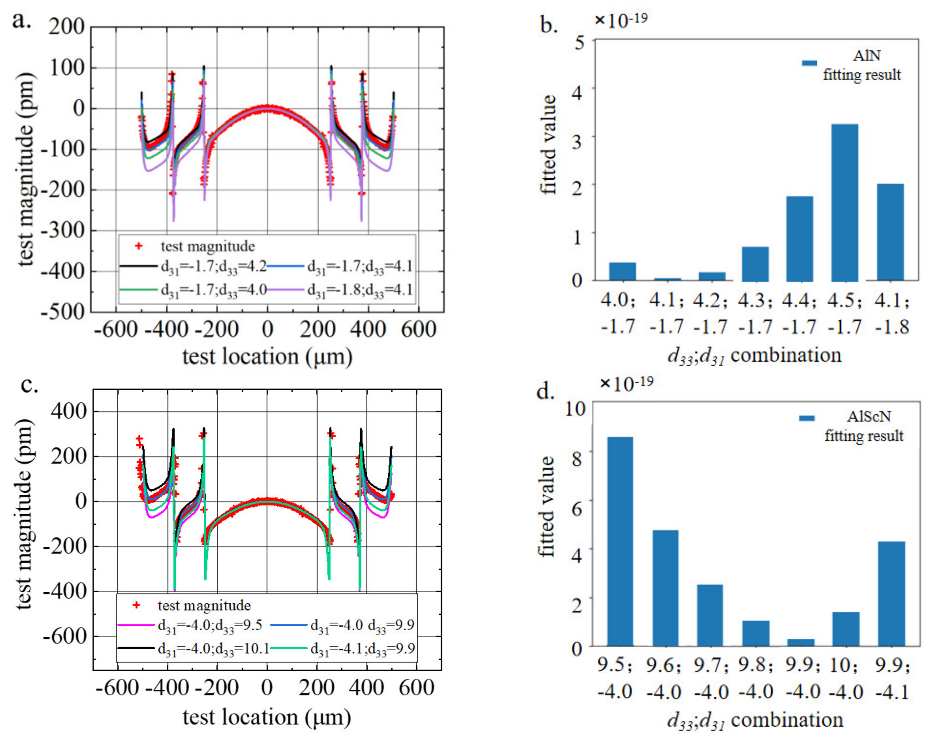
Then, the electrode longitudinal deflection results were measured for the electrodes shown in Figure 4a. We estimated the piezoelectric coefficients of AlN and AlScN. Figure 5a,c compare the images of the deflection measurements and the finite element results under different sets of d33 and d31 parameter combinations.
The fitting between the test and the simulation data was performed by the least squares method. The fitting results for all parameter combinations were compared, and the simulation data for the parameter combination with the smallest calculation result were considered to be the best experimental result. To intuitively obtain the fitting results of each parameter combination, Figure 5b,d compare the least squares results of some parameter combinations. We found that d33,AlN = 4.1 pm/V, d31,AlN = −1.7 pm/V, d33,AlScN = 9.9 pm/V and d31,AlScN = −4.0 pm/V obtained the smallest fitting value. This means that this parameter combination was most consistent with the actual piezoelectric parameter values of the piezoelectric thin film. Therefore, the resulting piezoelectric coefficients for the AlN samples were d33 = 4.1 pm/V and d31 = −1.7 pm/V, agreeing excellent with those reported by Hernando et al. [15] and Mayrhofer et al. [18]. The resulting piezoelectric coefficients for the AlScN samples were d33 = 9.9 pm/V and d31 = −4.0 pm/V. These results agree well with earlier measurements of d33 of AlScN (d33 ~ 10 pm/V) reported by Akiyama et al. [11]. In addition, the values for d33 and d31 are in line with results from ab initio calculations that predict values for AlScN of about d31 ~ −5 pm/V and d33 ~ 10 pm/V [25].
Substituting the measured d33 and d31 results into Formula 5, we obtained d33,f,AlN = 3.061 pm/V and d33,f,AlScN = 7.220 pm/V, which were very similar to the d33,f value measured by in situ XRD below.

3.2. Verification of the Results

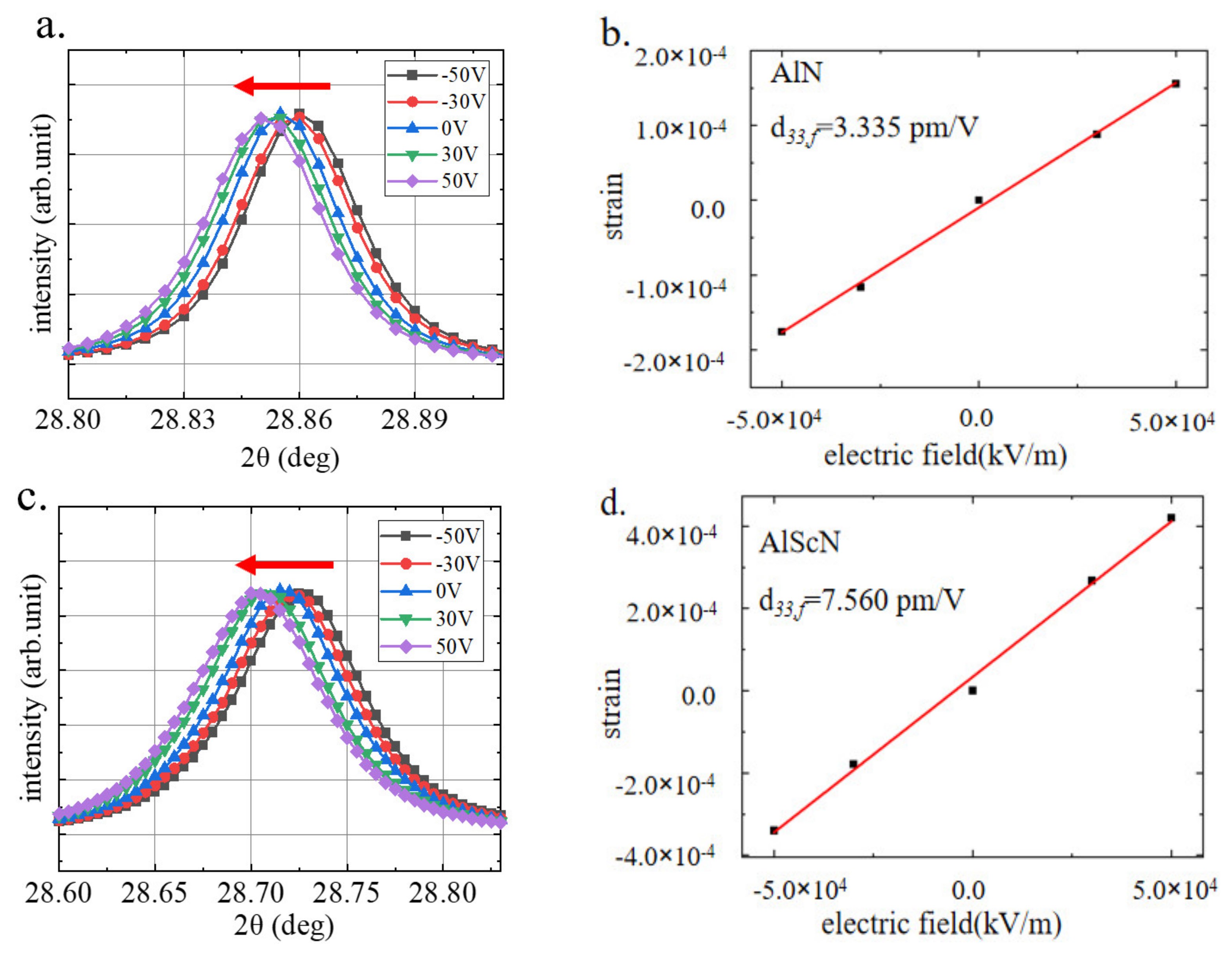
To verify the accuracy of the piezoelectric parameters obtained by the abovementioned FEM method, we used synchrotron X-ray diffraction at the Shanghai Synchrotron Radiation Facility (SSRF) to observe the reversible elongation and contraction of the lattice parameters of the same batch of samples under an external electric field. The in-situ XRD experiments were carried out using synchrotron radiation with a 10.48 keV photon energy (λ = 0.12438 nm) performed on the BL02U beamline, with a beam diameter of 300 μm. Figure 6 shows the peaks for the AlN and AlScN films under different DC voltages (See Supplementary Materials for details of the in-situ XRD test). As the negative voltage increased, the diffraction peak moved to a lower angle and vice versa.
The change in the lattice length under the action of the longitudinal electric field accurately represented the longitudinal piezoelectric coefficient d33 of the material. To obtain accurate calculation results, the film thickness shown in Figure 2a,b was used in the calculation.
The out-of-plane XRD pattern results are shown in Figure 6. According to the relationship between the electric field and the field-induced strain, the effective longitudinal piezoelectric constants d33,f,AlN = 3.335 pm/V and d33,f,AlScN = 7.560 pm/V were estimated; they were very close to the value of d33,f calculated by our proposed method. At present, there is no team has characterized the d33 coefficient of AlN and AlScN films by synchrotron X-ray diffraction. However, according to the existing research, the accuracy of synchrotron X-ray diffraction test results has been well proved [26].
It’s worth noting that, the growth process of piezoelectric film inevitably introduces residual stress into the film, and according to the research of Berfield, T.A et al. [27], the magnitude of piezoelectric response will decrease with the increase of residual stress. In this paper, in-situ XRD is used to characterize the effective forward piezoelectric coefficient d33. Because the test results are obtained by applying different DC bias on the same sample for multiple measurements, the relationship between the obtained strain and the applied voltage is a relative value. Therefore, in-situ XRD can eliminate the influence of residual stress on piezoelectric test results.
SEM images of the cantilever beam structure used in the test and the material and thickness of each layer of the cantilever are shown in Figure 7a,b. The influence of the length and thickness of the cantilever on the measurement results has been given by Dekkers et al. [28]. We made 200 μm, 300 μm, 400 μm and 500 μm cantilevers and measured their displacement at resonance; the calculated d31 values are marked in Figure 7c (See Supplementary Materials for details of the cantilevers test). We found that the law of the obtained d31 values was the same as that found by Dekkers et al., and the d31 result obtained by the 400 μm cantilever was closest to the true value. Formula 8 was used to obtain the effective transverse piezoelectric coefficients of the piezoelectric films: d31,AlN = −1.68 pm/V and d31,AlScN = −3.89 pm/V.
δ = 3 d 31 s s s p t s t s + t p L 2 V s 2 s t 4 p + 4 s s s p t s t 3 p + 6 s s s p t 2 s t 2 p + 4 s s s p t 3 s t p + s p t 4 s
where δ is the cantilever displacement, ss and sp are the mechanical compliances of the substrate and the AlScN, ts and tp are the thicknesses of the substrate and the AlScN respectively, L is the length of the cantilever and V is the excitation voltage. The compliance is related to Young’s modulus E by s = 1/E. The values for Young’s moduli are listed in Table 3. The material and thickness of each layer used in the calculation of the cantilever are listed in Table 4. The thickness of the Mo electrodes had little effect on the results, and it is given here to guide the fabrication of devices.
Our results are very close to those obtained by Stoecke et al. (d31,AlN ~ −1.5 pm/V) [29]. The test results can provide reference value for the test and research of AlN cantilever beam method.
Table 5 shows that the difference between the d31 result obtained by the cantilever method and the d31 results obtained by the LDV method was within 10%, which verified the accuracy of the LDV method.

4. Conclusions

In this paper, we proposed a new test method that combined DBLI and LDV-FEM to improve the extraction efficiency of transverse and longitudinal piezoelectric coefficients. The on-chip integrated process control monitor (PCM) test structure was fabricated with the flow sheet of the MEMS device without creating a discrete test structure. This quick approach used few MEMS process steps to simultaneously evaluate the piezoelectric coefficients of the AlN and AlScN thin films. The pure AlN and 20% scandium-doped AlScN films grown by reactive magnetron sputtering were tested; the longitudinal effective piezoelectric coefficients were d33,AlN = 4.1 pm/V and d33,AlScN = 9.9 pm/V, and the transverse effective piezoelectric coefficients were d31,AlN = −1.7 pm/V and d31,AlScN = −4.0 pm/V. In situ XRD measurements of the film were conducted using the Shanghai synchrotron radiation source to verify the accuracy of the d33 results, and the cantilever method was used to verify the accuracy of the d31 results. As shown in Table 5, the errors of the various test methods were within 10%, which proved the accuracy of our new method. This work provided a reliable and efficient method for the characterization of piezoelectric films and strong support for the design and simulation of ScxAl1−xN-based piezoelectric MEMS devices with enhanced electromechanical properties.

Supplementary Materials

The following supporting information can be downloaded at https://www.mdpi.com/article/10.3390/mi13040581/s1: Experimental details of the LDV, DBLI, SSRF and cantilever tests.

Author Contributions

Conceptualization, supervision, writing—review and editing, Z.W. and Y.W.; methodology, data curation, writing—original draft preparation, H.Z., Y.W.; validation, investigation, visualization, L.W., Y.L., H.C.; project administration, funding acquisition, Z.W. All authors have read and agreed to the published version of the manuscript.

Funding

This research was funded by the National Key R&D Program of China (No. 2021YFB3202500) and the R&D Program of Scientific Instruments and Equipment, Chinese Academy of Sciences (No. YJKYYQ20190026).

Data Availability Statement

Data are available from the authors on request.

Acknowledgments

The authors thank Henghui Cai from the Shanghai Institute of Ceramics, Chinese Academy of Sciences, for DBLI sample preparation and analysis and Huamao Lin formally from Shanghai Industrial μTechnology Research Institute for AlN/AlScN sample preparation, Xiaolong Li from the Shanghai Synchrotron Radiation Facility for in situ XRD characterization, Liuyong Wang and from the SIMIT for STEM and SAD preparation, Weimin Li from Shanghai Institute of IC Materials for discussion and encouragement, and Lingli Chen, Yubo Zhu and Ruidong Qin for help with in situ XRD characterization.

Conflicts of Interest

The authors declare no conflict of interest.

References

  1. Uehara, K.; Tsubouchi, K. GHz-band acoustic wave device for wireless communication using aluminum nitride film. Rec. Electr. Commun. Eng. Conversazione Tokohu Univ. 2006, 74, 32–35. [Google Scholar]
  2. Alfadhel, A.; Jing, O.; Cormier, D.; Borkholder, D.A. Enhanced properties of aerosol jet printed PZT: Towards realizing flexible automotive sensors. 2020 IEEE Sens. 2020, 4, 4. [Google Scholar]
  3. Shin, E.; Yeo, H.G.; Yeon, A.; Jin, C.; Park, W.; Lee, S.C.; Choi, H. Development of a High-Density Piezoelectric Micromachined Ultrasonic Transducer Array Based on Patterned Aluminum Nitride Thin Film. Micromachines 2020, 11, 623. [Google Scholar] [CrossRef] [PubMed]
  4. Lv, H.; Huang, Y.; Ai, Y.; Liu, Z.; Lin, D.; Cheng, Z.; Jia, L.; Guo, B.; Dong, B.; Zhang, Y. An Experimental and Theoretical Study of Impact of Device Parameters on Performance of AlN/Sapphire-Based SAW Temperature Sensors. Micromachines 2022, 13, 40. [Google Scholar]
  5. Sun, C.H.; Liu, Y.F.; Li, B.L.; Su, W.Q.; Luo, M.Z.; Du, G.F.; Wu, Y.M. Modeling and Optimization of a Novel ScAlN-Based MEMS Scanning Mirror with Large Static and Dynamic Two-Axis Tilting Angles. Sensors 2021, 21, 2213. [Google Scholar]
  6. Liu, J.M.; Pan, B.; Chan, H.L.W.; Zhu, S.N.; Zhu, Y.Y.; Liu, Z.G. Piezoelectric coefficient measurement of piezoelectric thin films: An overview. Mater. Chem. Phys. 2002, 75, 12–18. [Google Scholar] [CrossRef]
  7. Gangidi, P.; Gupta, N. Optimal selection of dielectric film in piezoelectric MEMS microphone. Microsyst. Technol. Micro Nanosyst. Inf. Storage Process. Syst. 2019, 25, 4227–4235. [Google Scholar]
  8. Iborra, E.; Clement, M.; Sangrador, J.; Sanz-Hervas, A.; Vergara, L.; Aguilar, M. Effect of particle bombardment on the orientation and the residual stress of sputtered AlN films for SAW devices. IEEE Trans. Ultrason. Ferroelectr. Freq. Control 2004, 51, 352–358. [Google Scholar]
  9. Guenthner, S.; Egretzberger, M.; Kugi, A.; Kapser, K.; Hartmann, B.; Schmid, U.; Seidel, H. Compensation of parasitic effects for a silicon tuning fork gyroscope. IEEE Sens. J. 2006, 6, 596–604. [Google Scholar] [CrossRef]
  10. Akiyama, M.; Tabaru, T.; Nishikubo, K.; Teshigahara, A.; Kano, K. Preparation of scandium aluminum nitride thin films by using scandium aluminum alloy sputtering target and design of experiments. J. Ceram. Soc. Jpn. 2010, 118, 1166–1169. [Google Scholar] [CrossRef] [Green Version]
  11. Akiyama, M.; Kamohara, T.; Kano, K.; Teshigahara, A.; Takeuchi, Y.; Kawahara, N. Enhancement of Piezoelectric Response in Scandium Aluminum Nitride Alloy Thin Films Prepared by Dual Reactive Cosputtering. Adv. Mater. 2009, 21, 593. [Google Scholar] [CrossRef]
  12. Lefki, K.; Dormans, G. Measurement of piezoelectric coefficients of ferroelectric thin films. J. Appl. Phys. 1994, 76, 1764–1767. [Google Scholar] [CrossRef]
  13. Chun, D.-M.; Sato, M.; Kanno, I. Precise measurement of the transverse piezoelectric coefficient for thin films on anisotropic substrate. J. Appl. Phys. 2013, 113, 044111. [Google Scholar] [CrossRef]
  14. Campanella, H. Acoustic Wave and Electromechanical Resonators; Concept to Key Applications; IEEE: Piscataway, NJ, USA, 2010. [Google Scholar]
  15. Hernando, J.; Sanchez-Rojas, J.L.; Gonza?Lez-Castilla, S.; Iborra, E.; Ababneh, A.; Schmid, U. Simulation and laser vibrometry characterization of piezoelectric AlN thin films. J. Appl. Phys. 2008, 104, 053502. [Google Scholar] [CrossRef] [Green Version]
  16. Kholkin, A.L.; Wutchrich, C.; Taylor, D.V.; Setter, N. Interferometric measurements of electric field-induced displacements in piezoelectric thin films. Rev. Sci. Instrum. 1996, 67, 1935–1941. [Google Scholar] [CrossRef]
  17. Sivaramakrishnan, S.; Mardilovich, P.; Schmitz-Kempen, T.; Tiedke, S. Concurrent wafer-level measurement of longitudinal and transverse effective piezoelectric coefficients (d(33,f) and e(31,f)) by double beam laser interferometry. J. Appl. Phys. 2018, 123, 014103. [Google Scholar] [CrossRef]
  18. Mayrhofer, P.M.; Euchner, H.; Bittner, A.; Schmid, U. Circular test structure for the determination of piezoelectric constants of ScxAl1-xN thin films applying Laser Doppler Vibrometry and FEM simulations. Sens. Actuators A-Phys. 2015, 222, 301–308. [Google Scholar] [CrossRef] [Green Version]
  19. Qi, W.; Lu, Y.; Fung, S.; Jiang, X.; Horsley, D. Scandium Doped Aluminum Nitride Based Piezoelectric Micromachined Ultrasound Transducers. In Proceedings of the Hilton Head Workshop 2016: A Solid-State Sensors, Actuators and Microsystems Workshop, Hilton Head, SC, USA, 5–9 June 2016. [Google Scholar]
  20. Bernardini, F.; Fiorentini, V. First-principles calculation of the piezoelectric tensor (d)over-left-right-arrow of III–V nitrides. Appl. Phys. Lett. 2002, 80, 4145–4147. [Google Scholar] [CrossRef]
  21. Mayrhofer, P.M.; Wistrela, E.; Schneider, M.; Bittner, A.; Schmid, U. Precise determination of d(33) and d(31) from piezoelectric deflection measurements and 2D FEM simulations applied to ScxAl1-xN. In Proceedings of the 30th Eurosensors Conference, Budapest, Hungary, 4–7 September 2016; pp. 876–879. [Google Scholar]
  22. Sivaramakrishnan, S.; Mardilovich, P.; Mason, A.; Roelofs, A.; Schmitz-Kempen, T.; Tiedke, S. Electrode size dependence of piezoelectric response of lead zirconate titanate thin films measured by double beam laser interferometry. Appl. Phys. Lett. 2013, 103, 132904. [Google Scholar] [CrossRef] [Green Version]
  23. Schmitz-Kempen, T.; Tiedke, S.; Lisec, T.; Stoppel, F.; Mardilovich, P.; Trolier-McKinstry, S.; Sivaramakrishnan, S.; Muralt, P. Comparable Measurements and Modeling of Piezoelectric Thin Films for MEMS application. In Proceedings of the IEEE International Symposium on the Applications of Ferroelectric/Workshop on the Piezoresponse Force Microscopy (ISAF/PFM), Prague, Czech Republic, 21–25 July 2013; pp. 211–213. [Google Scholar]
  24. Tsubouchi, K.; Mikoshiba, N. Zero-Temperature-Coefficient SAW Devices on AlN Epitaxial Films. IEEE Trans. Sonics 1985, 32, 634–644. [Google Scholar] [CrossRef]
  25. Umeda, K.; Kawai, H.; Honda, A.; Akiyama, M.; Kato, T.; Fukura, T. Piezoelectric Properties of Scaln Thin Films for Piezo-Mems Devices. In Proceedings of the 26th IEEE International Conference on Micro Electro Mechanical Systems (MEMS), Taipei, Taiwan, 20–24 January 2013; pp. 733–736. [Google Scholar]
  26. Tan, G.; Maruyama, K.; Kanamitsu, Y.; Nishioka, S.; Ozaki, T.; Umegaki, T.; Hida, H.; Kanno, I. Crystallographic contributions to piezoelectric properties in PZT thin films. Sci. Rep. 2019, 9, 7309. [Google Scholar] [CrossRef]
  27. Berfield, T.A.; Ong, R.J.; Payne, D.A.; Sottos, N.R. Residual stress effects on piezoelectric response of sol-gel derived PZT thin films. Dep. Theor. Appl. Mech. 2007, 101, 024102. [Google Scholar]
  28. Dekkers, M.; Boschker, H.; Van Zalk, M.; Nguyen, M.; Nazeer, H.; Houwman, E.; Rijnders, G. The significance of the piezoelectric coefficient d31, eff determined from cantilever structures. J. Micromech. Microeng. 2012, 23, 025008. [Google Scholar] [CrossRef] [Green Version]
  29. Stoeckel, C.; Kaufmann, C.; Hahn, R.; Schulze, R.; Billep, D.; Gessner, T. Pulsed DC magnetron sputtered piezoelectric thin film aluminum nitride-Technology and piezoelectric properties. J. Appl. Phys. 2014, 116, 034102. [Google Scholar] [CrossRef]
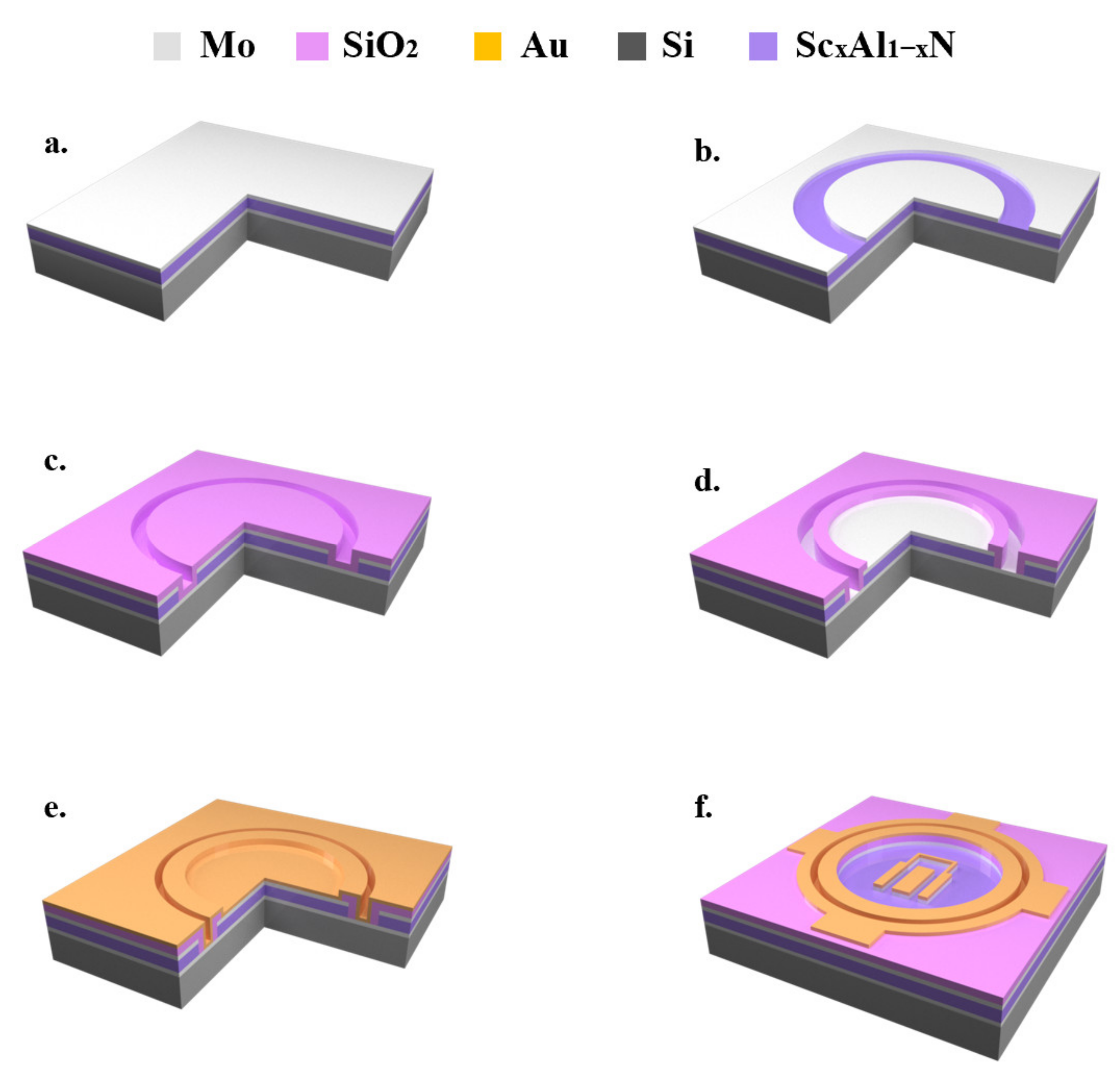
Figure 1. The process flow of the PCM structure. (a) a stack of Mo/AlN(AlScN)/Mo is deposited by magnetron sputtering; (b) a 0.2 µm Mo top layer is patterned and etched as a hard mask for the underlying AlN/AlScN layer etching; (c) a 1 µm layer of SiO2 is deposited by PECVD; (d) the top and bottom electrodes are exposed after SiO2 patterning; (e) a 0.5 µm layer of Ti/Au was deposited; (f) the top Au electrode was patterned for electrical connection.
Micromachines 13 00581 g001
Figure 2. (a) Scanning transmission electron microscopy (STEM) image of the Mo-AlN-Mo structure; (b) STEM image of the Mo-AlScN-Mo structure; (c) Rocking curves of the AlN film; (d) rocking curves of the AlScN film; (e) selected area diffraction (SAD) pattern of AlN; (f) SAD pattern of AlScN.
Micromachines 13 00581 g002aMicromachines 13 00581 g002b
Figure 3. (a) The scanning electron microscope (SEM) image of the device used in DBLI test. (b) Schematic diagram of DBLI test system and test principle; (c) DBLI test results of AlN and (d) AlScN.
Micromachines 13 00581 g003
Figure 4. (a) SEM image of the device used in the LDV test; (b) 2D cross-sectional view of the 2-port electrode design used as input for the FEM simulations; (c) FEM results for the local displacement perpendicular to the wafer surface.
Micromachines 13 00581 g004
Figure 5. (a,b) AlN and (c,d) AlScN test and simulation data fitting results.
Micromachines 13 00581 g005
Figure 6. Out-of-plane XRD patterns of the (a) AlN and (b) AlScN thin films obtained for the (002) peak under varying DC voltages; The d33,f linear fit results of (c) AlN and (d) AlScN thin films.
Micromachines 13 00581 g006
Figure 7. (a) SEM image of the cantilever beam; (b) the test and simulation results for AlN and AlScN cantilever beams with different lengths of AlN and AlScN; (c) the test results of the AlN and AlScN cantilevers.
Micromachines 13 00581 g007
Table 1. The simulation parameter range settings.
MaterialRange of d31 [pm/V]Range of d33 [pm/V]Step Length [pm/V]
AlN−3.18 to −0.983.18 to 6.360.1
AlScN−5.18 to −2.985.18 to 10.280.1
Table 2. Input parameters of the simulation model for the FEM.
LayerMaterialThickness [nm]GapWidth [μm]
1Au200 nma250 μm
2Mo200 nmb125 μm
3AlN/AlScN1.36 μm/1.09 μmc125 μm
4Mo200 nm//
5Si450 μm//
6Al2 mm//
Table 3. The material parameters used in FEM simulation.
MaterialPropertyValueUnits
Anisotropic Si <100>Young’s modulus130[GPa]
Poisson’s ratio0.28/
AlN [24]Young’s modulus338[GPa]
c11 = c22345[GPa]
c33395[GPa]
c12125[GPa]
c13120[GPa]
c44 = c55118[GPa]
c66 = (c11c12)/2110[GPa]
s11 = s223.53[10−12 m2/N]
s12−1.01[10−12 m2/N]
s13−0.77[10−12 m2/N]
s333[10−12 m2/N]
s44 = s558.48[10−12 m2/N]
s669.09[10−12 m2/N]
Sc0.2Al0.8N [18]Young’s modulus230[GPa]
c11 = c22325[GPa]
c33279[GPa]
c12138[GPa]
c13131[GPa]
c44 = c5599[GPa]
c66 = (c11c12)/294[GPa]
s11 = s224.14[10−12 m2/N]
s12−1.02[10−12 m2/N]
s13−1.38[10−12 m2/N]
s334.88[10−12 m2/N]
s44 = s5510.1[10−12 m2/N]
s6610.6[10−12 m2/N]
Table 4. The material and thickness of each layer used in the calculation of the cantilever.
LayerMaterialThicknessWidth (W)
1Mo200 [nm]35 [μm]
2AlN (AlScN)1.36 [μm] (1.09 [μm])35 [μm]
3Mo200 [nm]35 [μm]
4Si30 [μm]35 [μm]
Table 5. Comparison of different test methods.
Cantilever Method [pm/V]In-Situ XRD [pm/V]LDV-FEM [pm/V]
AlN d33,f/3.3353.061
AlN d31−1.68/−1.7
AlScN d33,f/7.5607.22
AlScN d31−3.89/−4.0
Publisher’s Note: MDPI stays neutral with regard to jurisdictional claims in published maps and institutional affiliations.