Article

An Efficient 24–30 GHz GaN-on-Si Driver Amplifier Using Synthesized Matching Networks

1
School of Information Engineering, Guangdong University of Technology, Guangzhou 510006, China
2
School of Integrated Circuits, Guangdong University of Technology, Guangzhou 510006, China
*
Author to whom correspondence should be addressed.
Micromachines 2023, 14(1), 175; https://doi.org/10.3390/mi14010175
Submission received: 24 November 2022 / Revised: 2 January 2023 / Accepted: 6 January 2023 / Published: 10 January 2023
(This article belongs to the Special Issue Wireless Transceiver Design for RF/MM Waves and THz Communication)

Abstract

:
This paper presents a broadband GaN microwave monolithic integrated circuit driver amplifier (MMIC DA) with compact dimensions of 1.65 mm × 0.78 mm for 5G millimeter-wave communication. The optimal impedance domain satisfying the preset goals was first acquired using the simplified load-pull procedure and small-signal simulations, followed by a weighted average method to determine the reference center matching point from which the optimal intrinsic load can be deduced. By means of de-embedding load-pull contours, modeling based on theoretical analysis, and simulation fitting for parameter identification, the nonlinear output capacitance and a series RLC model circuit approximating the input impedance response of the stabilized transistor were extracted. Under the design principle of fully absorbing the parasitic parameters of the device, explicit formulas and tabulated methods related to the Chebyshev impedance transformer were applied to construct filter-based synthesized matching networks at each stage and finally convert them into an implementable mixed-element form via the single-frequency equivalence technique. Measured on-wafer pulsed results for the proposed two-stage DA across 24–30 GHz demonstrated up to 31.1 dBm of saturated output power (Psat) with less than 1 dB total fluctuation, 19.3 ± 1 dB of small-signal gain, and 39.8% of peak power-added efficiency (PAE) at the mid-frequency.

1. Introduction

During this period of coexistence with the COVID-19 pandemic, online education and cloud offices are on the rise, greatly supported by the extensive 5G wireless infrastructure. Commercial 5G networks have thus far been deployed chiefly in the popular but congested sub-6 GHz frequency range 1 (FR1), with an accelerated evolution toward millimeter-wave (mmW) bands, which possess an abundant spectrum with much wider bandwidths to address the ever-growing demand for mobile data traffic. In particular, the 24–30 GHz range spanning the overlapping bands n257, n258, and n261 that has been planned, licensed, and launched the most by nations worldwide is the focus [1]. Despite their tremendous potential, due to the short wavelengths, mmW communications have some natural drawbacks, such as significant propagation loss and the susceptibility to blockage. Hence, to remedy the lack of mmW signal coverage, the rated output power (Pout) levels of 5G microcells are often higher. Under such circumstances, a driver amplifier (DA) unit is needed to provide good linearity or efficiency performance as the gain stage prior to the final power amplifier (PA) in an RF transmitter chain [2].
Given that frequency allocations differ by country, a promising low-cost solution from a market perspective is a broadband MMIC DA capable of operating over multiple 3GPP bands in 5G NR FR2, facilitating both the integration and robustness of the front-end system. However, obtaining a sufficient bandwidth, while maintaining decent efficiency in the smallest possible physical footprint poses a challenge to amplifier design because these requirements are mutually restrictive. Leaving aside architectural schemes such as the well-known Doherty and outphasing amplifiers, which are mainly intended to improve the average efficiency within a limited bandwidth and also necessitate substantial components, a regular single-way structure would be more attractive in terms of implementation complexity, for which, the primary efficiency enhancement technique is the so-called waveform engineering. Conventional harmonic-tuned class-F/F−1 PAs strive to create a specific impedance environment that shapes output V–I waveforms with less crossover for greater absolute efficiency but a narrow fractional bandwidth (FBW) [3]. Continuous class-J PAs, proposed later, subtly mitigate this shortcoming through the “design space” concept, which alleviates stringent harmonic impedance requirements, reaching the same high efficiency as those in the normal class-B mode by only manipulating up to the second harmonic load [4,5]. These amplifiers, however, are typically biased at a class-B or deep class-AB condition and added with harmonic control circuitry, resulting in a poor linear drive capability and higher area consumption. Therefore, we need to focus on the broadband aspect to find a satisfactory solution. More specifically, we should look for appropriate matching approaches to present the optimal complex load and source impedances to the device within the designated broadband. The simplified real-frequency technique (SRFT) directly processes gathered discrete load data with computer-aided design (CAD) programs, solving least-squares problems to build broadband matching networks (MNs) without modeling the load or relying on expertise to predefine a proper equalizer topology [6]. However, when the classical Levenberg–Marquardt (LM) algorithm is applied to optimize the transducer power gain function, the convergence speed and results are sensitive to the initial assignment of multiple independent variables; substituting with a more robust genetic or hybrid algorithm can help search for a global optimal solution [7,8], but at the price of increased computational complexity, which limits the practicality of the SRFT. Another category of analytical methodology, based on filter synthesis, yields closed-form solutions for simple loads of RC, RL, and RLC [9,10,11], which is mature in theory and easier to implement than CAD-dependent numerical optimization. MNs with different passband properties can be configured according to the load composition, the mainstream being Butterworth, Chebyshev, and Elliptic types and their derivatives [11,12,13,14,15,16]. The filter-matching method is flexible enough to absorb parasitic parameters at both the input and the output of the transistor, enabling broadband impedance transformation and strengthening amplifier band selectivity, while reducing harmonic energy loss.
Last but not the least, in MMIC performance, device technology is the bottleneck because the radical way to extend the bandwidth is to reduce the MN’s impedance transformation ratio (ITR), and attaining the requisite amount of forward gain with fewer amplification stages effectively promotes efficiency. Compared to the widespread Si- and GaAs-based semiconductors, emerging GaN high-electron-mobility transistors (HEMTs) have a large material bandgap (3.4 eV) and excellent thermal tolerance, allowing them to run at elevated drain voltages, power densities, and ambient temperatures and thus support smaller form factors. Moreover, they feature a high electron saturation velocity and port resistances with low parasitic capacitances, making them ideal for broadband high-efficiency amplifier designs in the mmW regime [17,18,19,20].
The main scope of this paper is to present a comprehensive procedure of a small-scale 1-watt GaN-on-Si DA covering the range of 24–30 GHz, which is rarely reported in most of the published GaN MMIC literature. On the basis of the optimal impedance domain determined by simplified load-pull and small-signal simulations, together with equivalent input and output impedance models of the stabilized device, the filter synthesis theory was applied to complete the design of MNs so that power cells could perform well. The experimental results of the proposed DA are summarized and compared to those from recently published studies.

2. Circuit Design Considerations

The adopted technology is OMMIC’s (OMMIC SAS, Limeil-Brévannes, France) 0.1 μm double-heterojunction AlN/GaN/AlGaN HEMT process known as D01GH, based on a 3-inch high-resistivity silicon substrate thinned down to 100 μm with a dielectric constant εr of 11.7 and a loss tangent tg(δ) of 0.015. As depicted in Figure 1, it uses in situ passivation to avoid memory effects and regrown non-alloyed ohmic contacts to minimize access resistance. The thin AlN barrier serves to diminish short-channel effects, whereas the AlGaN back barrier improves electron confinement. Mushroom gates of 100-nm-length and a short gate–source distance enable the cutoff frequency (fT, i.e., f @ |H21| = 1) to exceed 100 GHz. The typical RF power density is around 3.3 W/mm @ 30 GHz but can go up to 5.7 W/mm for a recommended bias supply VD of 12 V, with a gate–drain breakdown voltage of 36 V. Depletion-mode transistors have been fully modeled, taking into account the electro-thermal nonlinear attribute. Various passive components, including spiral inductors, NiCr thin-film resistors (40 Ω/□), GaN resistors (400 Ω/□), and two types of MIM capacitors (50 pF/mm2 and 400 pF/mm2), via holes and microstrip lines with metal thickness options of 1.25 μm or 2.5 μm, are available in the foundry design kit [21].
The process we chose is built on a Si platform rather than the general silicon carbide (SiC) one, which has superior thermal conductivity along with low loss. On the one hand, the required power levels for 5G mmW applications make the adoption of a Si substrate feasible, and the other major reason is that SiC remains expensive and subject to export controls, whereas Si-based GaN is relatively cheap, mature enough, and compatible with heterogeneous integration with SiGe/CMOS [22]. It offers a competitive performance and the potential for large economies of scale, opening up the possibility of a realistic volume production of 5G MMICs.

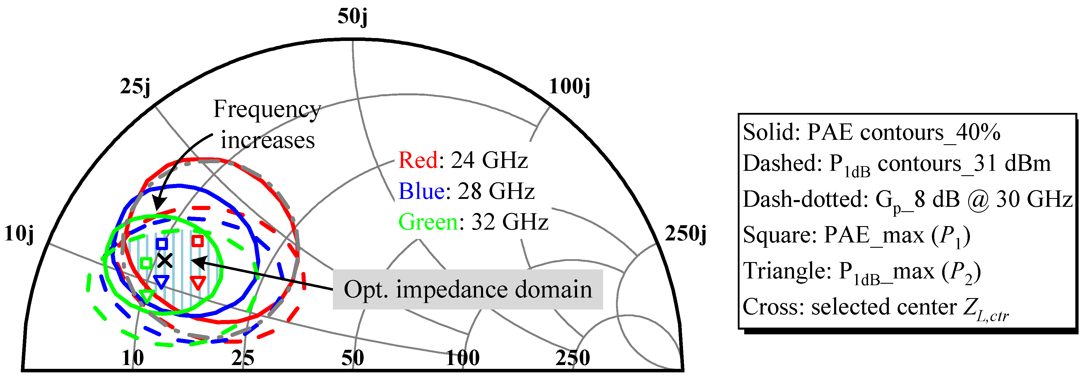
2.1. Fundamental Load-Pull Analysis and Determination of the Optimal Impedance Domain

In consideration of the maximum available gain of transistors, estimated transmission link loss, process variation, and design redundancy, a cascaded two-stage common-source architecture was employed for the DA. Transistor peripheries were staged at a ratio of 1:2, with a 46 × 8 μm cell chosen for the latter stage, to meet the specifications of 1 W Psat with over 30% PAE and beyond 18 dB of linear gain. Due to the nonlinear nature of the device and essentially the output parasitic capacitance Cout, which strongly depends on the operating conditions and transistor geometry, the trajectory formed by connecting the optimal load impedance points ZL,opt obtained through load-pull incrementally by frequency travels counterclockwise when mapped on the Smith chart. However, the recorded impedance locus ZL(f) after transforming the standard 50 Ω by the output matching network (OMN) rotates in the reverse direction with increasing frequency compared to the former. Consequently, even if these two profiles happen to be exactly congruent, phase mismatch will exist for all but one frequency. This unfavorable phenomenon of opposite impedance rotation explains why the amplifier is prone to severe mismatch at and near the edge frequencies of the wide target band, leading to a dramatic deterioration in performance, thus troubling the design of the broadband MN. Instead of attempting to track the frequency-dependent ZL,opt over broadband at the expense of a high component overhead, as in the common strategy, we defined an optimal impedance domain that fulfills the preset goals of PAE > 40%, P1dB > 31 dBm, and output-stage gain > 8 dB. Meanwhile, a compromised center impedance ZL,ctr was identified. The DA’s broadband output capability is basically assured as long as the in-band ZL(f) rotates in a knotted shape around ZL,ctr and falls inside the prescribed constraint space. In addition, considering that the transistor’s gain roll-off characteristics and the actual bandwidth may narrow or frequency-shift from evaluation, the circuit-level design should prioritize an upper-frequency performance, while introducing some low-frequency mismatch to enhance the broadband effect via stagger-tuning for a balanced large-signal response [17].
In mmW bands, Cout shorts out most of the harmonic contents. Therefore, sophisticated harmonic control is no longer viable. As harmonics are far from the passband that can be readily suppressed by a low-pass OMN, the impacts of harmonic loads were first ignored in the course of successive single-tone load-pull simulations by initializing them and source harmonic terminations as open-circuit (e.g., 1 kΩ). It is worth mentioning that a simplified alternative was used here, unlike the conventional process, where the load-pull needs to be iterated with the source-pull to get optimal convergence results. We regarded the HEMT with a parallel RC stabilization network as a new cell, figuring out the voltage-to-current ratio at the equivalent gate node when the cell is excited to the P1dB state by a continuous-wave (CW) signal to derive the fundamental input impedance Zin,fund and then took its conjugate as the source impedance ZS,fund. Since the device’s non-unilateral operation and PAE is more critical, ZS,fund must be updated with the variation of ZL,opt picked at the best PAE for each iteration until the two, which interact, cease to change, i.e., each converges to a certain fixed value. Table 1 compares the conventional and simplified load-pull scripts conducted on the last stage at 24 GHz, 28 GHz, and the extended corner of 32 GHz under the same simulation conditions. There is only a negligible difference in the PAE between them, and the corresponding ZL,opt are identical, so the source-pull step for seeking the optimal source impedance ZS,opt can be omitted to facilitate a more in-depth load analysis with guaranteed correctness.
With this simplified method, joint small-signal simulations for generating constant power gain (GP) circles resulting from load mismatch allow the rapid determination of the wanted optimal impedance domain, shaded in Figure 2. About 2/3 of its boundaries are bound by the contours of PAE and P1dB at 32 GHz due to intensifying parasitic effects (mainly Cout) that cause the contours to move counterclockwise toward the real axis of the Smith chart and gradually shrink as the frequency increases. In addition, the design margin of 2 GHz extended to higher frequencies is an experience-based trade-off and the concentric circle distribution of Gp outcomes in Figure 2 is drawn only for the inner circle at 30 GHz, which is just externally tangent to the optimal domain where three groups of contours overlap. The best performance marks P1 and P2, wrapped around the PAE and P1dB contours, respectively, do not coincide, and they each become closer at higher fundamentals, which in turn are farther apart from one another at the lower side. To accommodate the uneven dispersion of contour peaks, a two-round weighted average calculation was proposed to identify the suitable ZL,ctr. In the beginning, a weighted interpolation was carried out between P1 and P2 for every designated frequency. Because PAE is the primary concern, a weight of 2/3 was assigned to P1 to bring the interpolation point Pi closer to P1. The first round of applying Equation (1) yields Pi at three frequencies, listed in Table 2. On top of that, recognizing the importance of medium- and high-frequency performance, similarly Pi at 24, 28, and 32 GHz was assigned the weighting factors Wi of 0.2, 0.5, and 0.3, respectively, in accordance with Equation (2) to obtain the ZL,ctr trade-off efficiency and Pout of 11 + j12.9 Ω.
P 1 = x 1 + j y 1 P 2 = x 2 + j y 2 P i = x i + j y i = 2 3 P 1 + 1 3 P 2 = 2 3 x 1 + 1 3 x 2 + j 2 3 y 1 + 1 3 y 2
Z L , c t r = P i W i = x i W i + j y i W i
For more precise guidance on the OMN design and to consolidate the comprehensive performance of the DA, a Gp circle of 8 dB at 32 GHz has been added in Figure 3, whose intersection with the acquired optimal impedance domain represents the desired matching zone under stricter conditions. It contains ZL,ctr, but the range is cut in half from the previous one, which will probably increase the matching difficulty. As Gp is a less prominent metric, the newly planned impedance space was handled as a preferred region rather than a mandatory objective.
In any case, it is necessary to establish the cell’s impedance model to analyze broadband matching and as a meaningful reference for deciding the network topology. Because the intrinsic output circuit of a field-effect transistor (FET) could be thought of as a parallel connection of the voltage-controlled current source (VCCS), internal conductance Gds, and Cout, the output impedance of a GaN HEMT equates to the parallel RoutCout model, as illustrated in Figure 4. Cout is mostly made up of Cds and Cgd, with Cgd playing a minor role. The optimal load resistance Ropt can be roughly estimated using the Cripps loadline method [4], written in Equation (3); empirically by Equation (4); or straight from the acquired ZL,ctr, as indicated in Equation (5). These correspond to Ropt values of 40 Ω, 32 Ω, and 26 Ω for the adopted 46 × 8 μm device, with VD = 12 V, knee voltage Vknee = 2 V, maximum current Imax = 0.5 A, and conservative simulation target Pout = 32 dBm. Since the classic loadline theory is based on several ideal assumptions and does not account for non-negligible parasitic effects regardless of operational class, the Ropt inverse from load-pull results will be more in line with the practical scenario. Cout can be obtained in a similar manner. However, note that unlike Ropt, which is somewhat customized, Cout is an innate parameter of the device, with an exact value in a given condition. Thus, there will be some errors when using the familiar extraction Formula (6), but the computed figure of 0.26 pF at 28 GHz is worth taking as an initial guess for Cout. Next, different Cout values are de-embedded from the load-pull contours derived at plane ‘B’ (see Figure 4) in 0.01 pF steps within a small interval of 0.24–0.28 pF. When their conjugate mirror contours are observed back to the position symmetrical to the real axis of the Smith chart, the de-embedding process is judged as complete, as contours at the current generator plane ought to be frequency-independent [4,23]. Cout was then identified to be 0.27 pF. In the same way, the Cout of the 46 × 4 μm cell is 0.13 pF, and the Ropt for the driver stage was selected as 75 Ω.
R o p t = 2 V D V k n e e I max
R o p t = V D V k n e e 2 2 P o u t
R o p t = 1 Re Y L , c t r * Y L , c t r * = 1 conj Z L , c t r
C o u t = Im Y L , c t r * ω

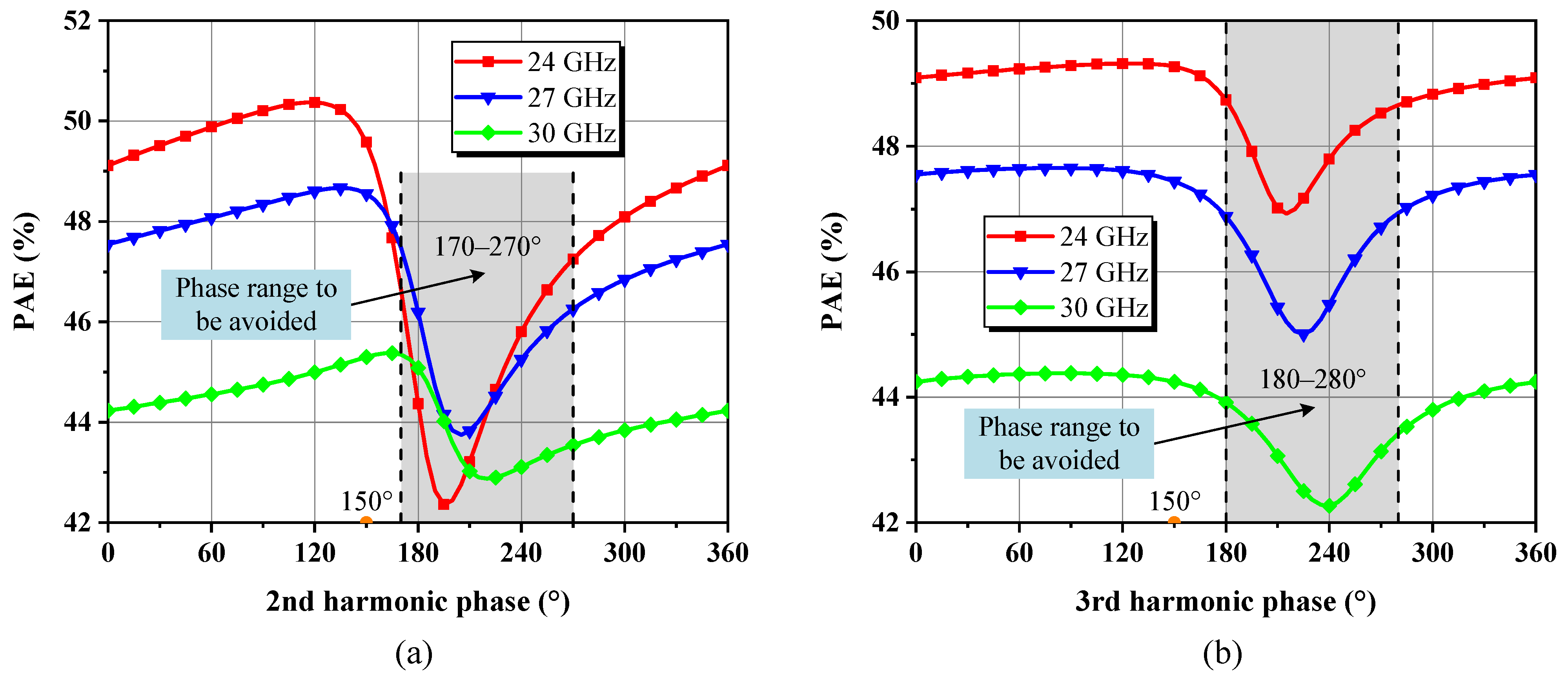
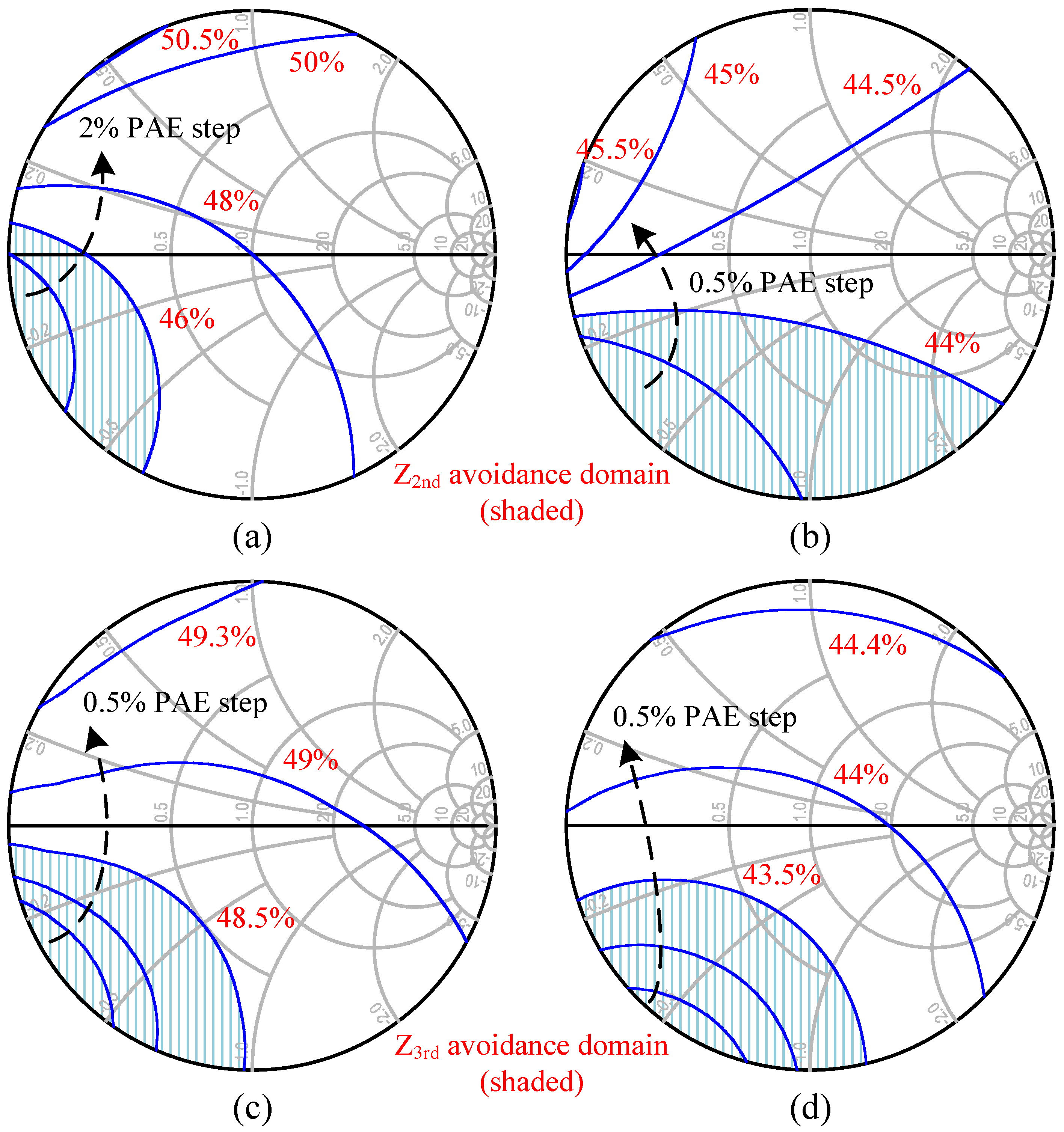
2.2. Harmonic Load-Pull Analysis and Determination of the Phase Avoidance Interval

According to energy conservation law, the total source power comprising the DC supply and the incident power Pin amounts to the Pout at fundamental and harmonic frequencies, plus the power dissipates into heat in the transistor, written as Equation (7). Harmonic impedances could be treated as almost purely reactive, i.e., the harmonic power contribution is modest, but they still act on the overlap of output V–I waveforms in the time domain, altering Pdiss. Thus, the second and third harmonic loads were varied one by one along the near periphery of the Smith chart, while keeping ZL,ctr at all fundamentals and the open circuit for other harmonic terminations to investigate the effect of their phase on the PAE of the 46 × 8 μm cell separately [14,24]. As seen from Figure 5a, the resulting PAE drops remarkably once the optimal phase is reached and curve families show deep notches in the 170–270° range, which indicates that the second harmonic termination leads to an increase in unwanted power dissipation when it is transformed into this phase interval. The peak-to-peak PAE reduction is about 8% to 3% from 24 GHz to 30 GHz. In contrast, except for a milder decline in the range of 180–280°, PAE curves in Figure 5b fluctuate little in the rest of the phase interval, which can be accepted as suitable ranges. These findings echo the earlier supposition that higher-order harmonics dampened by Cout lack enough strength to significantly affect the drain voltage waveform and thus are less effective against PAE. For most cases, only the first two-order harmonics deserve to be discussed. Manipulating more but minor harmonic objects in the broadband will multiply layout patterns and introduce higher losses than they are worth. Additionally, after repeating the present simulations at different gain compression points corresponding to Pin, we found that the phase ranges to be avoided converge, just with distinguishable differences in the degree of depression, and the deviation of the phase of the load reflection coefficient at the PAE valley due to Pin variations is less than 10° for each frequency. Figure 6 shows the detailed harmonic load-pull simulation results for PAE at 23 dBm of Pin.
P D C + P i n = P o u t + P d i s s = P o u t , f + n = 2 P o u t , n f + T v D S t i D t d t
In summary, the OMN design should strike a balance to prevent the harmonic impedances, especially the second one, from falling into the low-efficiency region. Fortunately, the wide tolerance range of 250° allows us to confidently concentrate on developing the fundamental MN, supplementing interventions with harmonic control, if necessary. The preferred phase location is considered between 0 and 150°.

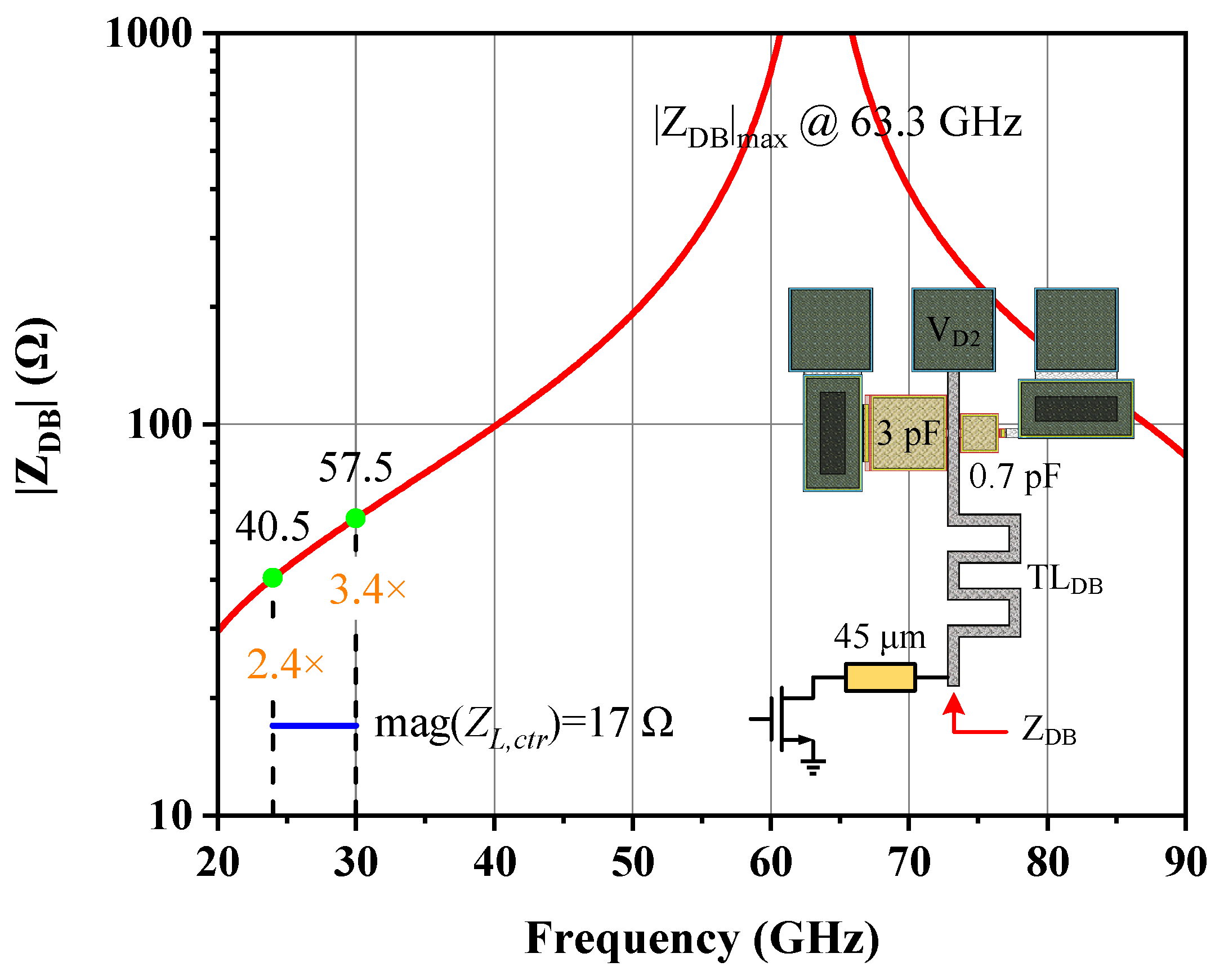
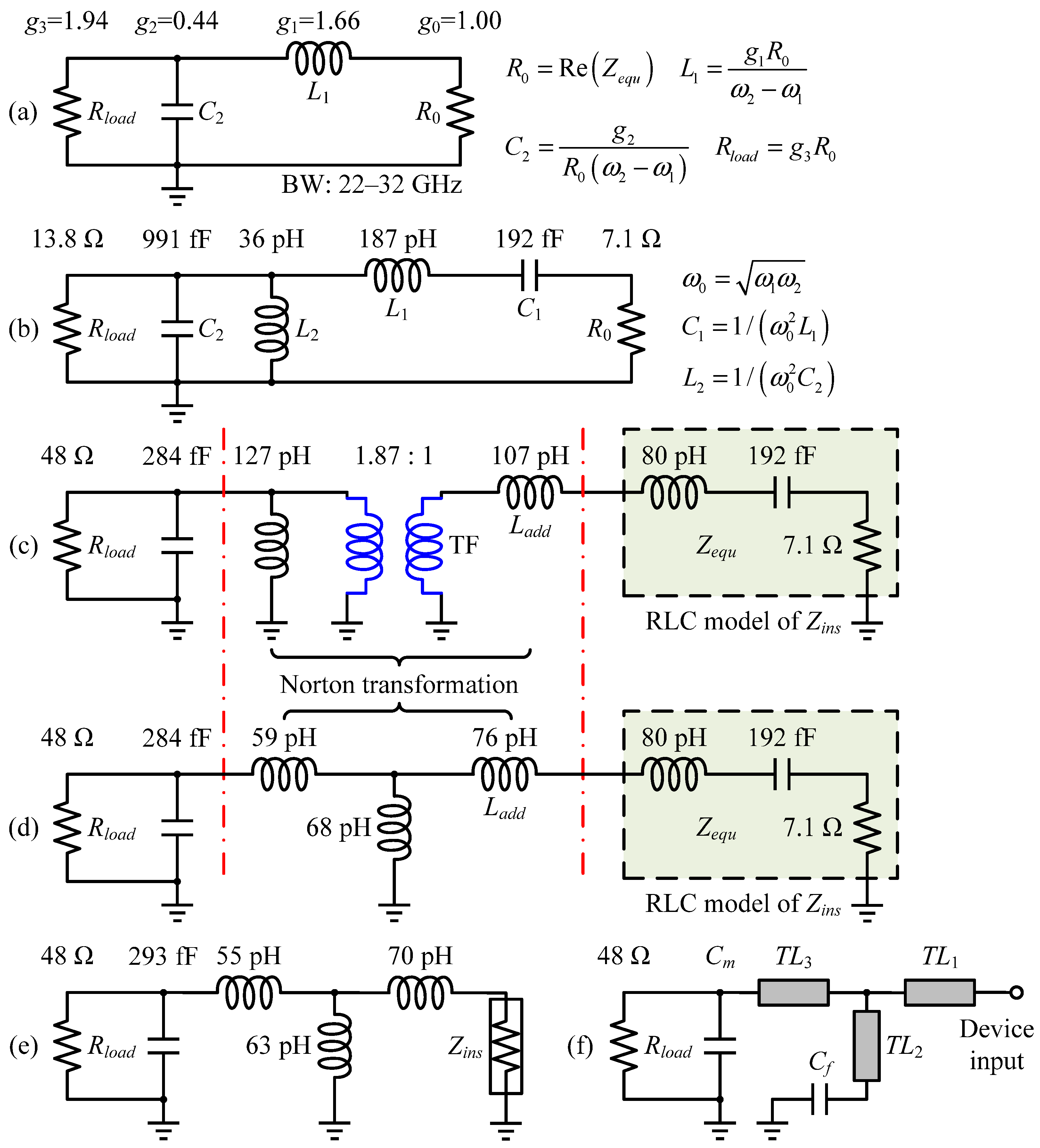
3. Design and Implementation of Matching Networks

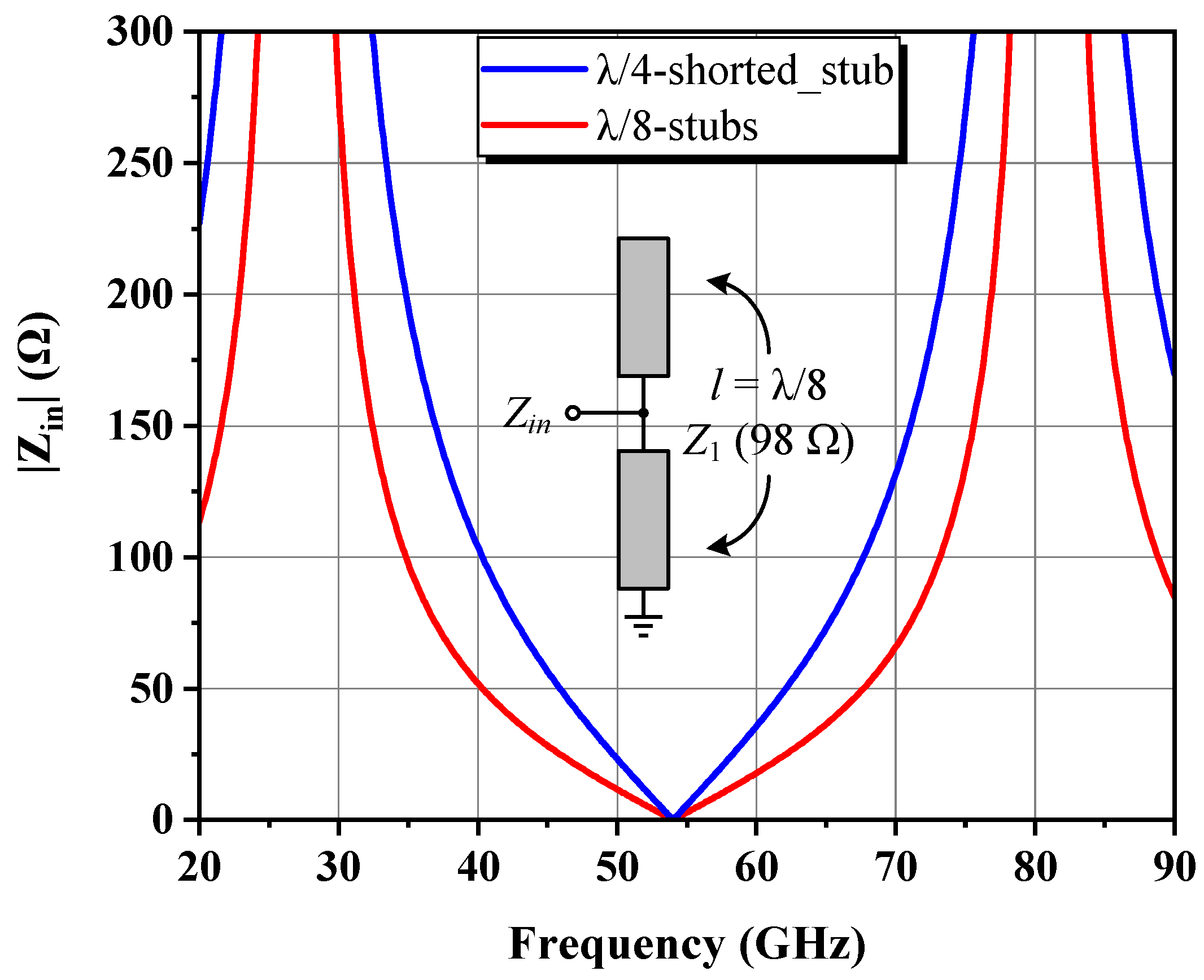
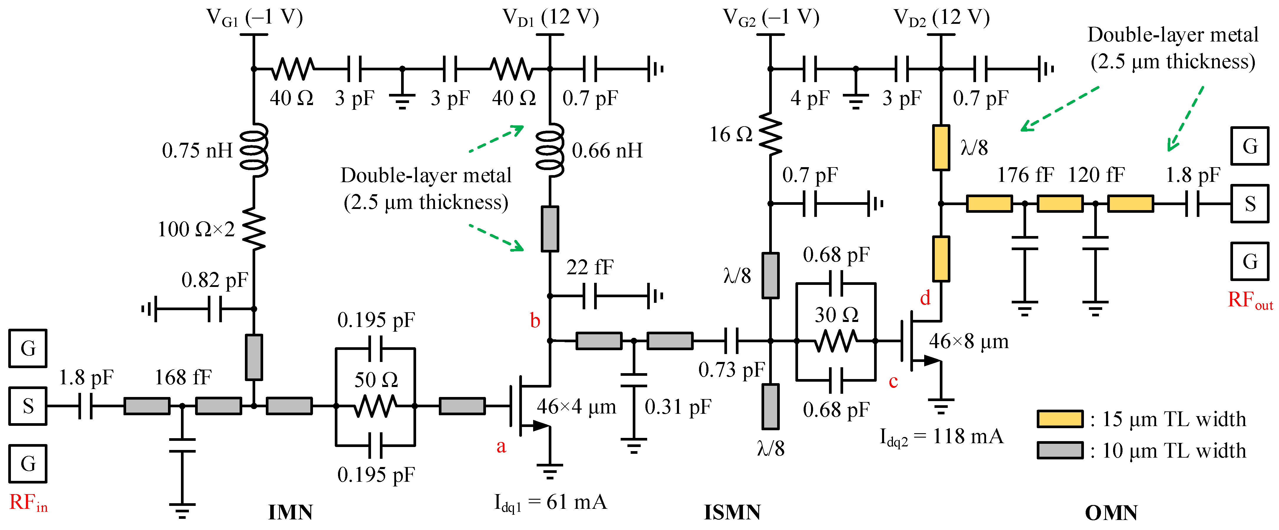
3.1. Mixed-Element Realization Method and Layout Considerations

Objectively speaking, in a manufactured MMIC, only some operable parameters of components can undergo limited unidirectional adjustment by physical trimming (e.g., laser), which requires sensible forethought and a well-planned setup during the design phase. The difficult-to-change nature implies that to accurately anticipate the real-world behavior of MMICs, especially for compact designs, we need rigorous electromagnetic (EM) simulations, which are time-consuming. When individually designed MNs and cells are cascaded into a complete amplifier following a generic modular implementation process, significant performance offsets tend to occur which are hard to eliminate. Each modification often involves performing thorough EM/circuit co-simulations to understand the corresponding knock-on effects, making it difficult to locate the root causes of problems or sensitive factors.
In view of the above facts, the schematic design alternated with layout replacement, continuously considering various EM influences throughout the development procedure, and the overall circuit was built in a step-by-step fashion to greatly reduce the difficulty and the number of optimization iterations in the final joint-tuning phase, ensuring that the desired results can be obtained efficiently.
For layout convenience and physical feasibility, MNs were constructed in a mixed-element style with microstrip lines and MIM capacitors. Generally, a section of transmission line with electrical length θ and characteristic impedance Z0 can be represented by a symmetric π-shaped network, described in Figure 7a. According to the definition of the Z-matrix, we have
Z T l i n e = j Z 0 cot θ j Z 0 csc θ j Z 0 csc θ j Z 0 cot θ
Z π = Z 1 Z 1 + Z 2 2 Z 1 + Z 2 Z 1 2 2 Z 1 + Z 2 Z 1 2 2 Z 1 + Z 2 Z 1 Z 1 + Z 2 2 Z 1 + Z 2
Letting Z|Tline = Z|π, gives
Z 1 = Z 0 j tan θ / 2 = 1 j B 1
Z 2 = j Z 0 sin θ = j X 2
For a transmission line segment whose physical length l is much smaller than the wavelength λ (l < λ/8), its equivalent parallel susceptance and series reactance are proximately linear to ω, that is
B 1 = tan θ / 2 Z 0 θ < 45 ° β l 2 Z 0 = ω l 2 v p Z 0 = ω C e q u
X 2 = Z 0 sin θ θ < 45 ° Z 0 β l = ω Z 0 l v p = ω L e q u
where vp is the phase velocity and β is the propagation constant. Therefore, the single-frequency equivalence technique illustrated in Figure 7b enables the approximate substitution of a series inductor with a distributed element [25]. Firstly, the obtained lumped prototype is decomposed into several cascaded subsections as needed, and one of the lossless units C1-L1-C2 is designated. Then, a prescribed symmetric π ladder with parallel capacitors Cequ centered on the inductor L1 is abstracted from its interior and replaced by a commensurate transmission line using the relations shown in Equations (12) and (13), with the chosen Z0 and in-band angular frequency ω0, where Lequ = L1, ω = ω0, and the C1 and C2 are deemed to be no less than Cequ. The termination capacitors CAn in the resulting mixed-element network are
C A n = C n C e q u = cos θ + ω 0 2 L 1 C n 1 ω 0 2 L 1   n = 1 , 2
In cases where the complete C1-L1-C2 combination cannot be divided, Equation (12) suggests that the remaining fringe capacitance Cequ can be reduced by selecting a larger Z0, hence decreasing the perturbation caused by unequal substitution on matching. Further, the narrow transmission line facilitates repeated bends to save the layout area, and as reflected by Equation (13), it also behaves more like an inductor. Thereby, small transmission line widths were chosen here. The line width was set to 10 μm with the exception of the OMN, where the line width was set to 15 μm. Supply routes and the OMN were deliberately thickened with double metal to diminish ohmic losses, enhancing the current handling capability for the former. In addition, 45° segments with perpendicular access lines were used at the corners to mitigate discontinuities and a gap of at least three times the line width was maintained between the adjacent matching microstrip lines to lower signal coupling. The 2.5D field simulator (Momentum) built into the Advanced Design System (ADS) software was used to solve all kinds of EM effects.

3.2. Synthesized Low-Pass OMN and ISMN

The Bode–Fano criterion clarifies the relationship between bandwidth Δω and the reflection coefficient Γ(ω). For the parallel RC-type load, the achievable lossless MN must comply with the constraint (Equation (15)), where Γm is the minimum return loss assumed to be constant over a certain frequency bandwidth ∆f. Ropt and Cout are now known to be 26 Ω and 0.27 pF, respectively, and with an ideal S11 of –25 dB, the theoretical limit ∆f can be calculated from the rearranged Equation (16) as 24.75 GHz, which is four times the actual demand. As a result, a large enough target simulation bandwidth BWsim could be chosen for the OMN, while maintaining a low passband ripple, yet this implies additional cost and insertion loss simultaneously. Bearing in mind the principle of miniaturization and design margin, the BWsim was set to be 22 to 32 GHz, a compromise, and the rest of the MN design would follow suit.
0 ln d ω Γ ω = Δ ω ln 1 Γ m π R o u t C o u t π R o p t 1 + R o p t G d s C d s + C g d π R o p t C o u t
Δ f = 1 2 R o p t C o u t ln 1 1 10 S 11 d B / 20
It is possible to have infinite ∆f with zero value capacitance, so properly handling Cout is the key to realizing a broadband OMN. There are two main ways: (1) tune existing matching elements or add specialized susceptance cancelation circuitry to minimize the effect of Cout [26,27], where passive negative susceptance networks, such as a compensating shunt inductor are preferable and more prevalent [23] and (2) absorb Cout into matching. Unfortunately, the Cout of 0.27 pF seems so large that neither compensation nor absorption appears to be a cost-effective or even a feasible option for on-chip wideband matching. To think otherwise, since ZL,ctr is the trade-off matching point for the entire target band, and not far from the real axis of the Smith chart, the OMN design can start with an impedance transformation from 48 Ω to real(ZL,ctr) and imag(ZL,ctr) is regarded as another sense of the quantity to be compensated. It should be noted that the L-shaped MN consisting of the parasitic shunt capacitor of the 100 μm square output pad and a 1.8 pF DC-block capacitor shifts the external 50 Ω load slightly down to the capacitive half-plane of the Smith chart, which was pulled back to 48 Ω at 27 GHz in advance by a high-impedance microstrip line. The RF input side received the same treatment.
A good OMN is one that is concise and easy to implement, with adequate harmonic suppression outside the band. According to the ITR, FBW, and passband ripple of 4, 0.4, and 0.1, respectively, a fourth-order Chebyshev low-pass filter was adopted as the matching prototype, where the normalized g value of each element was determined by lookup tables in [9] and then scaled to the 50 system and 27 GHz center frequency f0 to obtain the preliminary inductance and capacitance. Afterward, parameters of the acquired real-to-real network were automatically adjusted in the order of random-before-gradient type with the help of an ADS optimizer, which finally transformed the intermediate impedance of 12 Ω to the desired ZL,ctr [13]. Following the rules described in the preceding subsection to translate an OMN into a mixed-element form, a short-circuit stub TLDB was subsequently inserted as a drain bias branch, whose layout is displayed in Figure 8, along with the magnitude of its equivalent input impedance ZDB. The characterized open-circuit point lies at 63.3 GHz, somewhat higher than the second harmonic of the top fundamental frequency. Owing to the area limitation, the physical length of TLDB cannot be increased aggressively and the current equivalent effect of close to λ/8 makes the |ZDB| provided in the target band only 2.4–3.4 times larger than the |ZL,ctr|, which is well below the 100 Ω magnitude. Therefore, the OMN must be further optimized to minimize the disturbance to the original frequency response after integrating the indispensable TLDB. It is worth noting that the bias tee was intentionally placed 45 μm away from the transistor’s drain terminal, leaving this physical connection as a decoupling spacer to lessen the influence of the bias trace on the cell, which can only be presented with an established vendor model so that these inevitable EM interferences are not reflected in the simulation process.
Figure 9 shows how the response curve of the OMN rotates with the frequency inside the predefined optimal impedance domain and forms a knot signifying broadband matching, the junction of which corresponds to frequencies of 24 GHz and 31.5 GHz. Although the 22–32 GHz trajectory fails to sandwich ZL,ctr perfectly, it manages to fall into the narrow, preferred matching region as a whole, and the impedance at 32 GHz highly coincides with ZL,ctr, implying that the DA’s performance at the high-end fundamental is well secured and will not sharply deteriorate there. Furthermore, the second and third harmonic impedances exhibit relatively widespread scattering alongside the Smith chart’s margin, but neither are located in the aforementioned phase avoidance interval and therefore do not require extra harmonic manipulation.
The gate bias circuit of the output stage consists of open and shorted transmission lines with characteristic impedance Z1 (98 Ω for a single-layer metal microstrip that is 10 μm wide) and a length equal to λ/8 in parallel, as shown in Figure 10, whose input impedance Zin seen at the central node is expressed as Equation (17). Compared with the conventional quarter-wave short-circuit stub, the proposed structure not only serves the same function but also improves the layout flexibility, making full use of the free space on the top and bottom sides of the chip, and the extra multiplication factor of 0.5 helps to provide a better short-circuit termination state with extended bandwidth near the zeros, reducing even harmonic distortions from the front stage to be amplified together and mixed into the final product.
Z λ 8 s t u b s f = 1 2 j Z 1 tan π 2 f f f u n d = 1 2 Z λ 4 s h o r t e d _ s t u b
After loading the EM model of the well-developed OMN to the output stage cell, source-pull simulations were conducted where a series 0.73 pF DC-block capacitor was placed. The real and imaginary parts of the resulting in-band ZS,opt vary in a small range, from 4.4 to 5.2 Ω and from 5.3 to –4.4 Ω, respectively, so the task of the interstage matching network (ISMN) can be simply specified as a real impedance transformation from 5 to 75 Ω. It would be more economical and advantageous for the broadband by participating the entire transistor’s intrinsic output parasitic contribution into matching, rather than canceling out Cout through an inverse characteristic network or reoptimizing the finished real-to-real MN to compensate for it, which is important for the ISMN design that needs to cope with high ITR and simple requirements. Herein, a two-section Chebyshev impedance transformer centered at f0 was again adopted. Figure 11 illustrates a brief implementation flow of the ISMN for the lumped schematic phase, analogous to the OMN.

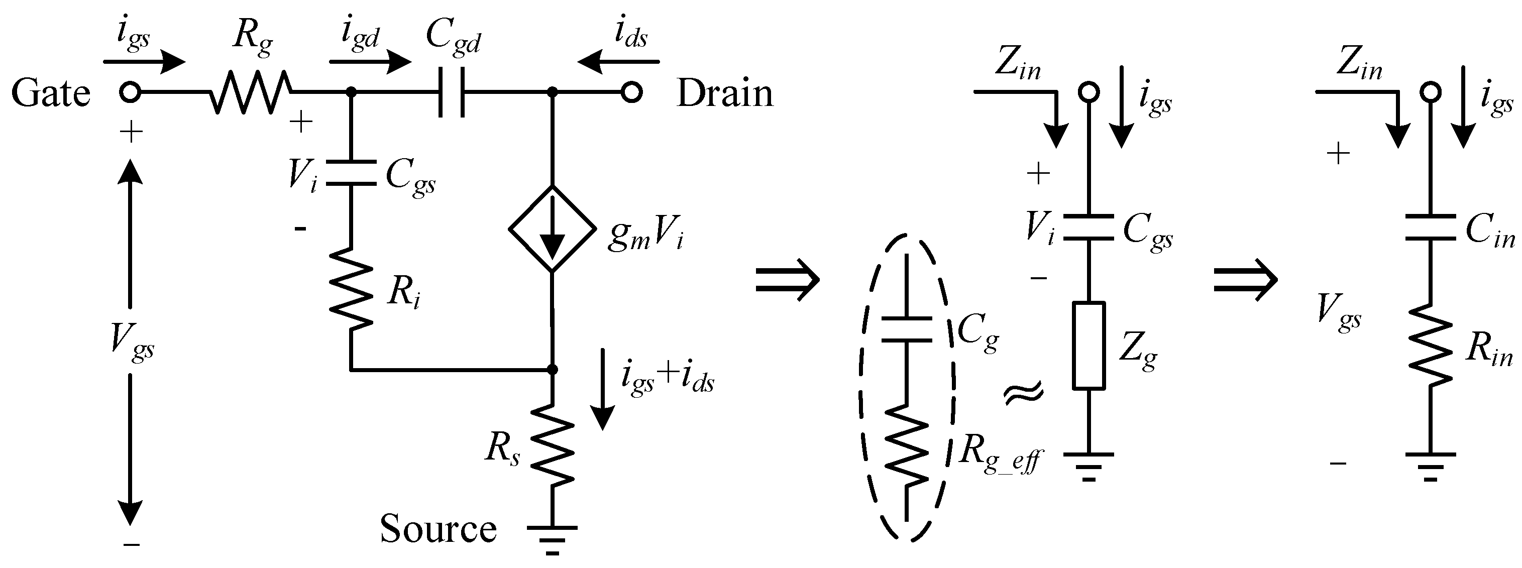
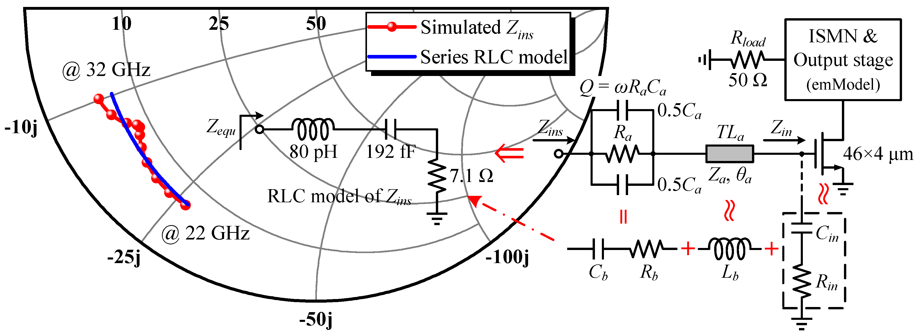
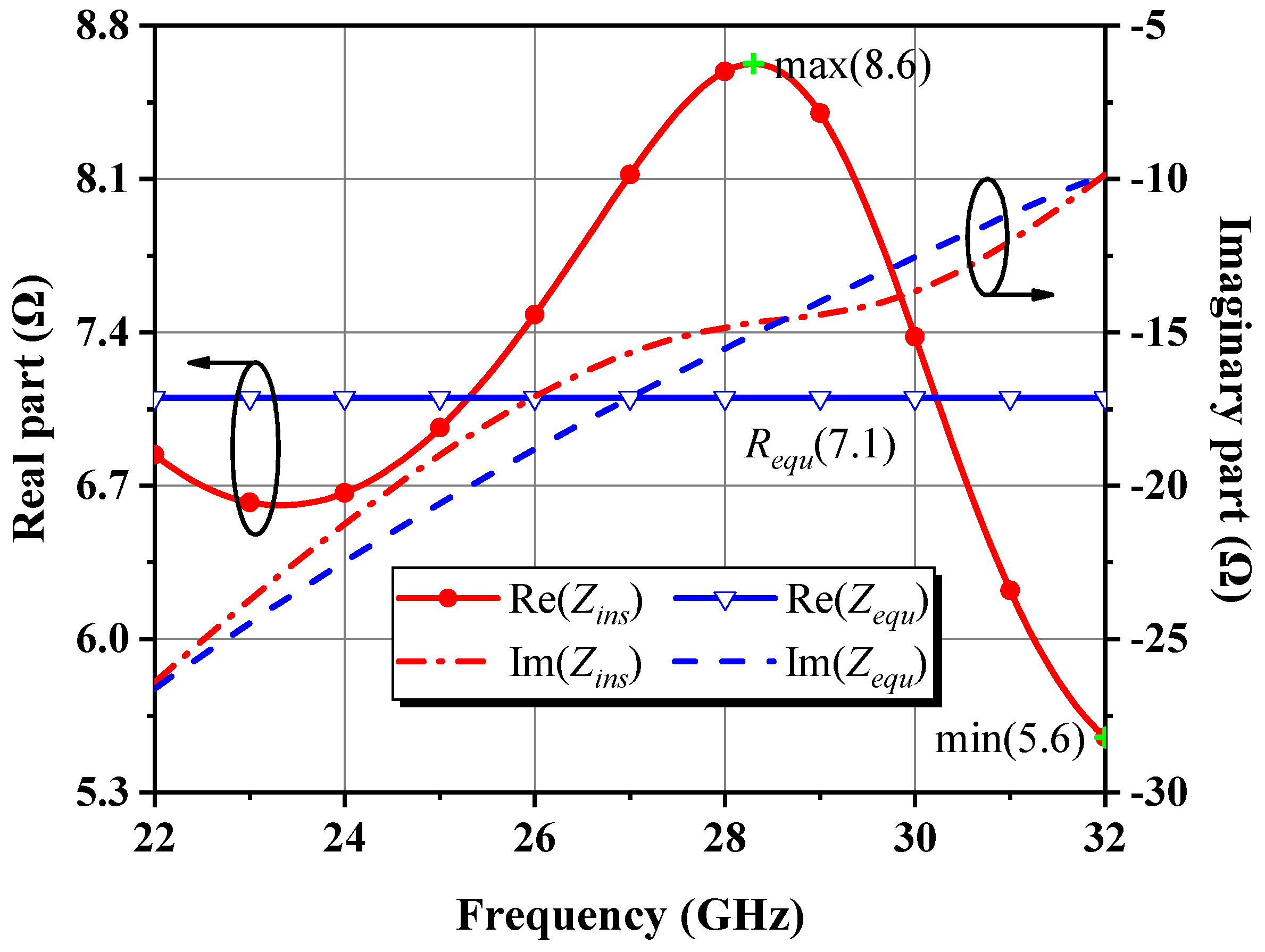
3.3. Input Impedance Model and the Synthesized Band-Pass IMN

The input matching network (IMN) is responsible for providing a complex conjugate match at the driver stage cell’s input in order to optimize gain flatness and achieve a nice input VSWR. Contrary to the output case, Zin seen from the gate of a GaN HEMT has a series RC nature, as demonstrated below. Referring to Figure 12 [28], applying Kirchhoff’s laws to the small-signal equivalent circuit of the HEMT input, the gate impedance Zg can be derived.
Z g = V g s V i i g s = R g + R i + R s + i d s i g s R s i g d i g s R i
Since igd is small and there exists igdigs, neglecting it for the sake of simplicity, we have
i d s i g s = g m V i i g d V i j ω C g s + i g d g m j ω C g s
Z g R g + R i + R s + g m R s j ω C g s = R g _ e f f + 1 j ω C g
where
C g = C g s g m R s
It is evident that Zg can be regarded as a series connection of an effective gate resistor Rg_eff formed by the sum of Rg, Ri, and Rs plus a capacitor Cg. Thus, Zin is expressed as
Z i n = Z g + 1 j ω C g s = R g _ e f f + 1 j ω C g s g m R s + 1 1 = R i n + 1 j ω C i n
Therefore, the impedance Zins seen at the new input node corresponds to a series RLC arrangement after the parallel RaCa stabilization network with a quality factor of Q and the connection line TLa are attached to the gate of the 46 × 4 μm cell loaded with all built-up post-stage circuits, expressed as Equation (23). It comprises a capacitor Cb and a resistor Rb resulting from the conversion of a parallel-to-series network, an inductor Lb approximating TLa, and Zin simplified as Rin in series with Cin, as illustrated in Figure 13, where the parameters of the equivalent RLC model fitted from simulations, and the agreement between its characterized impedance Zequ and Zins are also shown together. It is clear that the fit of the derived model is excellent at low frequencies in 22–32 GHz but declines to varying degrees as the frequency rises. Figure 14 reveals that this phenomenon is attributed to irregular changes in the real part of Zins, whose peaks and valleys occur at 28.3 GHz and 32 GHz, respectively, and the resistance in the model circuit was taken as their arithmetic mean value of 7.1 Ω. Though the imaginary parts of Zins and Zequ are closely matched within the 10 GHz bandwidth, there are no major undulating departures from each other, indicating that LC series resonance is the dominant form of Zins’s reactance, despite its complex behavior. The simulation results confirm the RLC model suggested by the theoretical analysis and the acceptability of the selected circuit parameters.
Z i n s R b + R i n + j ω L b + 1 j ω 1 C b + 1 C i n = R a Q 2 + 1 + R g _ e f f + j Z a sin θ a Q 2 ω C a Q 2 + 1 g m R s + 1 ω C g s
The dominant reactive constraint of the transistor input is a vital limiting factor for bandwidth extension, as is Cout. Thus, the optimal realization form of the broadband IMN will be the band-pass structure to absorb the extracted series resonant components. As a rule of thumb, higher-order filters are able to broaden the bandwidth and achieve steeper stopband attenuation, but we should be aware that a rise in order requires more elements to be employed, more time for EM optimization procedures, and will not offer linear improvement [11]. Another aspect to emphasize is that the band-pass network costs twice the same-order low-pass counterpart. On balance, the IMN was built as a second-order band-pass filter using closed-form solutions via mathematical derivations [10,14,15], and the detailed design steps are given in Figure 15. Because the RLC model is not entirely equivalent to Zins, the synthesized network must be fine-tuned for the actual frequency response before being converted into a mixed-element form, with the microstrip line TL2 serving as the gate bias path.
Given that the OMN is pivotal in deciding whether Pout and PAE objectives can be met, great efforts were undertaken early on and good outcomes were achieved. Hence, the joint-tuning phase solely entails adjusting the ISMN and the IMN. To enable a broadband gain response and input match, while maintaining favorable large-signal performance, concurrent small- and large-signal graded optimizations were carried out. The term “graded” refers to assigning more weight to optimization goals at the upper frequencies, which are an area of concern, so that a better fit gets produced sooner than with equal-weight settings.

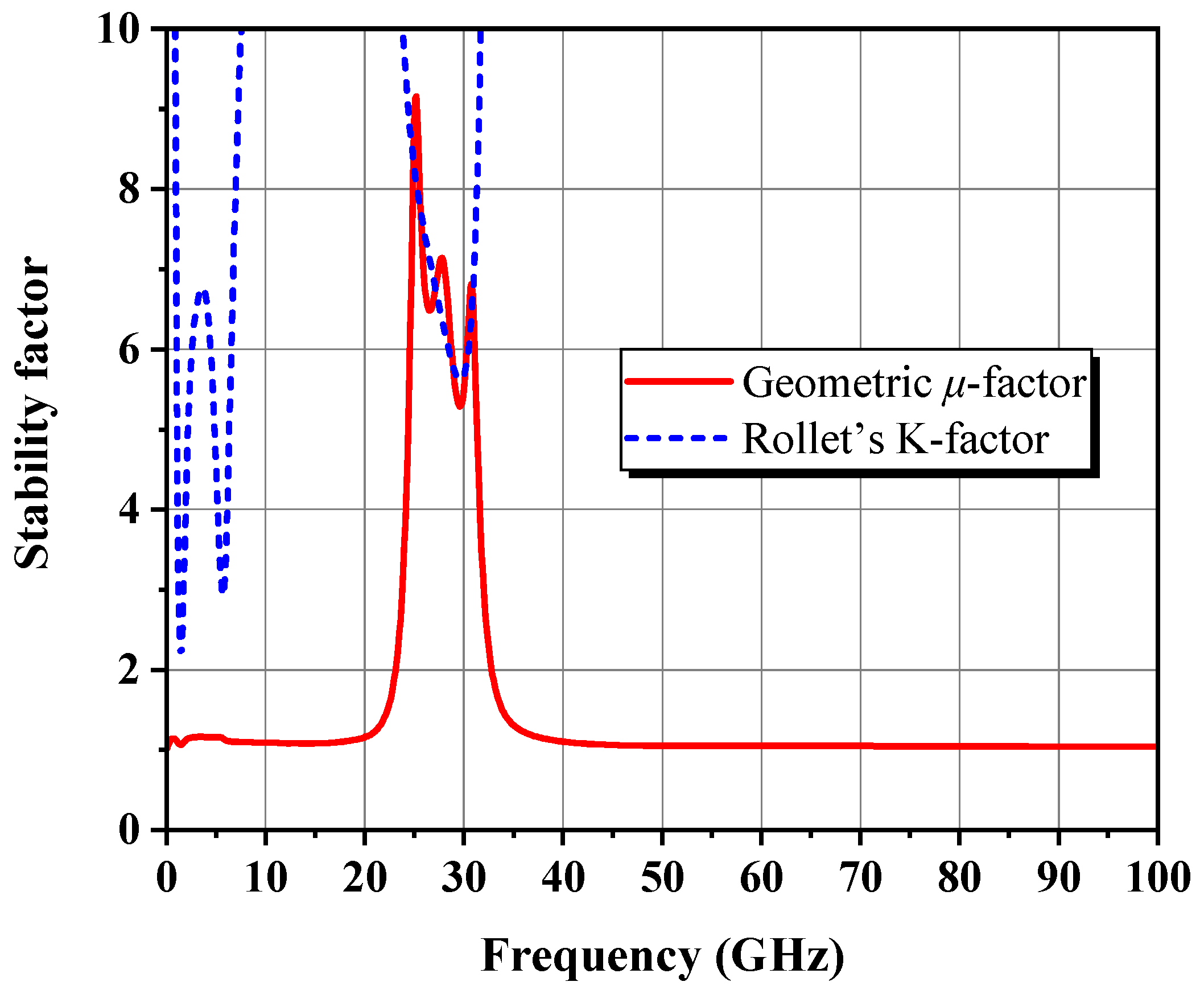
3.4. Loss Analysis of the MN and Stability of DA

Figure 16 depicts the entire circuit schematic, where the gate and drain feeds for each stage are provided independently, isolated from one another to eliminate interference and thus improve stability. To quantify the insertion loss (IL) associated with the MN, i.e., to calculate the difference between the power entering and leaving the MN as described in Equation (24), the DA was injected with a fixed low-power stimulus Pin away from the 1 dB gain compression point. Based on Figure 17 for an intuitive illustration, the six power sweep curves corresponding to various nodes indicated by the red labels in Figure 16 are linearly increasing in the interval of Pin less than 10 dBm, and the power difference between nodes in such class-A operation is nearly constant. Therefore, we read all node power with an arbitrary Pin of 4 dBm and obtained ILs of 0.78, 1.48, and 3.07 dB for the OMN, ISMN, and IMN at 28 GHz, respectively. When the RF output power is progressively saturated, the curve Pc displays a quasi-proportional growth trend mildly deviating from linearity, which denotes that the front stage neither works in the deep back-off region of low efficiency nor demonstrates insufficient driving power, avoiding unnecessary DC consumption and distortion generation. As a consequence, the bias Q-point and the staging ratio of 1:2 settings were verified to be appropriate to some extent. Likewise, the overall frequency responses shown in Figure 18 can be obtained. To achieve the highest possible PAE in the context of compactness, the OMN was implemented in a simple structure and used high characteristic impedance microstrip lines with a double-layer metal, whose maximum IL does not exceed 0.9 dB over 24–30 GHz. In contrast, the IL trend of the ISMN and the IMN compensates well for the device’s negative gain roll-off slope, with the IMN being the main contributor, which reveals the reason for its large low-frequency loss. The total IL of three MNs is regulated within 9.23 dB in the designed band and exhibits a trend of rapidly decreasing with increasing frequency and then leveling off and steadily growing, with the valley at 28 GHz, corresponding to a minimum value of 5.33 dB.
IL = P i n _ M N P o u t _ M N
Apart from the inherent dissipation loss of the MN, another is the mismatch loss, which together ensures the gain flatness of the DA. The total efficiency ηtol of a lossy MN is defined as the ratio of the delivered power PL (i.e., Pout_MN) absorbed by load to the available power Pavs from the source Vg, expressed as
η t o l = P L P a v s = P i n _ M N P a v s × P o u t _ M N P i n _ M N = η m a t c h × η l o s s
where ηloss is the MN’s transmission efficiency, which equals 1 in the absence of the MN. The matching efficiency ηmatch can be further derived as Equation (26), which equals 1 in the case of conjugate matching, where ZS = RS + jXS is the source impedance and Zin = Rin + jXin is the input impedance of the MN with a load attached. Table 3 details the simulated ηmatch and ηloss for all MNs in the range of 23–31 GHz, and their product ηtol is plotted in Figure 19. These findings validate the effectiveness of the filter synthesis theory in creating broadband MNs and explicitly reflect the design focus of each MN. The OMN scores well among various efficiency indicators, where the in-band ηtol surpasses 77.2% and fluctuates no more than 5.4%, ensuring a smooth and low-loss power transfer. As for the ISMN, ηmatch shows a more prominent trend of increasing with frequency than ηloss, with the difference between the highest and lowest fundamental frequencies of ηmatch being up to 27.2%, which represents the broadband strategy implemented by the ISMN to better match at the high-frequency side and introduce a proper low-frequency mismatch to cope with the demanded driving power of the output stage growing with frequency. In addition, ηloss remains above 59.2%, so the adverse impact of the associated IL on gain and PAE is still tolerable. Thanks to the applied band-pass filter structure, the IMN manifests superior and nearly uniform ηmatch. Nonetheless, we intentionally sacrifice ηloss to attain an eventual broadband gain response with enhanced stability in return for losing more than half of the transmitted signal energy, which seldom compromises large-signal performance. Overall, they exhibit a gradient decreasing ηtol from the OMN to the IMN, with peaks lying in the upper-frequency portion (28–30 GHz).
η m a t c h = P i n _ M N P a v s = V g R S + R i n + j X S + X i n 2 R i n V g 2 4 R S = 4 R i n R S Z i n + Z S 2
Before tape-out, it is mandatory to carefully check the overall stability of the DA. To ensure that the DA is unconditionally stable under any possible operating conditions, countermeasures were incorporated into the design by (1) connecting a parallel RC network in front of the two transistors, (2) inserting a resistor in both gate bias paths, (3) paralleling a series combination of a 3 pF bypass capacitor and a 40 Ω resistor to the gate and drain supply lines of the driver stage, and (4) in conjunction with the resistive losses of all MNs. Figure 20 proves that the simulated stability factors μ and K are greater than unity over DC–100 GHz.

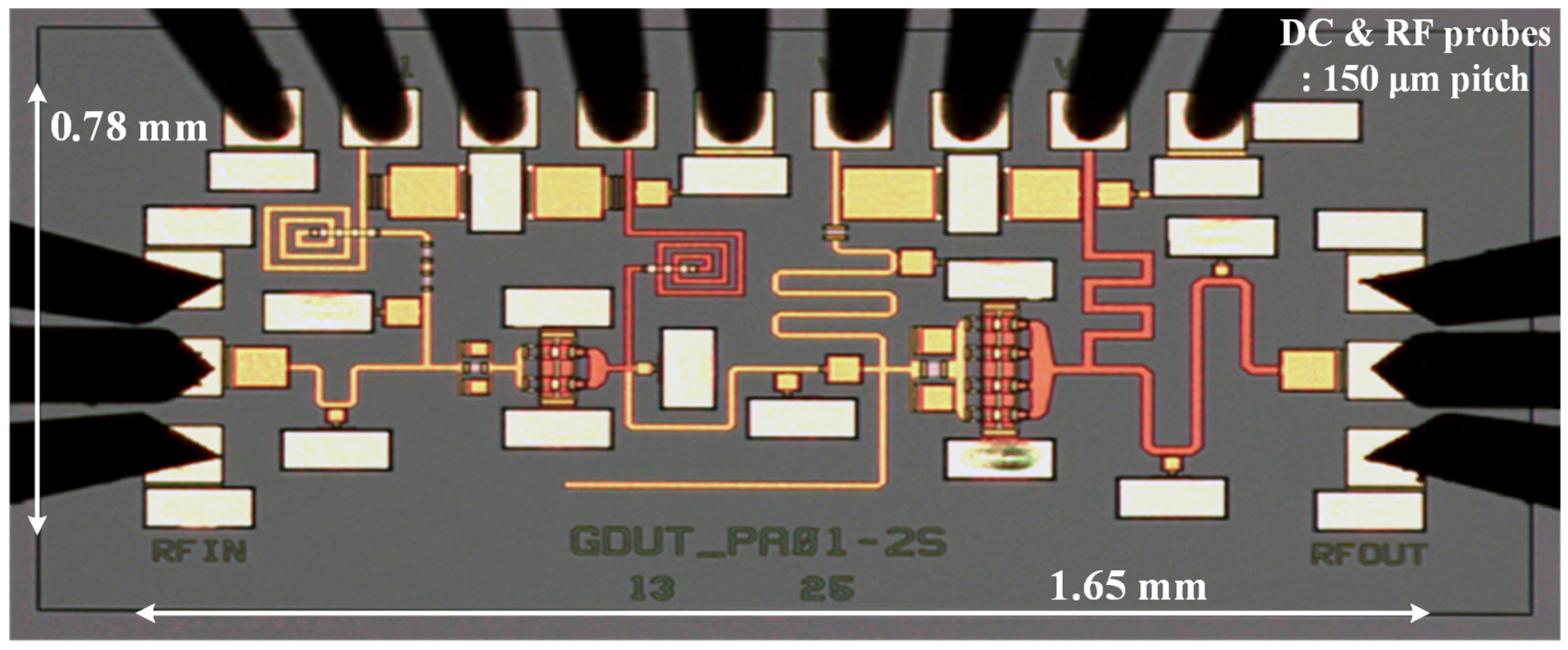
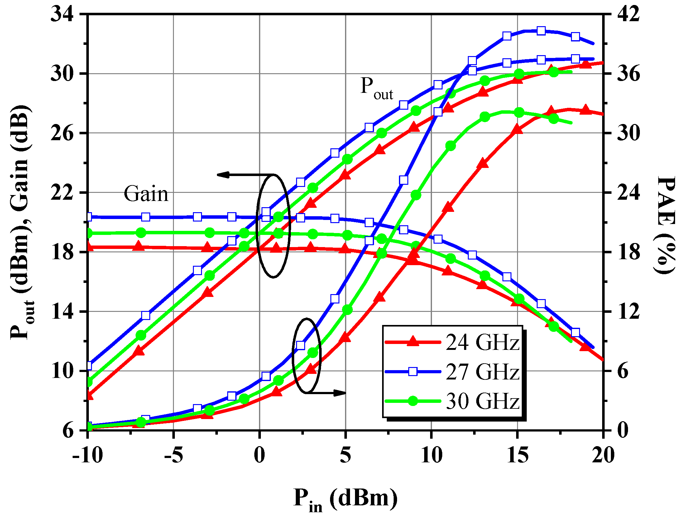
4. Probed Measurement Results

Instead of assembling the bare die into a fixture to avoid bonding inductive interconnected gold wires to the RF pads and causing uncertainty in the original impedance matching, we conducted on-wafer testing of the fabricated MMIC DA using ground–signal–ground (GSG) microwave probes and dedicated DC probe cards for proper DC decoupling with a manually-controlled probe station. Figure 21 shows a close-up micrograph where tapers were added that fit with the device drain pin width to reduce step junction discontinuities. However, the thermal contact between the backside of the chip and the heat sink surface will be poor and lead to inferior heat dissipation [22], which may provoke thermal degradation or even burnout of the transistor. To prevent overheating, a 12 V pulsed supply with a 5% duty cycle (200 μs pulse width and 4 ms period) was applied. First, performing necessary but quick partial stability inspections, the gate bias voltage was slowly raised from the threshold of –1.5 V to bring the quiescent current draw of the DA to 179 mA, in line with the simulation environment in the absence and presence of weak sinusoidal excitation, with no oscillations monitored across the full spectrum during both processes. Afterward, a series of measurements were carried out at room temperature using the N5183A MXG analog signal generator, N5245A PNA-X network analyzer, and N9021B MXA signal analyzer from Keysight (Santa Rosa, CA, USA).

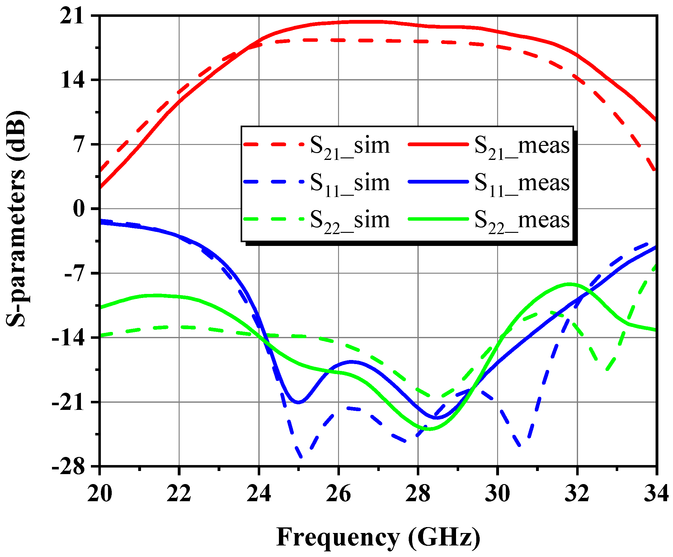
4.1. Small-Signal Characterization

Figure 22 exhibits that S21 ranges between 18.3 and 20.3 dB within the 24–30 GHz operating bandwidth, which is higher than predicted in the CW mode from 24 GHz onward, with an average in-band excess of about 1.7 dB. Simulated S11 gives a distinct band-pass Chebyshev equal-ripple response, whereas S22 is relatively poor, as described from the conceptual standpoint that the output stage is power matching via load-pull instead of small-signal conjugate matching, so the S22 performance is sacrificed at some expense in exchange for enhanced Pout. Their respective in-band measured values stay below –12 dB and –13.9 dB, suggesting that the input/output ports are well matched.

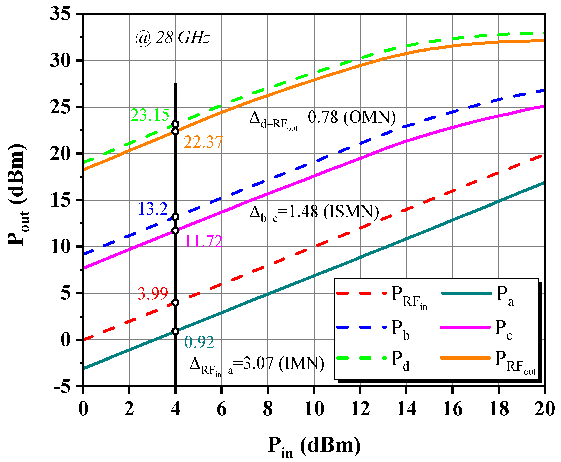
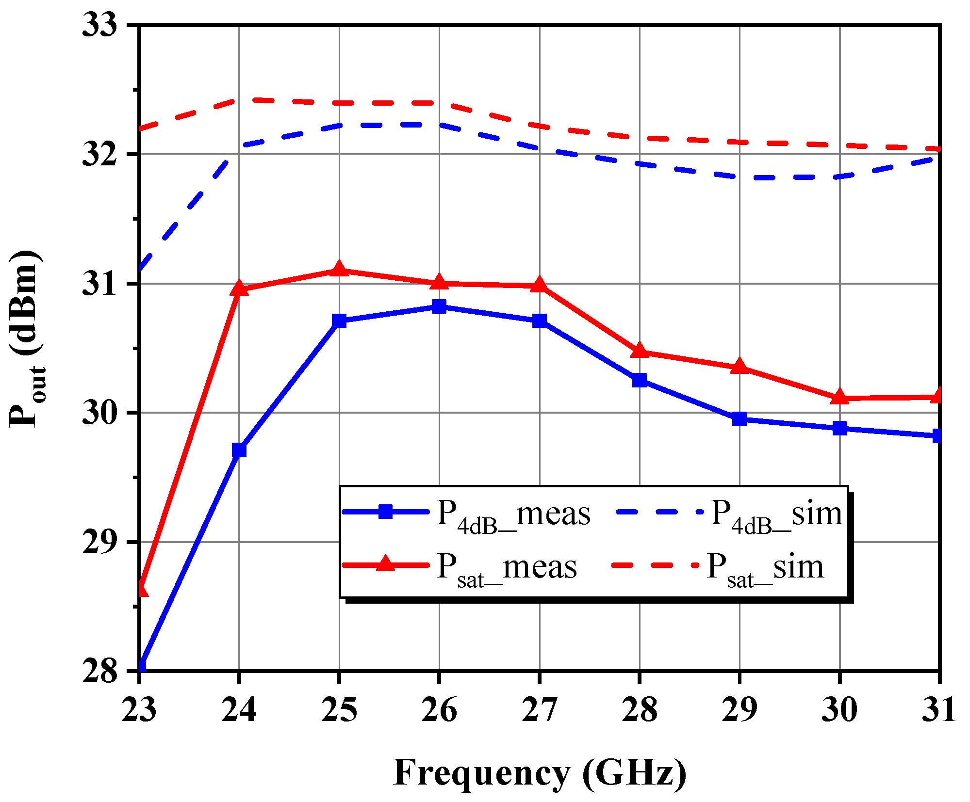
4.2. Large-Signal Characterization

A close examination of Figure 23 and Figure 24 reveals that the collected P4dB and Psat over the band of interest are 29.7–30.8 dBm and 30.1–31.1 dBm, respectively, following almost the same trend as expected, with only an overall decline of about 1.7 dB and 1.5 dB from their simulated counterparts. The PAE at P4dB exceeds 30.9% in the band, with a peak of 39.8% at f0, and the curve is displaced by 1 GHz to higher frequencies compared to the simulation. Figure 25 depicts power sweep curves at low, medium, and high fundamentals, which show that the DA characterizes the anticipated soft compression behavior, generally reaching the critical saturation state in the vicinity of P6dB, but more boost power is required for the low-frequency case. This might be because of nonlinear trapping effects, which are more pronounced in GaN-on-Si than GaN-on-SiC, as the former has a higher defect density. In addition, the highest PAE occurs at about 2 dB back from the saturation point and total current consumption grows to 241–283 mA when the DA is driven into the 8 dB gain compression state. No case of instability was detected throughout the tests. Therefore, the applied stability measures seem to be sufficient.
The measured and simulated outcomes agree well in terms of trends, but they differ somewhat in data values and also partly show slight frequency deviations, which are mainly attributed to: the accuracy of the transistor modeling; inevitable and stochastic manufacturing errors, especially in MIM capacitors; channel temperature variations due to self-heating from gate finger dissipation; the calibration status of the entire test system; and the contact quality between the probes and RF pads. Note that the nonlinear scalable model of the device provided by the foundry was established on the basis of the measurement of typical test kits, and the ones with specific sizes used here were extrapolated through mathematical fitting from several validated samples. Therefore, they may not accomplish the same high accuracy as typical cells. Table 4 summarizes the experimental results in comparison to previously reported PAs with similar frequency bands.

5. Conclusions

This paper demonstrates a fully integrated 1-watt GaN MMIC DA for the 24–30 GHz band. The optimal impedance domain with a moderate range was delineated through simplified load-pull simulations according to reasonably preset goals. The reference center impedance ZL,ctr was calculated by weighted averaging, with an emphasis on high-frequency PAE. As per the proposed target space consisting of an area and a single point instead of discrete compromise matching points at different fundamental frequencies or arcs formed by theoretical impedance sets, as in class-J amplifiers, the implementation process avoids addressing the tricky impedance-tracking problem and relieves the pressure of broadband design. The low-loss OMN without harmonic control circuitry was thereafter developed applying the Chebyshev filter synthesis theory and paired with CAD post-optimization to ensure that the transformed in-band impedance trajectory nestles inside the preferred region, which can better solve the contradiction between multiple metrics under a broadband. With the same fourth-order low-pass ladder based on a Chebyshev response, the ISMN differs from the OMN in that it exploits the transistor’s Cout de-embedded from load-pull contours to complete the compact broadband matching at an ITR as high as 15. For the series RLC model established by theoretical analysis and simulation, equivalent to the stabilized cell’s input impedance, the IMN was realized as a band-pass filter using closed-form solutions to absorb the resonant input parasitics, achieving a return loss of 12 dB minimum in the 6 GHz bandwidth. The step-by-step circuit construction strategy rather than direct modular assembly allows the remaining MNs to be designed on the basis of frequency responses from a progressively built and refined EM model, which lessens the risk of unmitigated performance deviations or laborious adjustments during the joint-tuning phase, thus increasing the design efficiency and success rate. Moreover, this is greatly beneficial for amplifiers with larger-scale architectures, such as N-way combining and differential, as the reduction in simulation time is more significant than with conventional ways. The answers provided in this work in tackling broadband problems were outlined in terms of analyzing the losses of each MN, and experimental results validate the proposed design scheme. The realized two-stage DA has a linear gain of 19.3 dB on average, with a less than 1 dB fluctuation in the operating bandwidth and a state-of-the-art PAE of up to 39.8%, with tight integration and a small size of 1.29 mm2, contributing to lower fabrication and production costs, all of which prove the suitability of the presented design for massive commercial 5G mmW applications.

Author Contributions

Conceptualization, L.P.; methodology, L.P.; software, L.P.; validation, L.P.; formal analysis, L.P.; investigation, L.P.; data curation, L.P. and J.Y.; writing—original draft preparation, L.P.; writing—review and editing, L.P. and Z.Z.; visualization, L.P.; supervision, G.Z.; project administration, Z.Z. and G.Z.; funding acquisition, G.Z. All authors have read and agreed to the published version of the manuscript.

Funding

This research was funded by the National Key R&D Program of China, grant number 2018YFB1802100, and the National Natural Science Foundation of China, grant number 61974035.

Institutional Review Board Statement

Not applicable.

Informed Consent Statement

Not applicable.

Data Availability Statement

Not applicable.

Acknowledgments

The authors thank the staff of Sichuan YiFeng Electronic Science and Technology Co., Ltd., for their support during the testing phase.

Conflicts of Interest

The authors declare no conflict of interest.

References

  1. Camarchia, V.; Quaglia, R.; Piacibello, A.; Nguyen, D.P.; Wang, H.; Pham, A.V. A review of technologies and design techniques of millimeter-wave power amplifiers. IEEE Trans. Microw. Theory Tech. 2020, 68, 2957–2983. [Google Scholar] [CrossRef]
  2. Peng, L.; Li, J.; Zhang, G.; Lin, S.; Chen, J. Ka-band GaAs MMIC driver amplifier design. In Proceedings of the 2020 IEEE 3rd International Conference on Electronic Information and Communication Technology (ICEICT), Shenzhen, China, 13–15 November 2020; pp. 287–290. [Google Scholar]
  3. Li, T.W.; Huang, M.Y.; Wang, H. Millimeter-wave continuous-mode power amplifier for 5G MIMO applications. IEEE Trans. Microw. Theory Tech. 2019, 67, 3088–3098. [Google Scholar] [CrossRef]
  4. Cripps, S.C. RF Power Amplifiers for Wireless Communications, 2nd ed.; Artech House: Norwood, MA, USA, 2006. [Google Scholar]
  5. Cripps, S.C.; Tasker, P.J.; Clarke, A.L.; Lees, J.; Benedikt, J. On the continuity of high efficiency modes in linear RF power amplifiers. IEEE Microw. Wirel. Compon. Lett. 2009, 19, 665–667. [Google Scholar] [CrossRef]
  6. Yarman, B.S.; Carlin, H.J. A simplified “real frequency” technique applied to broad-band multistage microwave amplifiers. IEEE Trans. Microw. Theory Tech. 1982, 30, 2216–2222. [Google Scholar] [CrossRef]
  7. An, J.; Song, K.; Zhang, S.; Yang, J.; Cao, P. Design of a broadband electrical impedance matching network for piezoelectric ultrasound transducers based on a genetic algorithm. Sensors 2014, 14, 6828–6843. [Google Scholar] [CrossRef] [PubMed] [Green Version]
  8. Zhang, J.-L.; Wang, H.-Z.; Zheng, Z.-Q.; Zhu, X.-Z. Research of SRFT improving and antenna broadband matching based on the IWO–LM algorithm. IET Microw. Antennas Propag. 2018, 12, 2320–2325. [Google Scholar]
  9. Matthaei, G.L. Tables of Chebyshev impedance–transforming networks of low-pass filter form. Proc. IEEE 1964, 52, 939–963. [Google Scholar] [CrossRef] [Green Version]
  10. Dawson, D.E. Closed-form solutions for the design of optimum matching networks. IEEE Trans. Microw. Theory Tech. 2008, 57, 121–129. [Google Scholar] [CrossRef]
  11. Meng, X.; Yu, C.; Liu, Y.; Wu, Y. Design approach for implementation of class-J broadband power amplifiers using synthesized band-pass and low-pass matching topology. IEEE Trans. Microw. Theory Tech. 2017, 65, 4984–4996. [Google Scholar] [CrossRef]
  12. Nakatani, K.; Yamaguchi, Y.; Hangai, M.; Shinjo, S. A Ka-band CW 15.5 W 15.6% fractional bandwidth GaN power amplifier MMIC using wideband BPF inter-stage matching network. In Proceedings of the 2019 IEEE BiCMOS and Compound Semiconductor Integrated Circuits and Technology Symposium (BCICTS), Nashville, TN, USA, 3–6 November 2019; pp. 1–4. [Google Scholar]
  13. Chen, K.; Peroulis, D. Design of highly efficient broadband class-E power amplifier using synthesized low-pass matching networks. IEEE Trans. Microw. Theory Tech. 2011, 59, 3162–3173. [Google Scholar] [CrossRef]
  14. Saad, P.; Fager, C.; Cao, H.; Zirath, H.; Andersson, K. Design of a highly efficient 2–4-GHz octave bandwidth GaN-HEMT power amplifier. IEEE Trans. Microw. Theory Tech. 2010, 58, 1677–1685. [Google Scholar] [CrossRef]
  15. Feuerschütz, P.; Friesicke, C.; Quay, R.; Jacob, A.F. A Q-band power amplifier MMIC using 100 nm AlGaN/GaN HEMT. In Proceedings of the 2016 11th European Microwave Integrated Circuits Conference (EuMIC), London, UK, 3–4 October 2016; pp. 305–308. [Google Scholar]
  16. Yang, M.; Xia, J.; Guo, Y.; Zhu, A. Highly efficient broadband continuous inverse class-F power amplifier design using modified elliptic low-pass filtering matching network. IEEE Trans. Microw. Theory Tech. 2016, 64, 1515–1525. [Google Scholar] [CrossRef] [Green Version]
  17. Peng, L.; Chen, J.; Zhang, Z.; Huang, Y.; Wang, T.; Zhang, G. Design of broadband high-gain GaN MMIC power amplifier based on reactive/resistive matching and feedback technique. IEICE Electron. Express 2021, 18, 20210313. [Google Scholar] [CrossRef]
  18. Neininger, P.; John, L.; Brückner, P.; Friesicke, C.; Quay, R.; Zwick, T. Design, analysis and evaluation of a broadband high-power amplifier for Ka-band frequencies. In Proceedings of the 2019 IEEE MTT-S International Microwave Symposium (IMS), Boston, MA, USA, 2–7 June 2019; pp. 564–567. [Google Scholar]
  19. Chen, S.; Nayak, S.; Campbell, C.; Reese, E. High efficiency 5W/10W 32-38GHz power amplifier MMICs utilizing advanced 0.15 µm GaN HEMT technology. In Proceedings of the 2016 IEEE Compound Semiconductor Integrated Circuit Symposium (CSICS), Austin, TX, USA, 23–26 October 2016; pp. 1–4. [Google Scholar]
  20. Tong, X.; Zhang, S.; Zheng, P.; Xu, J.; Wang, R. 23.5–30 GHz gallium nitride on silicon power amplifier MMIC with 7.6–12.4 W saturation output power. Microw. Opt. Technol. Lett. 2019, 61, 1797–1801. [Google Scholar] [CrossRef]
  21. OMMIC. U-GaN Design Manual v1.3.1; OMMIC: Limeil-Brévannes, France, 2020. [Google Scholar]
  22. Moron, J.; Leblanc, R.; Lecourt, F.; Frijlink, P. 12W, 30% PAE, 40 GHz power amplifier MMIC using a commercially available GaN/Si process. In Proceedings of the 2018 IEEE/MTT-S International Microwave Symposium-IMS, Philadelphia, PA, USA, 10–15 June 2018; pp. 1457–1460. [Google Scholar]
  23. Lee, W.; Kang, H.; Lee, H.; Lim, W.; Bae, J.; Koo, H.; Yoon, J.; Hwang, K.C.; Lee, K.Y.; Yang, Y. Broadband InGaP/GaAs HBT power amplifier integrated circuit using cascode structure and optimized shunt inductor. IEEE Trans. Microw. Theory Tech. 2019, 67, 5090–5100. [Google Scholar] [CrossRef]
  24. Tu, Z.; Li, B.; Shang, Y.; Wang, Z.; Wang, L.; Liu, D.; Zhou, M.; Huang, Z.; Yu, F. High-efficiency K-band MMIC power amplifier using multi-harmonic load terminations. Microelectron. J. 2015, 46, 1453–1458. [Google Scholar] [CrossRef]
  25. Yarman, B.S.; Aksen, A. An integrated design tool to construct lossless matching networks with mixed lumped and distributed elements. IEEE Trans. Circuits Syst. I Fundam. Theory Appl. 1992, 39, 713–723. [Google Scholar] [CrossRef]
  26. Rubio, J.J.M.; Quaglia, R.; Piacibello, A.; Camarchia, V.; Tasker, P.J.; Cripps, S. 3–20-GHz GaN MMIC Power Amplifier Design Through a COUT Compensation Strategy. IEEE Microw. Wirel. Compon. Lett. 2021, 31, 469–472. [Google Scholar] [CrossRef]
  27. Ardekani, M.H.M.; Abiri, H. A new approach to design wide band power amplifiers by compensating parasitic elements of transistors. AEU-Int. J. Electron. Commun. 2018, 92, 1–7. [Google Scholar] [CrossRef]
  28. Dennler, P. Analysis of the Potential of Gallium Nitride Based Monolithic Power Amplifiers in the Microwave Domain with More than an Octave Bandwidth. Ph.D. Thesis, Albert-Ludwigs-Universität Freiburg, Breisgau, Germany, 2014. [Google Scholar]
  29. Qorvo. High Frequency Amplifiers, TGA2594 Data Sheet. Available online: http://www.qorvo.com (accessed on 11 November 2022).
Figure 1. (a) Epitaxial structure and (b) cross-section of OMMIC’s 0.1 μm GaN-on-Si process.
Micromachines 14 00175 g001
Figure 2. Simulated load-pull contours at 1 dB gain compression and the GP circle of 8 dB at 30 GHz for the output stage cell when given a nominal bias point of VD = 12 V and VG = –1 V, which yields the maximum device DC and AC transconductance [17].
Micromachines 14 00175 g002
Figure 3. Preferred region in the optimal impedance domain.
Micromachines 14 00175 g003
Figure 4. Equivalent parallel RC model for the large-signal output impedance of an HEMT.
Micromachines 14 00175 g004
Figure 5. Influence of the (a) second and (b) third harmonic phases on simulated PAE at different frequencies for a constant 0.95 magnitude of load reflection coefficient when given 23 dBm of available Pin.
Micromachines 14 00175 g005
Figure 6. Harmonic load-pull simulation results: second harmonic at (a) 24 GHz and (b) 30 GHz; third harmonic at (c) 24 GHz and (d) 30 GHz.
Micromachines 14 00175 g006
Figure 7. (a) Equivalent two-port network of a transmission line. (b) Swap an identified lumped low-pass π-section into its almost equivalent mixed-element counterpart using the replacement technique.
Micromachines 14 00175 g007
Figure 8. Drain bias network used in the output stage and its equivalent input impedance.
Micromachines 14 00175 g008
Figure 9. EM-simulated transformation feature (S11) of the OMN from 22 to 90 GHz.
Micromachines 14 00175 g009
Figure 10. Impedance response of the ideal suggested even harmonic trap circuit designed at f0 compared with that of the shorted λ/4 transmission line.
Micromachines 14 00175 g010
Figure 11. Conversion from a 0.1 dB equal-ripple low-pass filter prototype to a denormalized network.
Micromachines 14 00175 g011
Figure 12. Equivalent circuit for the input of an HEMT in the common-source configuration and its simplified series RC model.
Micromachines 14 00175 g012
Figure 13. Input impedance characteristics of the stabilized 46 × 4 μm cell and the series RLC equivalent circuit.
Micromachines 14 00175 g013
Figure 14. Comparison of the real and imaginary parts of Zins and Zequ.
Micromachines 14 00175 g014
Figure 15. IMN design flow: (a) low-pass prototype after impedance and frequency scaling; (b) converted band-pass version; (c) upward impedance transformation of Rload to 48 Ω; (d) Norton transformation to remove the ideal transformer; (e) network optimization for realistic Zins; (f) corresponding ultimate IMN in the mixed-element format.
Micromachines 14 00175 g015
Figure 16. Schematic diagram of the two-stage DA. Pout is simulated at nodes a–d in Figure 17.
Micromachines 14 00175 g016
Figure 17. Simulated Pout at various nodes of the DA at 28 GHz.
Micromachines 14 00175 g017
Figure 18. IL of each MN and all MNs as a function of frequency.
Micromachines 14 00175 g018
Figure 19. ηtol of each MN across 23–31 GHz.
Micromachines 14 00175 g019
Figure 20. Stability factors of the final DA.
Micromachines 14 00175 g020
Figure 21. Micrograph of the 24–30 GHz GaN MMIC DA together with DC and GSG-type RF probe card tips.
Micromachines 14 00175 g021
Figure 22. S-parameters of the proposed DA.
Micromachines 14 00175 g022
Figure 23. Measured and simulated Pout at 4 dB gain compression and in the saturation state.
Micromachines 14 00175 g023
Figure 24. Measured and simulated PAE at P4dB versus frequency.
Micromachines 14 00175 g024
Figure 25. Measured Pout, PAE, and gain behaviors with respect to Pin at three equally spaced frequencies across the objective band.
Micromachines 14 00175 g025
Table 1. Simulation comparison between the conventional and simplified fundamental load-pull procedures for the stabilized 46 × 8 μm cell with the purpose of achieving the maximum PAE.
Freq. (GHz)ZL,opt (Ω)ZS,opt (Ω)ZS,fund (Ω)PAEconv. (%)PAEsimpl. (%)
2413.6 + j16.94.9 + j10.54.9 + j9.854.253.9
289.9 + j14.54.6 + j7.44.7 + j7.850.850.9
329.2 + j11.85.3 + j6.24.9 + j6.147.447.5
Table 2. Contour peaks and weighted averages at discrete frequencies.
Freq. (GHz)P1 (Ω)P2(Ω)Pi (Ω)Wi (%)ZL,ctr (Ω)
2413.6 + j16.915.9 + j12.114.4 + j15.32011 + j12.9
289.9 + j14.511.5 + j10.610.4 + j13.250
329.2 + j11.810.4 + j8.59.6 + j10.730
Table 3. ηmatch and ηloss of each MN across 23–31 GHz.
Freq. (GHz)OMNISMNIMN
ηmatch (%)ηloss (%)ηmatch (%)ηloss (%)ηmatch (%)ηloss (%)
238787.158.657.175.315.7
2489.386.47259.294.823.3
2591.785.87862.199.831.8
2693.985.180.565.599.439.6
2796.284.483.968.799.545.8
2898.683.688.971.199.649.4
2910082.694.571.69949.1
3098.681.299.27099.344.1
3193.87998.166.599.336.5
Table 4. Performance summary and comparison with contemporary works.
Ref.[2][17][18][19][20]TGA2594 [29]This Work
Process0.15 μm GaAs0.1 μm GaN/Si0.1 μm GaN/SiC0.15 μm GaN/SiC0.1 μm GaN/Si0.15 μm GaN/SiC0.1 μm GaN/Si
VD (V)5121520122012
Meas. modeCWPulsedPulsedCWPulsedCWPulsed
Freq. (GHz) (FBW)25–29 (14.8%)22–27 (20.4%)27–34 (23%)32–38 (17.1%)24–30 (22.2%)27–31 (13.8%)24–30 (22.2%)
Gain (dB)22.7 ± 0.724 ± 0.520.5 ± 1.517 ± 0.517.9 ± 1.523.6 ± 1.919.3 ± 1
Pout (dBm)26 ± 0.331 ± 0.738.7 ± 0.436.7 ± 0.539.9 ± 137 ± 0.430.6 ± 0.5
PAE (%)27.2–32.5 a30.5–36.9 b24.5–30.5 a25–34 c24–37 b26.5–30.3 c30.9–39.8 a
Size (mm2)2 × 1.31.8 × 0.874.5 × 3.52.22 × 1.63.7 × 3.23.24 × 1.741.65 × 0.78
a PAE @ specific gain compression point. b PAE @ saturated output power. c PAE @ specific input drive.
Disclaimer/Publisher’s Note: The statements, opinions and data contained in all publications are solely those of the individual author(s) and contributor(s) and not of MDPI and/or the editor(s). MDPI and/or the editor(s) disclaim responsibility for any injury to people or property resulting from any ideas, methods, instructions or products referred to in the content.

