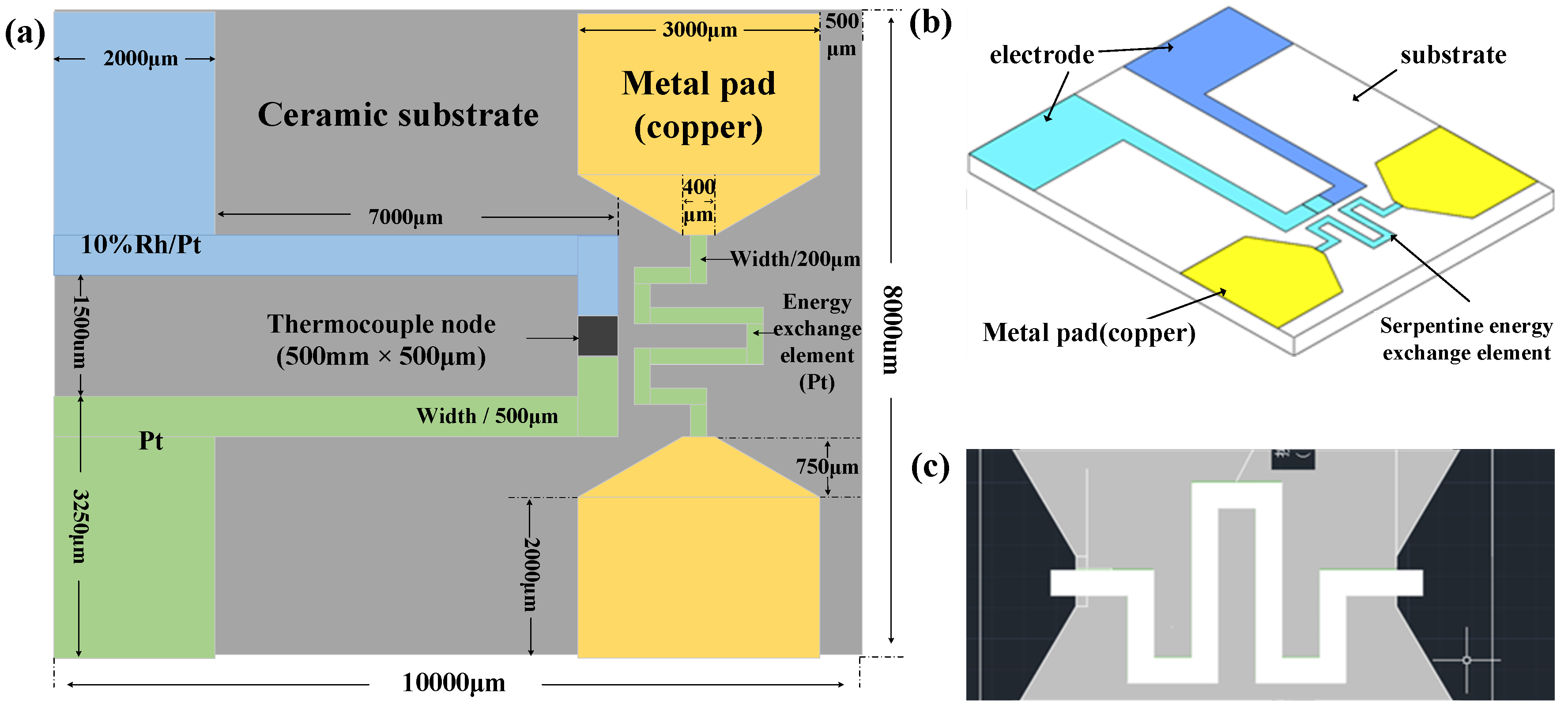
2.1. Structure
According to the general application scenarios of explosive devices, this paper selects a sheet structure to prepare a thin-film thermocouple. The structure has a smooth surface, which is conducive to better adhesion of the film layer, and can effectively fit with a variety of measured objects. The structure has high strength and good stability. The size of the micro energy commutator of the micro explosive device is generally in the millimeter level, so the size of the thin-film thermocouple developed should also be in the millimeter level. According to the working principle of a thermocouple, when two electrodes of a thermocouple contact each other, the contact potential difference will be generated in the contact area, and this contact end is the coupling junction of the sensor. At the same time, the size of the hot junction directly affects the heat capacity and response time of the thermocouple, and the response of the film thermocouple will be improved if the size of the coupling junction is controlled within 1 mm.
This article explores the various structures of thermocouples and designs the structure of the micro-sized thin-film thermocouple, as shown in
Figure 1a.
It is determined that the designed thin-film thermocouple integrated with the micro-transducer is mainly composed of a substrate and a thermoelectrode. The thermoelectrode layer is composed of thermoelectrode 1 and thermoelectrode 2 arranged in mirror symmetry along the center line of the substrate. The first electrode and the second hot electrode constitute the thermal junction of the thermocouple through the overlapping area. Among them, the micro transducer adopts a serpentine structure, which is distributed in a serpentine shape at a distance of 200 μm from the thermal junction, and is mirror-symmetrical along the center line of the ceramic substrate. The pads are symmetrically distributed on both sides, and the three-dimensional structure is shown in
Figure 1b. Among them, the thermoelectrode is 7000 μm long, 500 μm wide and 2 μm thick. The size of the even junction is 500 × 500 μm. The size of the pad is 3250 × 2000 μm, and the pad is used to connect the compensation wire.
2.2. Materials
High-purity alumina ceramics have many advantages, such as high melting point, thermal shock resistance, corrosion resistance, good wear resistance, high temperature stability and good bonding force with Pt/Rh alloy film thermoelectrode [
18]. In addition, the insulation resistance of high-purity ceramics is not less than that of ceramic materials. In view of the many advantages of ceramic materials, this paper selects high-purity alumina ceramics (99 porcelain) as the substrate for preparing thin-film thermocouples, and its structural matrix parameter is 10 mm (length) × 8 mm (width) × 0.5 mm (thickness).
According to the basic working principle of thermocouples and the law of intermediate conductors, the Seebeck coefficient of thermoelectrode material is the only factor that affects the thermoelectric potential in the closed circuit of thermocouples, and the thermoelectrode material determines the performance of thin-film thermocouples. The thermocouple made of precious metals is often used in high temperatures and harsh environments. Pt-RH10/Pt thermocouple in the thermocouple series has the advantages of high accuracy, good stability, wide temperature measurement area, long service life and high temperature measurement upper limits [
19] and is suitable for oxidation and inert atmosphere. The tungsten–rhenium thermocouple is a high melting point metal thermocouple developed gradually in order to meet the demand of temperature information measurement in high temperature environments. It is also an industrial thermocouple that can meet the demand of temperature measurement in high temperature environments above 1800 °C at present. It is widely used in aerospace, metallurgy, the nuclear industry and other high temperature industries. It has the advantages of a high melting point of alloy electrode material, high output thermoelectric potential, high sensitivity, low price, and so on.
By comparing the advantages and disadvantages of the two materials, the precious metal platinum–rhodium material is more expensive than tungsten–rhenium, and vulnerable to pollution, so the one-time investment is large; therefore, this paper has used, respectively, tungsten–rhenium materials (positive extreme W:Re = 95 wt%:5 wt%, the preparation of thin-film thermocouple with negative electrode W:Re = 74 wt%:26 wt%), platinum–rhodium alloy and pure platinum as electrode materials (positive extreme Pt-Rh10, negative extreme pure Pt) was explored [
20].
As the resistance of the transducer element increases, the critical ignition voltage of the transducer element increases in the form of a power function. When the resistance of the transducer is the same, the common Ni-Cr, Pt, and Cr materials have lower ignition voltage. Taking into account many factors such as process difficulty, fabrication cost, and material properties, the authors finally chose Pt as the transducer material for the design and integrated production of the micro-initiator [
21].
Synthesizing the process compatibility and performance requirements of thin-film thermocouples, the device structure material is determined: high-purity alumina ceramics (99 porcelain) as the matrix material and Pt metal as the energy-transducing element material. According to verification requirements and experimental conditions, W-5%Re/W-26%Re thin-film thermocouples and Pt-Rh10/Pt thin-film thermocouples were separately prepared on the substrate.
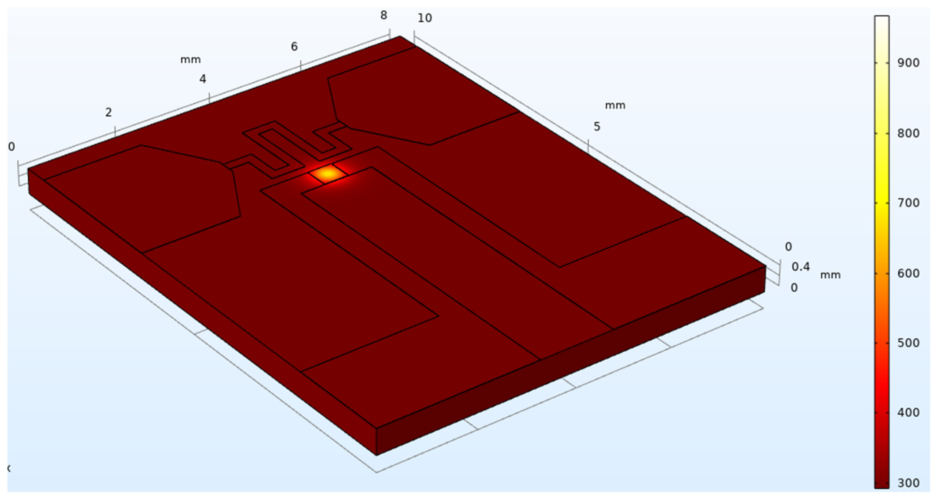
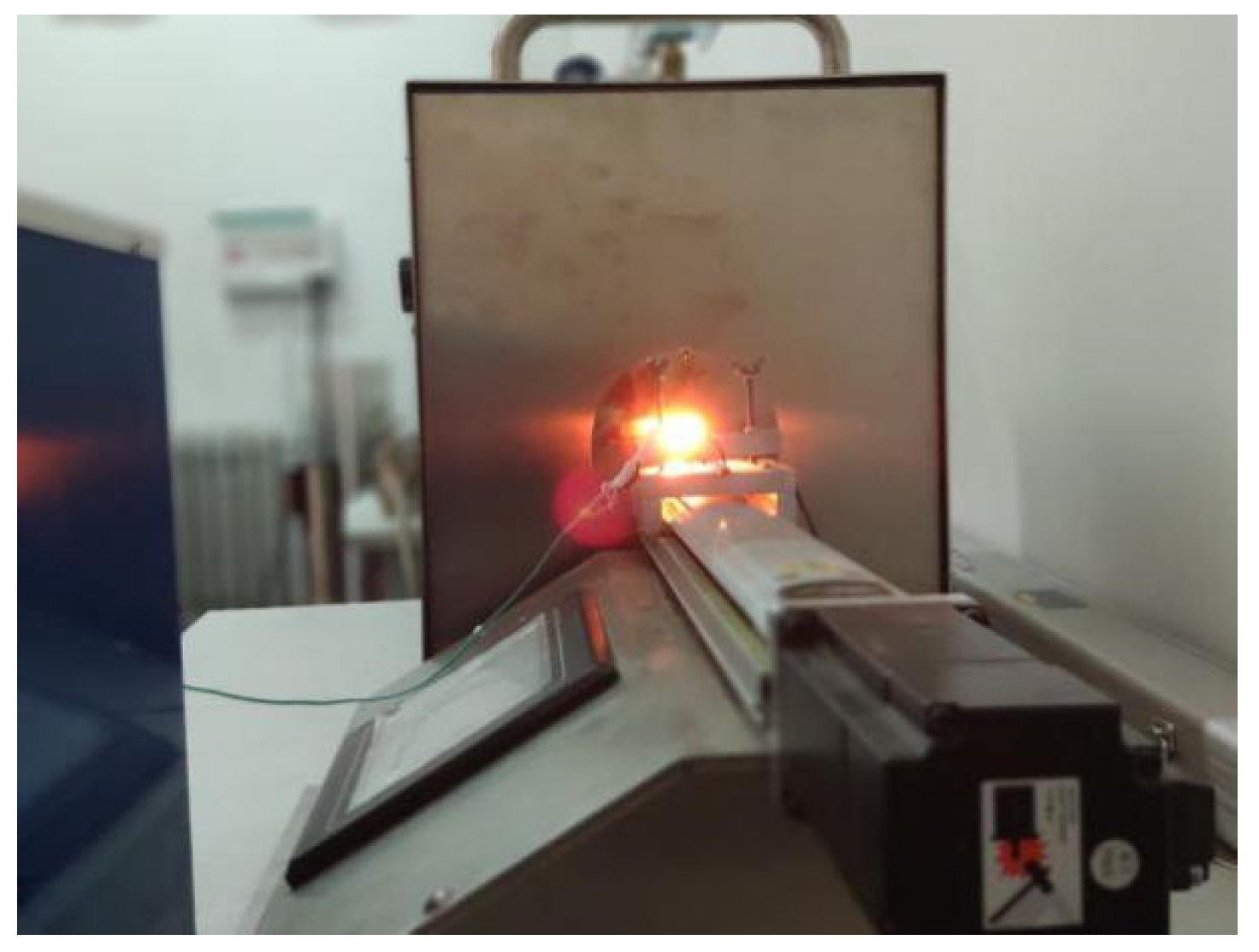
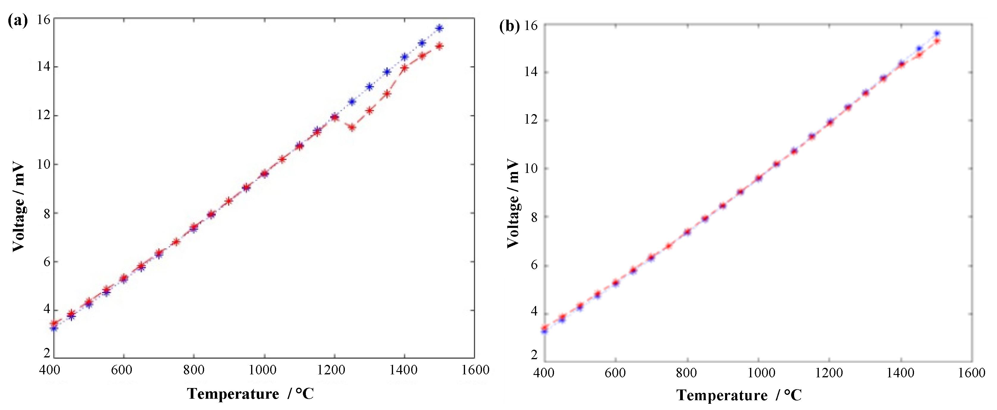
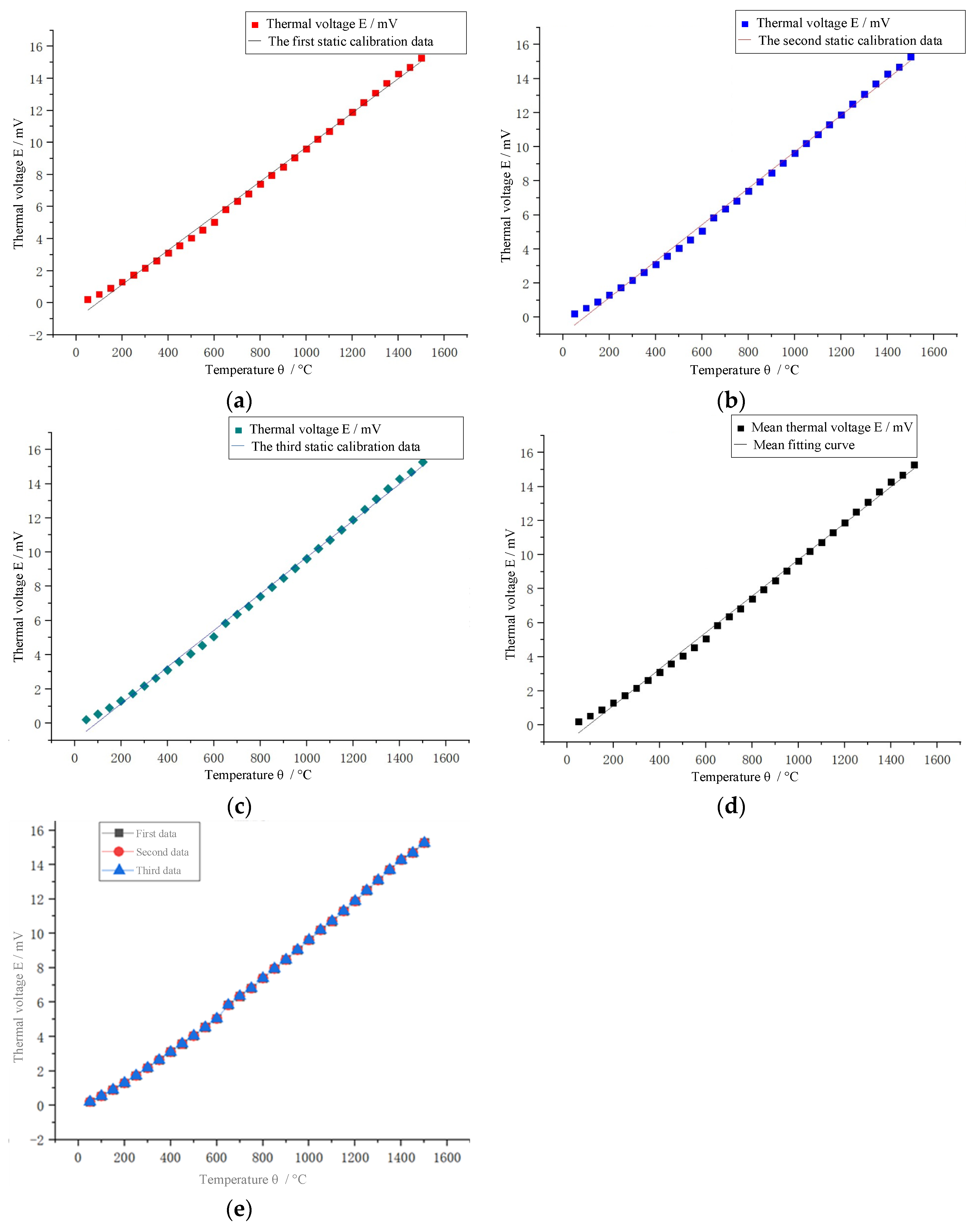
In order to understand the heat distribution of the designed structure, the Pt-Rh10/Pt thin-film thermocouple with a substrate size of 10 mm (length) × 8 mm (width) × 0.5 mm (thickness) and a junction size of (500 × 500 μm) is used as an example. Then, the corresponding element type and material properties are defined, as shown in
Figure 2. Below, the author uses Comsol finite element analysis software to simulate the designed structure and pulse laser to excite the coupling junction to simulate the heat transfer of the structure. Given that the laser spot area is smaller than the area of the thermocouple junction, it radiates heat longitudinally from the central region and has a good response. Since the properties of the material in the simulation process are selected as the thermal physical parameters of the unit solid-like material, it will inevitably lead to some errors in the thermoelectric properties of the thin film thermocouple under the simulation conditions, but the variation pattern of its temperature profile is consistent with the conventional physical properties of thermocouples.
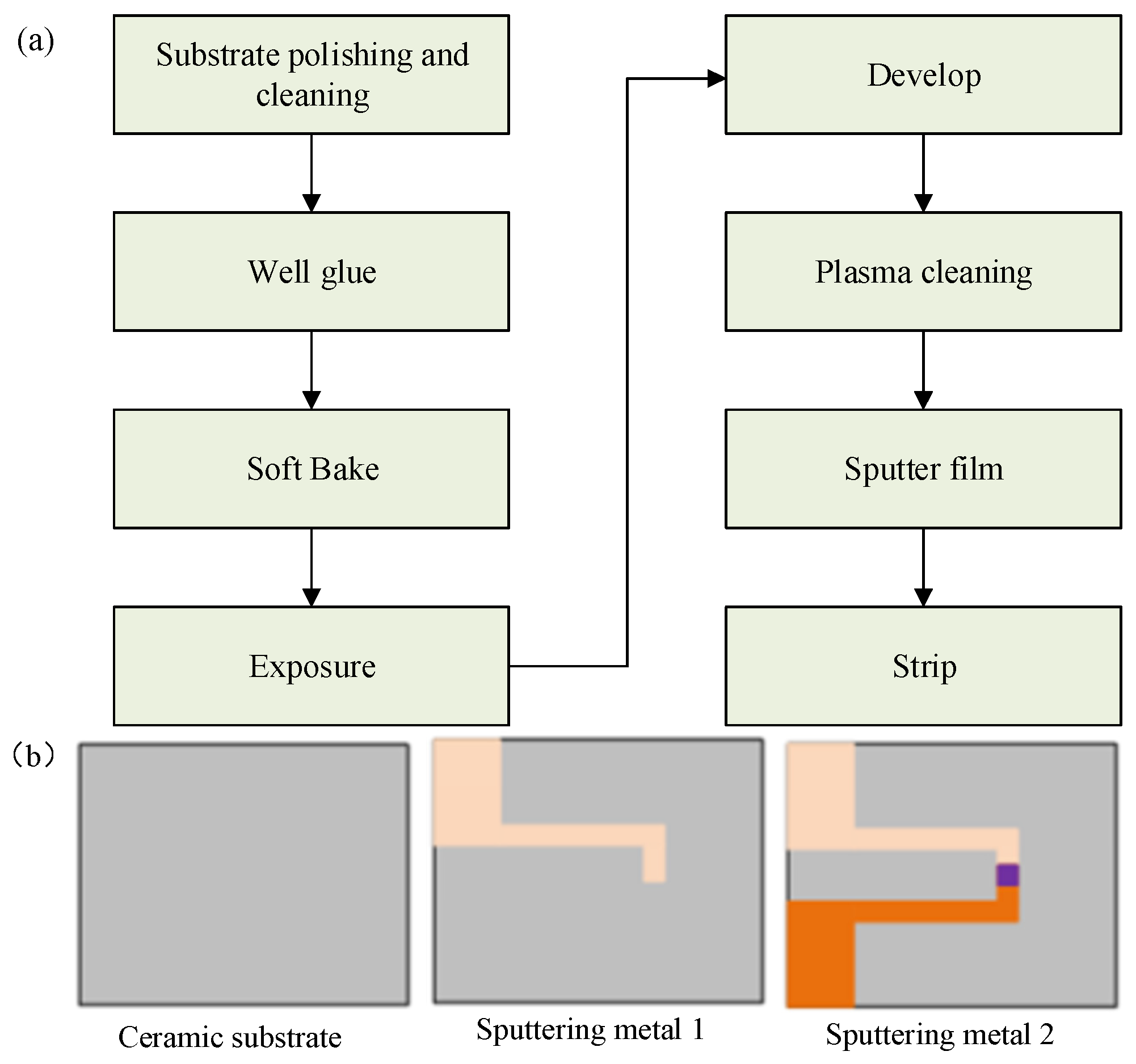
2.3. Preparation
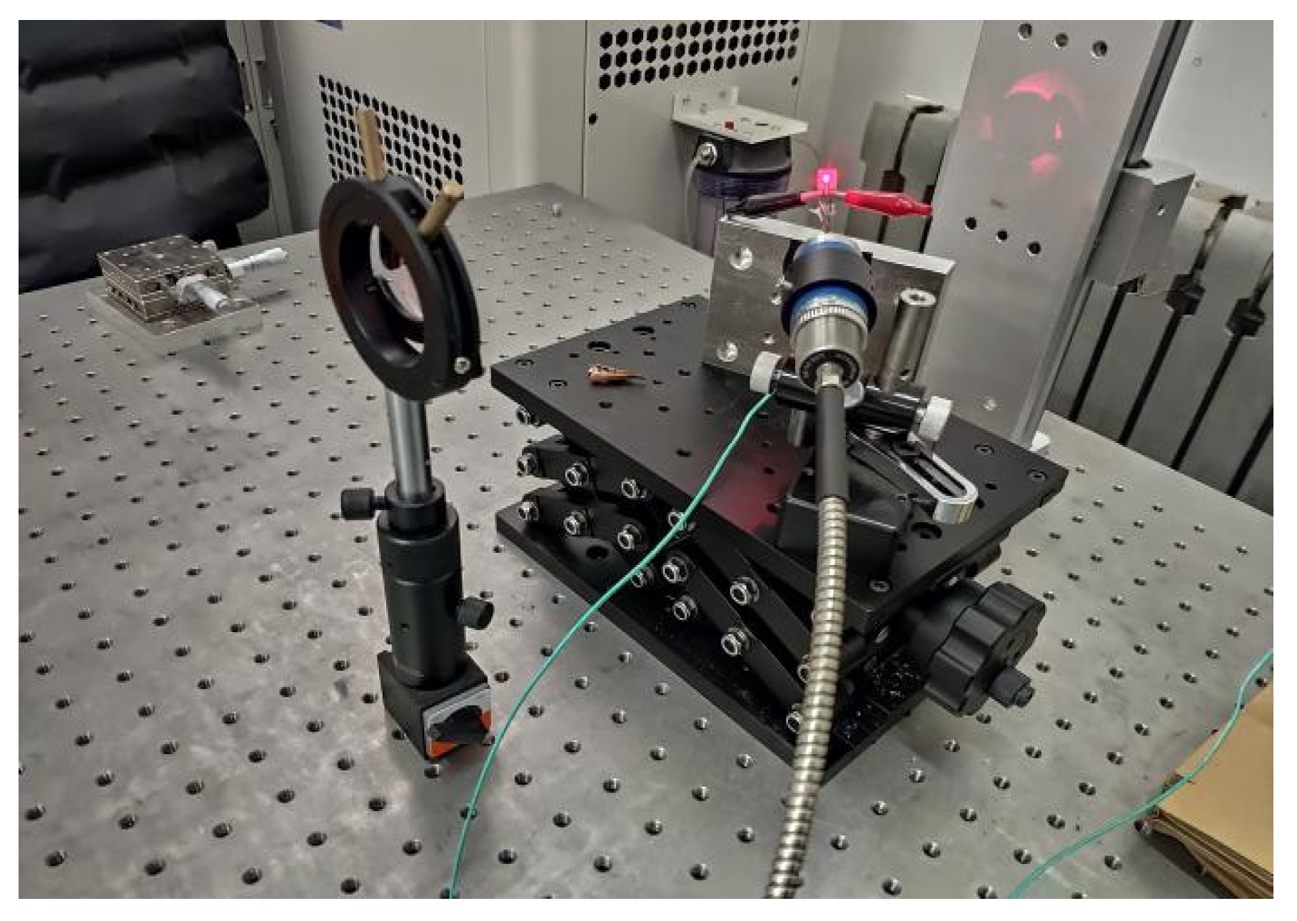
The magnetron sputtering method is adopted, and two WRe alloy targets with a purity of 99.99% with different composition ratios are used as the target materials (W:Re-95 wt%:5 wt%; W:Re-74 wt%:26 wt%; Φ76.2 mm × 6.35 mm). High-purity Ar is used as the sputtering gas, and the flow rate in working condition is 400sccm; the target base distance is adjusted to 110 mm, and then W-5%Re and W-26%Re are prepared on an Al
2O
3 ceramic substrate with a size of 10 mm × 8 mm × 0.5 mm. The detailed process and effect of thin-film thermocouple prepared by magnetron sputtering are shown in
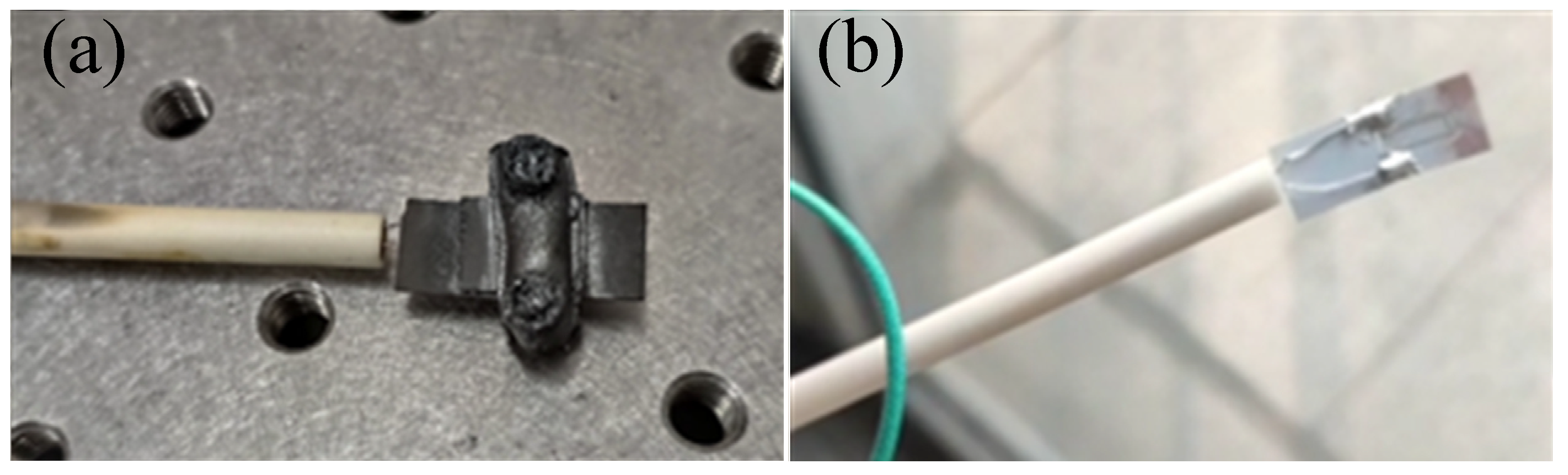
Figure 3.
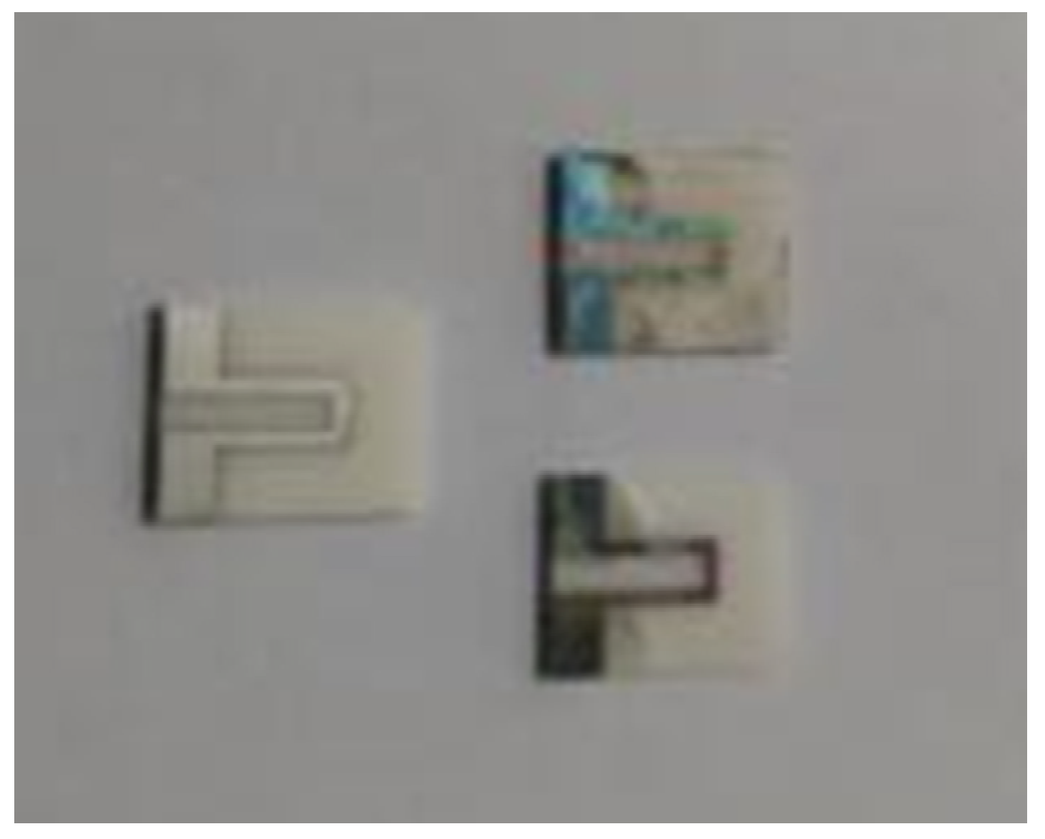
In order to not affect the electrical performance of the thin-film thermocouple, the tungsten–rhenium wire, which is the same as the electrode material, is used as the lead wire, and the tungsten paste is the welding material. When welding the lead, it was found that the bonding force between the tungsten paste and the pad was poor and easy to fall off. Then, the sample was placed in a tube furnace for high-temperature treatment; the holding temperature was 800 °C, the time was 1 h, and the heating rate was 10 °C/min. In order to prevent the tungsten–rhenium film from being rapidly oxidized, argon gas was filled in the furnace, and the flow rate of argon gas is 400 sccm. The surface morphology after heat treatment is shown in
Figure 4 below.
It can be seen that during high-temperature sintering, the organic matter of the conductive tungsten paste will volatilize during the heating process, the volume shrinks and discolors, and the shape is dry. The prepared W-5%Re/W-26%Re thin-film thermocouple still underwent oxidation in the hot end region. The film changed from silver-white metallic luster to dark green, and the film adhesion was not high. After studying the relevant literature, it is found that the tungsten–rhenium film thermocouple deposited with the Al2O3 protective layer will also fail in a short time under high-temperature environments, and the film protection process is not yet mature.
Based on previous experiments, the authors explore a low-cost and efficient preparation process, using screen printing technology to prepare Pt-Rh10/Pt thin-film thermocouples suitable for oxidizing and inert atmospheres on ceramic substrates. The preparation process is shown below.
(1) The substrate is selected and wiped with alcohol for surface hydrophilization;
(2) The platinum–rhodium conductive paste is mixed with a fineness of <15 μm with an organic carrier to make a platinum–rhodium conductive micron paste, and the platinum–rhodium electrode (left electrode) mask is placed on the insulating substrate to form a printing plate;
(3) The platinum–rhodium conductor micron paste is stacked on the printing plate and moved and pressed with a scraper to make it leak through the image area of the mask and the pores of the screen to the surface of the substrate, thereby forming a platinum–rhodium electrode film;
(4) Multi-layer printing and reinforcement of platinum and rhodium electrodes are achieved by performing leveling, drying and heat treatment on the obtained platinum rhodium electrode film and then cooled down naturally;
(5) This is replaced with a platinum electrode (right electrode) mask and a platinum electrode slurry with a fineness of <10 μm is mixed with an organic carrier to make a platinum electrode micron slurry. Step (2) to step (3) are repeated to form a platinum electrode film; the film thickness is about 6 μm;
(6) Multi-layer printing and reinforcement of the platinum electrode, film leveling, drying and heat treatment of the obtained electrode, and then natural cooling, are performed;
(7) The sample was dried in an oven and then sintered at a high temperature in a muffle furnace at 1300 °C for four hours to complete the preparation of the sensor.
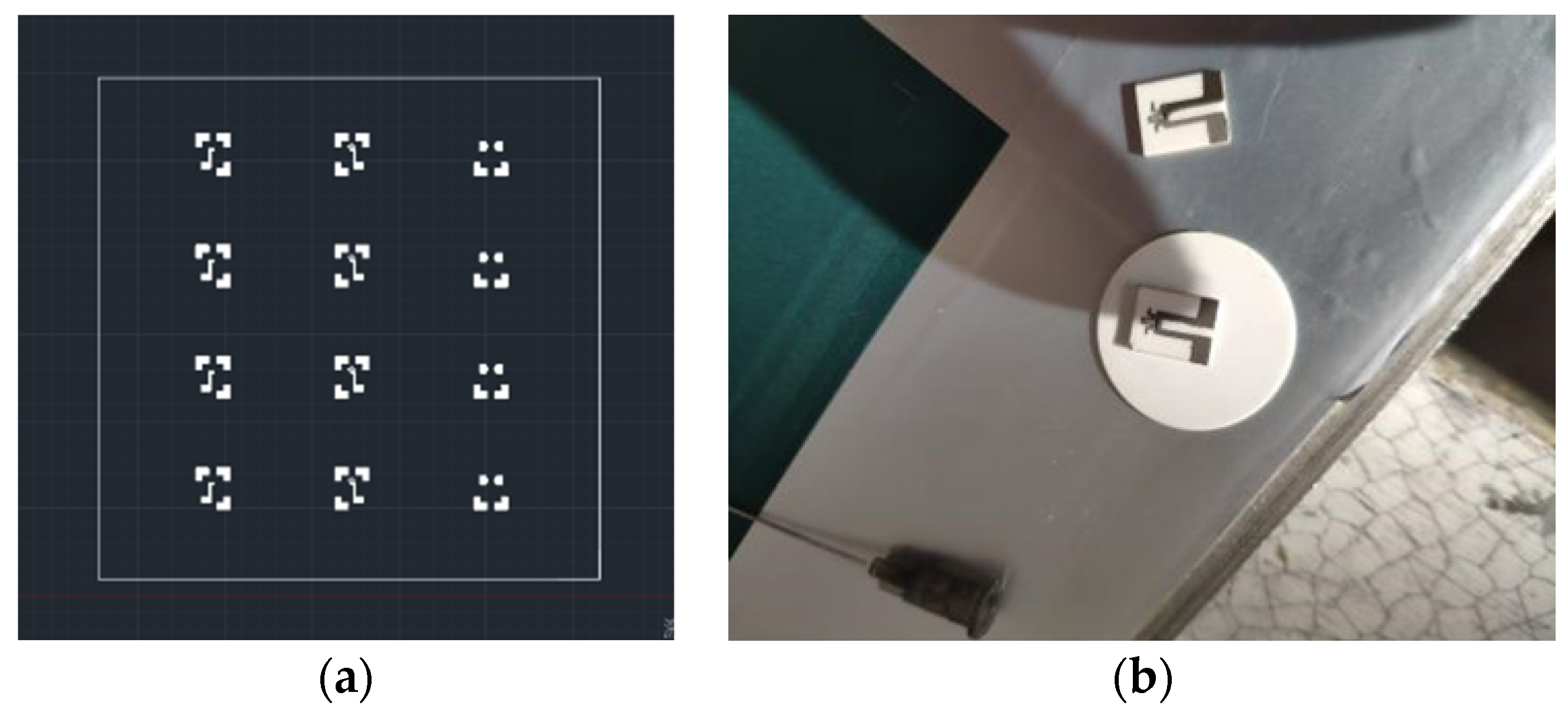
Figure 5 below shows the screen-printing stencil structure during the preparation process and the final finished film thermocouple.
In the screen-printing manufacturing process, sintering is a very important process. The film dried on the substrate must be sintered to have certain electrical properties. The sintering process is decisive for the properties and composition of the film, and its important condition is the sintering temperature. Only by sintering under the most suitable temperature and other conditions can the best properties of the materials used be obtained. After each electrode is printed, in order to make the film thickness more uniform and not easy to deform, the prepared film specimens are dried in a muffle furnace environment temperature of 200 °C for 20 min. During this period, most of the organic matter in the film will be slow. Slow volatilization enhances the adhesion of the film layer and the substrate. After the film is air-dried, the shape and performance of the dried film will not be affected when printing on the other side. At the same time, it also prevents the binder in the slurry from escaping during high-temperature sintering and causing the newly printed film to break.
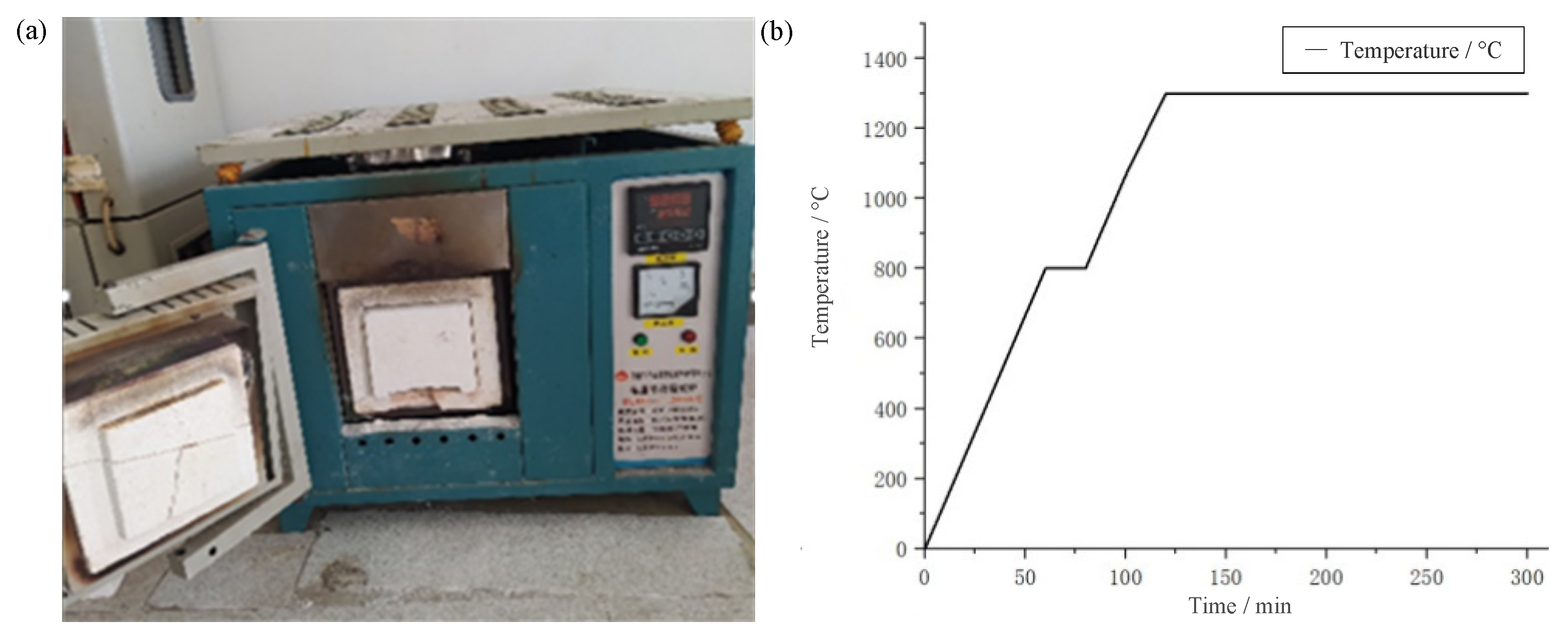
The dried thin-film thermocouple is placed in a muffle furnace for high-temperature sintering. The sintering steps include three stages of uniform heating, heat preservation and natural cooling. For different slurries, the appropriate high-temperature sintering temperature will directly affect the adhesion between the film and the substrate and the stability of the film. Too low of a temperature will result in unstable film structure and decrease in electrical conductivity. Too high of a sintering temperature will cause the crystal particle size difference in the film composition to be too large, resulting in a small oxidation reaction. Similarly, the length of the holding time will also affect the sintering effect. Too long of a holding time will continuously increase the crystal grains in the film and increase the resistance. Too short of a holding time will cause insufficient reaction of the film and lose the sintering effect. In order to improve the efficiency of preparing thin-film thermocouples and prevent excessive volatilization of organic solvents in the film, a muffle furnace with a maximum firing temperature of 1800 °C is used to fire the thin-film thermocouples during the sintering process, as shown in
Figure 6a below. The organic binder consists of resin, solvent and additives, of which the resin and solvent are ethyl cellulose and pine alcohol, respectively, and, finally, additives such as surfactants, leveling agents and defoamers are added according to actual needs. After many sintering experiments, the specific temperature rise rate when sintering the Pt-Rh10/Pt thin-film thermocouple is 7.2 °C, as shown in
Figure 6b below; the holding temperature is 1300 °C, and the holding time is 1 h. After four hours of sintering, it is cooled naturally. Intervention with cool-down can easily form internal stress in the film, which affects the stability of the film thermocouple.


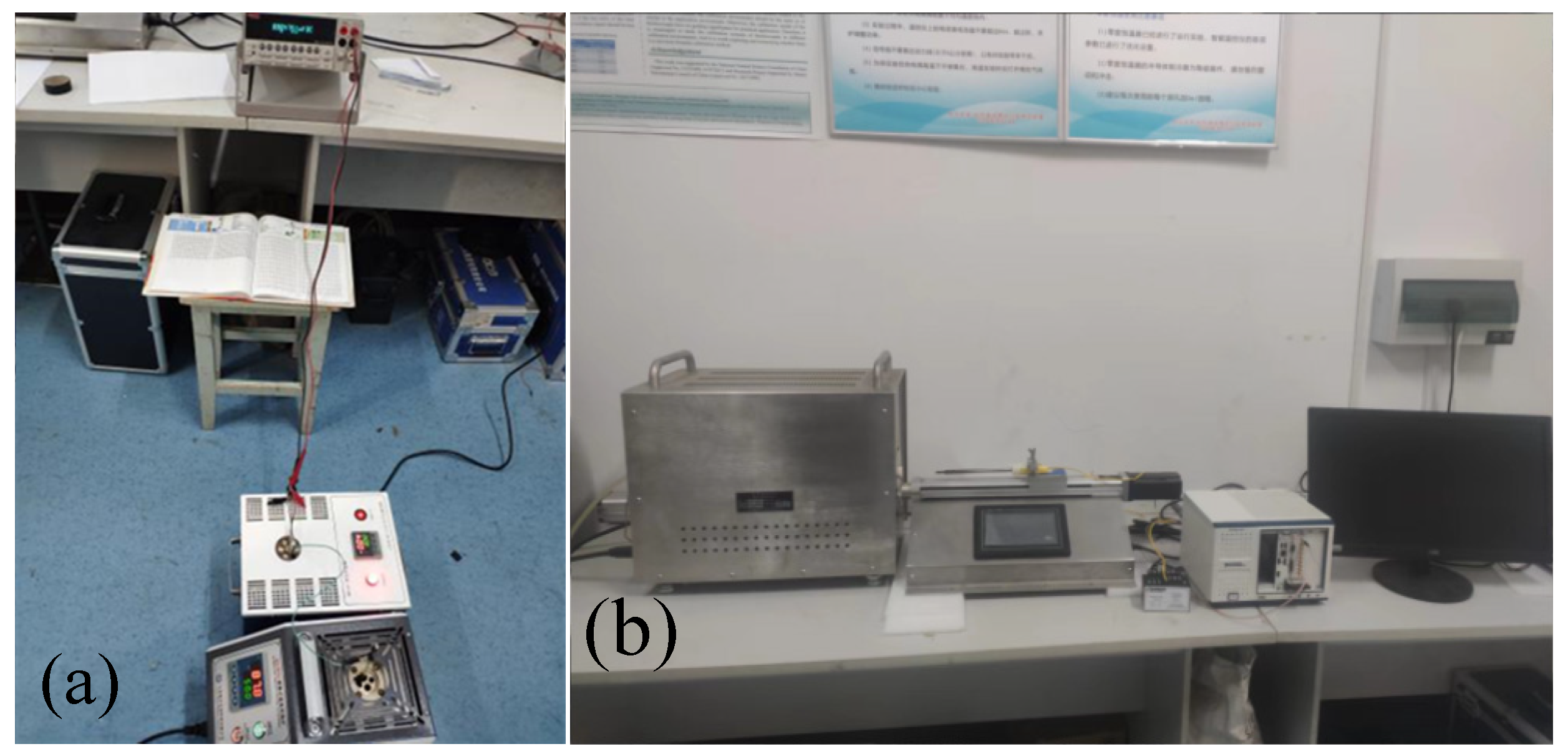
 ,
, 


