Abstract
Aggressive space mapping (ASM) is a common filter simulation and debugging method. It plays an important role in the field of microwave device design. This paper introduces ASM and presents the design and fabrication of a compact fifth-order microstrip interdigital filter with a center frequency of 2.5 GHz and a relative bandwidth of 10% using ASM. The filter used a double-layer silicon substrate structure and stepped impedance resonators (SIRs) and was optimized by ASM. After five iterations, the filter achieved the design specification, which greatly improves the efficiency of the filter design compared with the traditional method. It was fabricated on high-resistance silicon wafers by micro-electro-mechanical systems (MEMSs) technology, and the final size of the chip is 9.5 mm × 7.6 mm × 0.8 mm. The measurement results show that the characteristics of the filter are similar to the simulation results, which also shows the efficiency and precision of the ASM algorithm.
1. Introduction
Filters can select or suppress RF signals in a specific frequency range, thus combining or separating signals of different frequencies [1,2]. With the booming development of 5G communication technology [3], various microwave and millimeter wave communication systems and devices are widely used in the fields of satellite, radar, aviation, marine communication, and mobile communication [4]. Microwave filters, as an important part of them, play an irreplaceable role in frequency selection, suppressing various kinds of clutter and reducing noise interference [5,6]. Better performance, smaller size, lighter weight, and lower cost microwave filters have become the most urgent needs. Therefore, how to quickly and efficiently develop a high-performance and miniaturized filter is currently a key aspect of microwave RF filter design. The auxiliary diagnosis and debugging of filters have attracted more and more attention [7].
Space mapping [8] is an efficient means of debugging and optimizing for microwave and millimeter wave devices. It was first proposed in 1994 by Bandler and called original space mapping (OSM). It can establish a linear mapping relationship between two models (coarse model and fine model) through a large number of samples. Subsequently, an improvement in aggressive space mapping (ASM) was proposed to simplify the complex process and solve some non-linear issues [9]. Aggressive space mapping can simply establish initial mapping relations. Then, the mapping relationship between the two spaces is updated by parameter extraction. It is widely applicable to various nonlinear mapping problems [10]. Zhang et al. [11] designed a silicon-based bandpass filter with a center frequency of 24 GHz exploiting ASM. After only four iterations, the filter achieved the design specification, but the problem of high losses in the single-layer silicon substrate was also exposed. Xiao et al. [12] designed a double-layer silicon-based stripline filter with a center frequency of 20.76 GHz. After five iterations, the filter meets the design requirements. This filter had a lower loss, but its size is too big for a microwave system. In addition, many researchers used ASM in the debugging of filters and verified the feasibility and effectiveness of ASM in filter design [13,14,15,16,17].
To overcome the problems of large size and high loss of silicon-based filters, this paper proposes a filter structure with a double-layer silicon substrate and stepped impedance resonators (SIRs) [18,19,20]. As shown in Figure 1, this structure is similar to substrate integrated waveguide (SIW) [21], the double-layer high resistance silicon substrate, and surrounding TSV metalized vias enclosing the transmission line. The coplanar waveguide with a characteristic impedance of 50 Ω was used for the input and output interface of the filter. The structure not only reduces electromagnetic leakage and improves filter performance, it also reduces the filter volume.
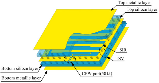
Figure 1.
The structure of the double-layer silicon-based interdigital filter.
2. Theory and Design
2.1. General Formulation of ASM
Aggressive space mapping is an efficient optimization algorithm that is widely used in the design of microwave devices and microwave circuits. It establishes a dynamic mapping relationship between the coarse model and fine model so that the complex and time-consuming optimization problem of the fine model is transformed into simple and fast optimization and updating of the coarse model. While realizing fast and efficient optimization, some nonlinear problems can be resolved.
In the process of solving by the ASM algorithm, represents the optimal design parameter of the coarse model and represents the coarse model response. The coarse model and fine model meet the following requirements in a small range:
The next design parameters of the fine model are updated by the quasi-Newton iteration, as follows:
where is given by
If the iteration step length is a quasi-Newtonian step length, the solution of can be updated using the Broyden formula, which satisfies the quasi-Newton update formula:
When the space physical meaning of the coarse model and fine model is the same,
where I is the identity matrix and the super-index T stands for transpose.
2.2. Basic Principles of SIR
Uniform impedance resonators (UIRs) [22] and step impedance resonators (SIRs) are common transmission line type resonators, widely used in microwave filters design. Step impedance resonators (SIRs) are simple in structure, easy to design, and able to reduce the length of the resonator without changing the unloaded Q value. Compared with UIR, SIR has more advantages in terms of structural form, harmonic suppression, design parameter control, and filter miniaturization.
Stepped impedance resonators (SIRs) are a kind of resonator composed of more than two transmission lines with different characteristic impedance and capable of transmitting TEM mode or quasi-TEM mode. It comes in three types: , , and , where the -type resonators, owing to a small volume and the fact that the parasitic frequency band is three times the center frequency, have been widely used in small volume filters’ design. As shown in Figure 2, the characteristic impedance and equivalent electrical length of the open-circuit end and short-circuit end are (Z1,θ1) and (Z2,θ2), respectively.
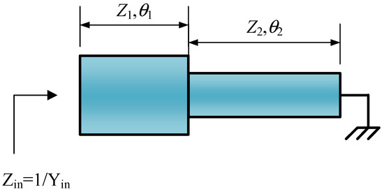
Figure 2.
The basic structure of a λg/4-type SIR.
According to Figure 2, its input impedance can be expressed as follows:
Defining the impedance ratio , when Yin = 1/Zin = 0, as in Equation (7), the -type SIR achieves the resonance condition.
Therefore, the -type resonance conditions are related to , , and . Compared with ordinary microstrip line resonators, -type SIR has one more design degree of freedom, which has greatly promoted the specific application of various SIR resonators.
In general, compared with conventional uniform impedance resonators (UIR) whose electric length is , the normalized resonator length of -type resonators is as follows:
Figure 3 is the curve graph between the normalized resonator length and the electric length when the impedance ratio RZ is different. According to Figure 3, in the process of designing filters using SIR, a smaller impedance ratio should be chosen so that the filter size can be reduced and the original transmission performance of the resonator can be maintained as much as possible. In the design process, the commonly used impedance ratio = 0.8 [23].
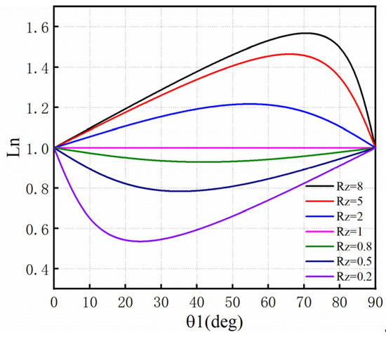
Figure 3.
Resonance conditions of SIR.
2.3. Design and Optimization
In this paper, a fifth-order microstrip interdigital filter was designed with a center frequency of 2.5 GHz, a bandwidth of 0.25 GHz, and a passband Ripple of 0.1 dB. The 2D structure of this filter is shown in Figure 4.
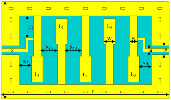
Figure 4.
Two-dimensional structure of the fifth-order interdigital filter.
The ASM algorithm involves coarse and fine models that are based on physical parameters. Then, a mapping relation is established between the two models using a mapping matrix for quick design and optimization. The fine and coarse models of this filter are represented by the HFSS model and its normalized coupling matrix M. According to the design index of the filter, the normalized coupling matrix M of the filter is obtained by the Chebyshev synthesis method [24]:
Based on the normalized coupling matrix M, the coupling coefficient Kij and the external quality factor Qe of the filter can be derived. c is a vector representing the ideal center frequency, coupling coefficient, and external quality factor:
c = [f1 = 2.5 GHz, f2 = 2.5 GHz, f3 = 2.5 GHz, m12 = 0.797, m23 = 0.607, Qe = 11.48]
Therefore, six physical quantities need to be optimized, and the parameter optimization vector of the coarse model is as follows:
xc = [L1, L2, L3, S1,2, S2,3, Lt]T
Then, the resonant frequency f0 and external quality factor Qe of the single resonator and the coupling coefficient K between two resonators of this filter are extracted by the 3D electromagnetic simulation software Ansoft HFFSS’s eigenmode solution model. The extraction of coupling coefficients K requires the creation of two single-cavity resonators placed side-by-side. At this point, the inherent resonant frequency f0 of the resonator is decomposed into two new frequencies f1 and f2 owing to the coupling effect. The coupling coefficient K can be solved by f1 and f2 as in Equation (9):
The simulation relationship between these physical quantities (f0, Qe, and K) and optimization variables is established, as shown in Figure 5.
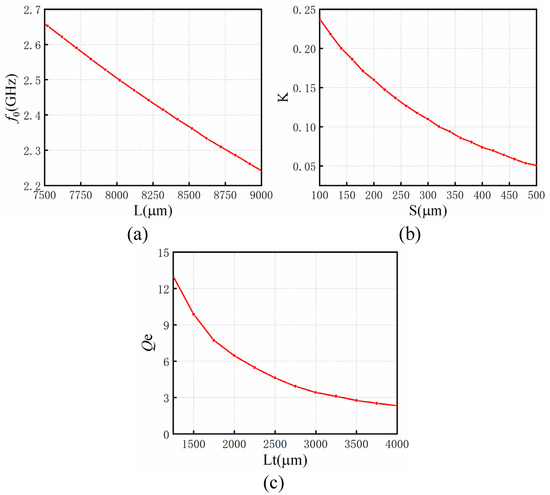
Figure 5.
(a) Relationship between center frequency f0 and resonator length L. (b) Relationship between coupling coefficient K and distance S. (c) Relationship between external quality factor Qe and tapped position Lt.
According to Figure 5, the initial physical size of the filter x = [385, 457, 1380, 8046, 8046, 8046]T, and its unit is um. Then it was modeled and simulated by Ansoft HFFSS by Ansoft Corporation, Pittsburgh, PA, USA. Its initial response is shown in Figure 6a. This did not meet the index requirements. The optimization process of applying ASM to the bandpass filter is described as follows:
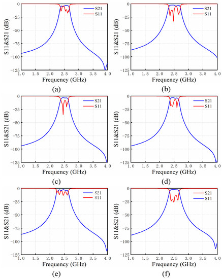
Figure 6.
(a) Initial response of the filter. (b) Response after the first iteration. (c) Response after the second iteration. (d) Response after the fourth iteration. (e) Response after the fifth iteration. (f) Response after the sixth iteration.
- (1)
- Initialize , , extract the S parameter of the initial response by the Cauchy method and calculate the corresponding coupling matrix. Calculate through Figure 5, and obtain the current mapping error ;
- (2)
- Calculate fine model design parameter growth step using Equation (3), and work out the design parameters for the next step of the fine model ;
- (3)
- Perform the fine mode simulation in HFSS and obtain the responses in Figure 6b, which still does not meet the design index and needs to be further optimized;
- (4)
- Perform parameter extraction, extract the design parameters of the rough model , and calculate the mapping error ;
- (5)
- Update the mapping relation matrix to through Equation (4);
- (6)
- , return to step 3 and continue executing the program until the response of the filter satisfies the design metrics.
As shown in Figure 6f, after the fifth iteration, the filter satisfies the design specifications.
The optimized parameters of the filter after each iteration are shown in Table 1.

Table 1.
The optimization parameter in each iteration (unit: µm).
3. Fabrication and Measurement
The above-mentioned interdigital filter can be fabricated by MEMS processing technology, which mainly includes bulk silicon, microsurface, and metallic bonding technology. Its substrate is a kind of high-resistivity silicon (>10 KΩ·cm) with a thickness of 400 µm. The main process steps involved are photolithography, ICP etching, coating, electroplating, corrosion, and bonding. The fabrication process is shown in Figure 7.
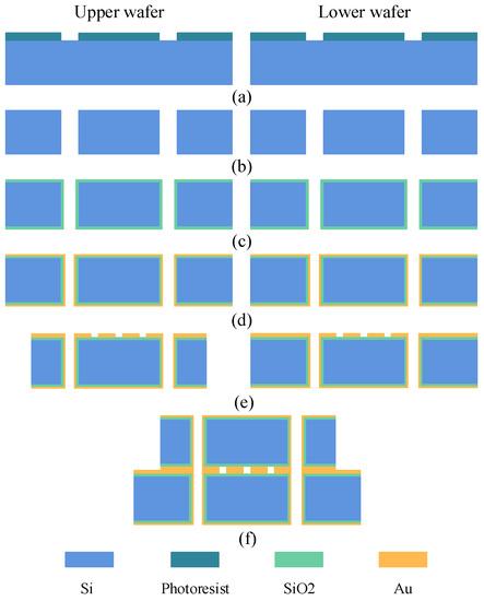
Figure 7.
The fabrication processes of the interdigital filter. (a) Pattern the hole photoresist. (b) Etching via-hole. (c) Preparation of isolation layer. (d) Sputter the seed layer. (e) Electroplating surface structure. (f) Au–Au bonding.
Firstly, a 10-micron thick photoresist was spin-coated on the silicon wafer surface and the pattern of the holes was transferred to the photoresist by photolithography. Secondly, holes were etched on the silicon wafer by the inductively coupled plasma (ICP) etching process. Thirdly, a 0.5-micron thick SiO2 isolation layer was then grown on the surface of the wafer and the sidewalls of the TSV by a high-temperature thermal oxygen process. Fourthly sputtered adhesion and seed layers of 50 nm Ti and 250 nm Au, respectively, on the wafer surface; then electroplate resonator and ground plane on wafer surface using photoresist as plating die and removing the seed layer and adhesion layer by wet etching. Finally, Au–Au thermal-compression bonding. The final size of the chip is 9.5 mm × 7.6 mm × 0.8 mm. The photograph of the fabricated filter is shown in Figure 8.
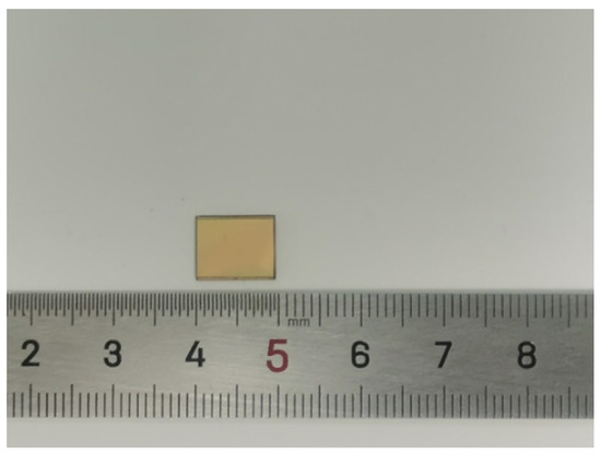
Figure 8.
Photograph of the fabricated filter.
The filter was tested with a PNA-N5227B vector network analyzer manufactured by KEYSIGHT (Santa Rosa, CA, USA) with a measurement range of 10 MHz to 67 GHz. Furthermore, a pair of TITAN-RC-200 probes and a YB600 probe station were used. A comparison of the simulation and measurement results is shown in Figure 9. It can be seen that the simulation curve and the actual measured curve do not coincide completely, but they are similar. The simulation results show that the insertion loss of this filter at 2.5 GHz is 2.1 dB, the out-of-band rejection is 40 dB, and the return loss is 15 dB; the measured results show that the insertion loss of this filter at 2.5 GHz is 3.2 dB, the out-of-band rejection is 21 dB, and the return loss is 17 dB. By considering the errors in processing and measurement, the measured performance of the filter is reduced, but within a certain range, the method of designing and optimizing the filter using ASM can be adopted.
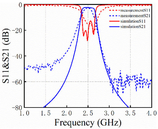
Figure 9.
Simulation and measurement results of the proposed filter.
4. Conclusions
This paper mainly introduces the application prospect of the bandpass filter and the important role of ASM in microwave device design. Then, a compacted S-band interdigital bandpass filter with stepped impedance resonators (SIRs) was designed with ASM after five iterations. It was fabricated on high-resistance silicon wafers by the MEMS process, which is conducive to the miniaturization and integration of communication systems. The test results and design results of the filter remain highly consistent, despite some differences caused by process errors. In summary, aggressive space mapping is a fast and efficient method to optimize the design of microwave devices.
Author Contributions
Q.W.: conceptualization, methodology, writing—original draft preparation, and project administration; X.G.: software and data curation; Z.S.: validation; J.L.: visualization; M.L.: supervision and funding acquisition. All authors have read and agreed to the published version of the manuscript.
Funding
This research was funded by Equipment Development Department New Product Project, Shanxi Province Postgraduate Education Reform Project, “Double First-Class” disciplines National first-class curriculum construction, and National Future Technical College Construction Project, grant number 2006WW0011, 110121, 11013168, and 11013169.
Acknowledgments
We thank Suzhou Institute of Nano-Tech and Nano-Bionics (SINANO), Chinese Academy of Science for their processing technology support.
Conflicts of Interest
The authors declare no conflict of interest. The funders had no role in the design of the study; in the collection, analyses, or interpretation of data; in the writing of the manuscript; or in the decision to publish the results.
References
- Syms, R.; Bouchaala, A. Mechanical synchronization of MEMS electrostatically driven coupled beam filters. Micromachines 2021, 12, 1191. [Google Scholar] [CrossRef] [PubMed]
- Han, L.; Wang, Y.; Wu, Q.; Zhang, S.; Wang, S.; Li, M. A novel low-loss four-bit bandpass filter using RF MEMS switches. Chin. Phys. B 2021, 31, 018506. [Google Scholar] [CrossRef]
- Liu, Y.; Cai, Y.; Zhang, Y.; Tovstopyat, A.; Liu, S.; Sun, C. Materials, design, and characteristics of bulk acoustic wave resonator: A review. Micromachines 2020, 11, 630. [Google Scholar] [CrossRef] [PubMed]
- Luo, T.; Liu, Y.; Zou, Y.; Zhou, J.; Liu, W.; Wu, G.; Cai, Y.; Sun, C. Design and Optimization of the Dual-Mode Lamb Wave Resonator and Dual-Passband Filter. Micromachines 2022, 13, 87. [Google Scholar] [CrossRef] [PubMed]
- Zhang, W.; Feng, F.; Liu, W.; Yan, S.; Zhang, J.; Jin, J.; Zhang, Q. Advanced parallel space-mapping-based multiphysics optimization for high-power microwave filters. IEEE Trans. Microw. Theory Tech. 2021, 69, 2470–2484. [Google Scholar] [CrossRef]
- Deng, Z.; Wei, H.; Guo, X. 21.69–24.36 GHz MEMS tunable band-pass filter. Micromachines 2016, 7, 149. [Google Scholar] [CrossRef]
- Zhang, X.; Ou, W.; Ou, Y. Design and optimization of a planar folded substrate integrated waveguide bandpass filter exploiting aggressive space mapping. Int. J. RF Microw. Comput.-Aided Eng. 2019, 29, e21713. [Google Scholar] [CrossRef]
- Bandler, J.W.; Biernacki, R.M.; Chen, S.H.; Grobelny, P.A.; Hemmers, R.H. Space mapping technique for electromagnetic optimization. IEEE Trans. Microw. Theory Tech. 1994, 42, 2536–2544. [Google Scholar] [CrossRef]
- Bandler, J.W.; Biernacki, R.M.; Chen, S.H.; Hemmers, R.H.; Madsen, K. Electromagnetic optimization exploiting aggressive space mapping. IEEE Trans. Microw. Theory Tech. 1995, 43, 2874–2882. [Google Scholar] [CrossRef]
- Rayas-Sanchez, J.E. Power in simplicity with ASM: Tracing the aggressive space mapping algorithm over two decades of development and engineering applications. IEEE Microw. Mag. 2016, 17, 64–76. [Google Scholar] [CrossRef]
- Zhang, X.; Ou, Y.; Ou, W. Design of a silicon-based wideband bandpass filter using aggressive space mapping. IEICE Electron. Express 2018, 15, 20180897. [Google Scholar] [CrossRef]
- Xiao, S.; Huai, Y.; Ou, W.; Liu, J.; Ou, Y. Investigation on temperature stability of MEMS silicon-based sixth-order stripline filter. Int. J. RF Microw. Comput.-Aided Eng. 2021, 31, e22836. [Google Scholar] [CrossRef]
- Melgarejo, J.C.; Ossorio, J.; Cogollos, S.; Guglielmi, M.; Boria, V.E.; Bandler, J.W. On space mapping techniques for microwave filter tuning. IEEE Trans. Microw. Theory Tech. 2019, 67, 4860–4870. [Google Scholar] [CrossRef]
- Sans, M.; Selga, J.; Rodríguez, A.; Bonache, J.; Boria, V.E.; Martín, F. Design of planar wideband bandpass filters from specifications using a two-step aggressive space mapping (ASM) optimization algorithm. IEEE Trans. Microw. Theory Tech. 2014, 62, 3341–3350. [Google Scholar] [CrossRef]
- Rodríguez, A.; Selga, J.; Sans, M.; Martín, F.; Boria, V. Automated design of bandpass filters based on open complementary split ring resonators (OCSRRs) using aggressive space mapping (ASM) optimization. Int. J. Numer. Model. Electron. Netw. Devices Fields 2017, 30, e2121. [Google Scholar] [CrossRef]
- Ossorio, J.; Melgarejo, J.C.; Boria, V.E.; Guglielmi, M.; Bandler, J.W. On the alignment of low-fidelity and high-fidelity simulation spaces for the design of microwave waveguide filters. IEEE Trans. Microw. Theory Tech. 2018, 66, 5183–5196. [Google Scholar] [CrossRef]
- Sans, M.; Selga, J.; Vélez, P.; Rodríguez, A.; Bonache, J.; Boria, V.E.; Martín, F. Automated design of balanced wideband bandpass filters based on mirrored stepped impedance resonators (SIRs) and interdigital capacitors. Int. J. Microw. Wirel. Technol. 2016, 8, 731–740. [Google Scholar] [CrossRef]
- Weng, M.H.; Tsai, C.Y.; Chen, D.L.; Chung, Y.C.; Yang, R.Y. A bandpass filter using half mode SIW structure with step impedance resonator. Electronics 2020, 10, 51. [Google Scholar] [CrossRef]
- Benedicto, J.; Aouidad, M.H.; Rius, E.; Favennec, J.F.; Martin-Guennou, A.; Manchec, A. Analytical Modeling of Three-Section Coaxial Stepped Impedance Resonators for the Design of Compact Tx Bandpass Filters. IEEE Trans. Microw. Theory Tech. 2022, 70, 4140–4155. [Google Scholar] [CrossRef]
- Liu, L.; Zhang, P.; Weng, M.H.; Tsai, C.Y.; Yang, R.Y. A miniaturized wideband bandpass filter using quarter-wavelength stepped-impedance resonators. Electronics 2019, 8, 1540. [Google Scholar] [CrossRef]
- Ho, M.H.; Tang, K.H. Miniaturized SIW cavity tri-band filter design. IEEE Microw. Wirel. Compon. Lett. 2020, 30, 589–592. [Google Scholar] [CrossRef]
- Liu, L.Q.; Yang, Q.Q.; Chen, D.L.; Weng, M.H.; Yang, R.Y. Design of tri-band bandpass filter using uniform impedance resonators loaded with different impedance stubs. Electromagnetics 2021, 41, 253–262. [Google Scholar] [CrossRef]
- Sagawa, M.; Makimoto, M.; Yamashita, S. Geometrical structures and fundamental characteristics of microwave stepped-impedance resonators IEEE Trans. Microw. Theory Tech. 1997, 7, 1078–1085. [Google Scholar] [CrossRef]
- Mishra, V.; Singh, A.K. Design and analysis of coupling matrix for microwave filter applications VSRD Int. J. Electr. Electron. Commun. Eng. 2012, 7, 508–520. [Google Scholar]


Disclaimer/Publisher’s Note: The statements, opinions and data contained in all publications are solely those of the individual author(s) and contributor(s) and not of MDPI and/or the editor(s). MDPI and/or the editor(s) disclaim responsibility for any injury to people or property resulting from any ideas, methods, instructions or products referred to in the content. |
© 2022 by the authors. Licensee MDPI, Basel, Switzerland. This article is an open access article distributed under the terms and conditions of the Creative Commons Attribution (CC BY) license (https://creativecommons.org/licenses/by/4.0/).