Article

Investigation of the Electrical Coupling Effect for Monolithic 3-Dimensional Nonvolatile Memory Consisting of a Feedback Field-Effect Transistor Using TCAD

ICT & Robotics Engineering, Semiconductor Convergence Engineering, AISPC Laboratory and IITC, Hankyong National University, 327 Jungang-ro, Anseong-si 17579, Gyenggi-do, Republic of Korea
*
Author to whom correspondence should be addressed.
Micromachines 2023, 14(10), 1822; https://doi.org/10.3390/mi14101822
Submission received: 15 August 2023 / Revised: 11 September 2023 / Accepted: 20 September 2023 / Published: 23 September 2023
(This article belongs to the Special Issue Recent Advances in Memory Materials and Devices)

Abstract

:
In this study, the electrical characteristics and electrical coupling effect for monolithic 3-dimensional nonvolatile memory consisting of a feedback field-effect transistor (M3D-NVM-FBFET) were investigated using technology computer-aided design. The M3D-NVM-FBFET consists of an N-type FBFET with an oxide–nitride–oxide layer and a metal–oxide–semiconductor FET (MOSFET) in the top and bottom tiers, respectively. For the memory simulation, the programming and erasing voltages were applied at 18 and −18 V for 1 μs, respectively. The memory window of the M3D-NVM-FBFET was 1.98 V. As the retention simulation was conducted for 10 years, the memory window decreased from 1.98 to 0.83 V. For the M3D-NVM-FBFET, the electrical coupling that occurs through an electrical signal in the bottom-tier transistor was investigated. As the thickness of the interlayer dielectric (TILD) decreases from 100 to 10 nm, the change in the VTH increases from 0.16 to 0.87 V and from 0.15 to 0.84 V after the programming and erasing operations, respectively. M3D-NVM-FBFET circuits with a thin TILD of 50 nm or less need to be designed considering electrical coupling.

1. Introduction

In recent decades, the scaling of transistors has continuously been improved, and the fabrication technology node of a metal–oxide–semiconductor field-effect transistor (MOSFET) has reached the nanoscale. However, the technical challenges of nanoscale transistors make it difficult to increase transistor integration [1]. Moreover, the 2-dimensional planar structure of the MOSFET has secondary effects such as a short-channel effect [2]. To overcome these limitations, various solutions have been suggested in terms of devices and circuit design [3,4,5,6,7,8,9,10]. Among them, monolithic 3-dimensional integration (M3DI), which allows the vertical stacking of transistors, logic gates, and memory devices, is a promising technology for future chip design [11,12,13,14,15]. Consequently, M3D structures have been researched in terms of transistors, logic gates, and system-level applications. For M3D structures, the transistor density within the same area is higher than that of conventional 2D structures. Moreover, the critical delay of M3DI is low due to vertical interconnection, which is shorter than horizontal interconnection [16]. In most of the configuration of the M3D structure, the logic gates are located in the lowest layer and the memory circuits and systems are designed in the upper layer [17,18,19]. To facilitate the stacking of each system, an investigation of the memory device, circuit, and system with a stackable structure is required.
One of the candidates for a next-generation memory device is a feedback field-effect transistor (FBFET). The FBFET exhibits an approximately zero slope and hysteresis characteristics [20,21,22]. Various circuits consisting of FBFETs operating as logic [23,24,25], memory circuits [26,27,28], and neuromorphic circuits [29,30] have been presented. In particular, the basic fabrication of the FBFET is based on the complementary metal–oxide–semiconductor (CMOS) technology; therefore, memory circuits configured with the FBFET have received attention as a next-generation memory system considering fabrication costs. Recently, a nonvolatile memory FBFET (NVM-FBFET) with a nanowire structure was suggested [31]. This NVM-FBFET demonstrates fast erasing and programming times (~1 μs) compared with conventional flash memory. Moreover, the suggested NVM-FBFET can operate as volatile memory (VM) using hysteresis characteristics. When using NVM-FBFET as volatile memory, the hysteresis characteristics themselves do not require a capacitor. This characteristic offers advantages for increasing the memory capacity through transistor scaling, whereas the conventional dynamic random access memory is challenged to increase density due to capacitor scaling [32]. When the VM-FBFET is designed with a M3D structure, data transmission is faster due to the reduced physical distance between NVM and VM. Additionally, the data bus width can be increased by stacking the memory circuits, as has already been realized by high-bandwidth memory [33]. However, the structure of the suggested NVM-FBFET makes it difficult to stack vertically. The nanowire structure can be designed as a 3D structure at the transistor level, but designing a 3D structure with circuits or at the system level is challenging. In order to stack the NVM-FBFET vertically for M3D design, an investigation of the stackable structure of the NVM-FBFET is required.
When designing the M3D structure, the electrical coupling between the top and bottom transistors or the monolithic interlayer via (MIV) occurs [34]. The electrical characteristics of the top-layer transistor were changed due to electrical coupling by the bottom-layer transistors or MIVs. The electrical coupling effects of the various circuits configured with MOSFETs [35], junction-less FETs [36,37], and FBFETs [38,39] have already been investigated. In the case of the NVM-FBFET, the investigation of the electrical coupling has not been conducted yet. For the M3D-NVM-FBFET, the current level considering the electrical coupling is an important factor that decides the ‘0’ and ‘1’ of a bit. Hence, the electrical coupling must be investigated before designing the M3D-NVM-FBFET.
In this paper, the electrical characteristics and the electrical coupling of the M3D-NVM-FBFET are investigated using technology computer-aided design (TCAD). First, the simulation structure of the M3D-NVM-FBFET will be explained in Section 2. Then, the electrical characteristics and the electrical coupling of the M3D-NVM-FBFET will be discussed in Section 3. Finally, the conclusions of this study will be described in Section 4.

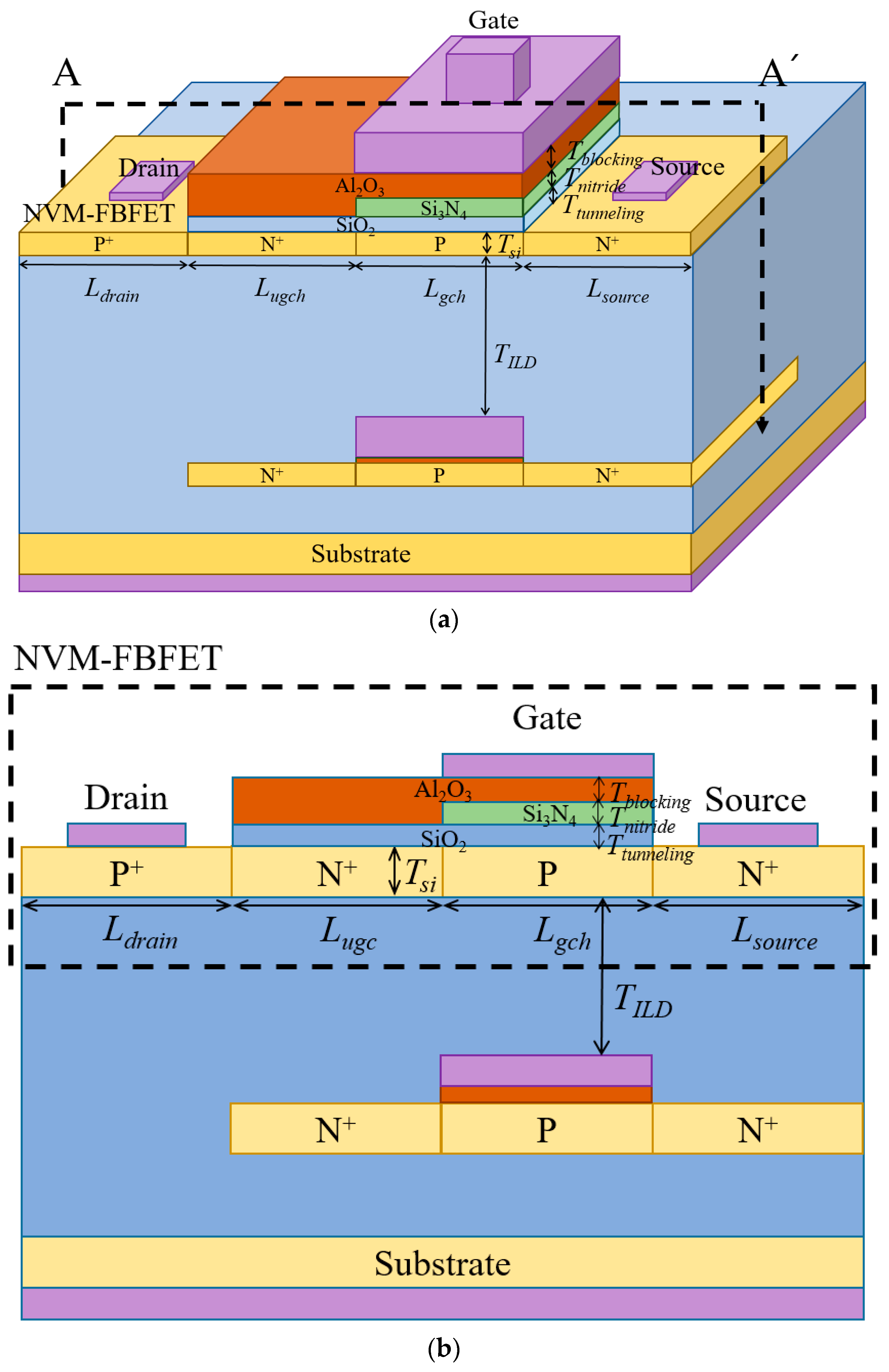
2. Simulation Structure and Parameters

Figure 1a,b show the 3D schematic and its cross-section of the A–A’ of the M3D-NVM-FBFET, respectively. The NVM-FBFET located in the top tier in the M3D-NVM-FBFET was benchmarked from the published paper [31]. The bottom tier of the M3D-NVM-FBFET is one fully depleted silicon-on-insulator (FD-SOI) metal–oxide–semiconductor field-effect transistor (MOSFET). The M3D-NVM-FBFET consists of the N-type FBFET (NFBFET) including the tunneling oxide–nitride–blocking oxide (ONO) stack. The NFBFET structure is basically configured with p-n-p-n structure. For the M3D structure, an FD-SOI FET structure is used for the NFBFET. This optimal structure of the NFBFET has been researched already [38], and the structure was used for this M3D-NVM-FBFET. The M3D-NVM-FBFET can be fabricated based on the elaboration step of previous work [39], and deposition of the ONO layer must be added before deposition of the gate material in the fabrication flow [40]. The materials of the ONO stack are SiO2, Si3N4, and Al2O3, and the thickness of each ONO layer is 4, 5, and 6 nm, respectively. The total length of the channel region is 100 nm, and the length of each gated and ungated channel region is 50 nm. The doping concentration of each drain, source, and the ungated channel region is 1 × 1020 cm−3, and that of the gated channel region is 1 × 1015 cm−3. These structure parameters are described in Table 1. The simulation was conducted using commercial TCAD simulator Atlas [41]. The physical models including SRH, CVT, FERMI, BGN, CONMOB, FLDMOB, CONSRH, and AUGER for the FBFET simulation and PF.NITRIDE for the NVM simulation were used.

3. Simulation Results

In this section, the simulation results of the M3D-NVM-FBFET will be discussed. First, the mechanism of the M3D-NVM-FBFET will be explained in Section 3.1. Then, the memory characteristics of the M3D-NVM-FBFET for programming, erasing, and retention will be discussed in Section 3.2. Finally, the electrical coupling for the M3D-NVM-FBFET will be discussed in Section 3.3.

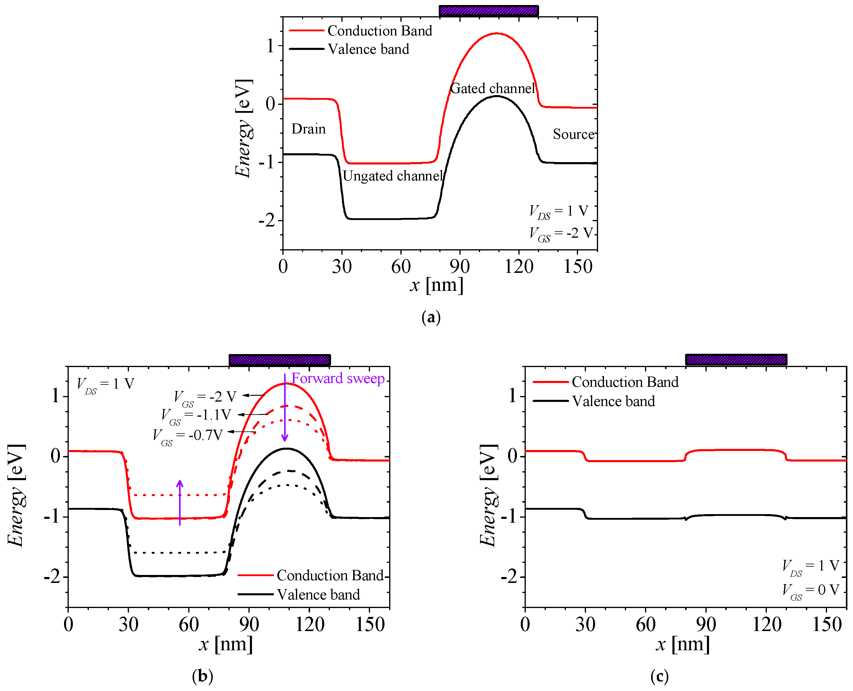
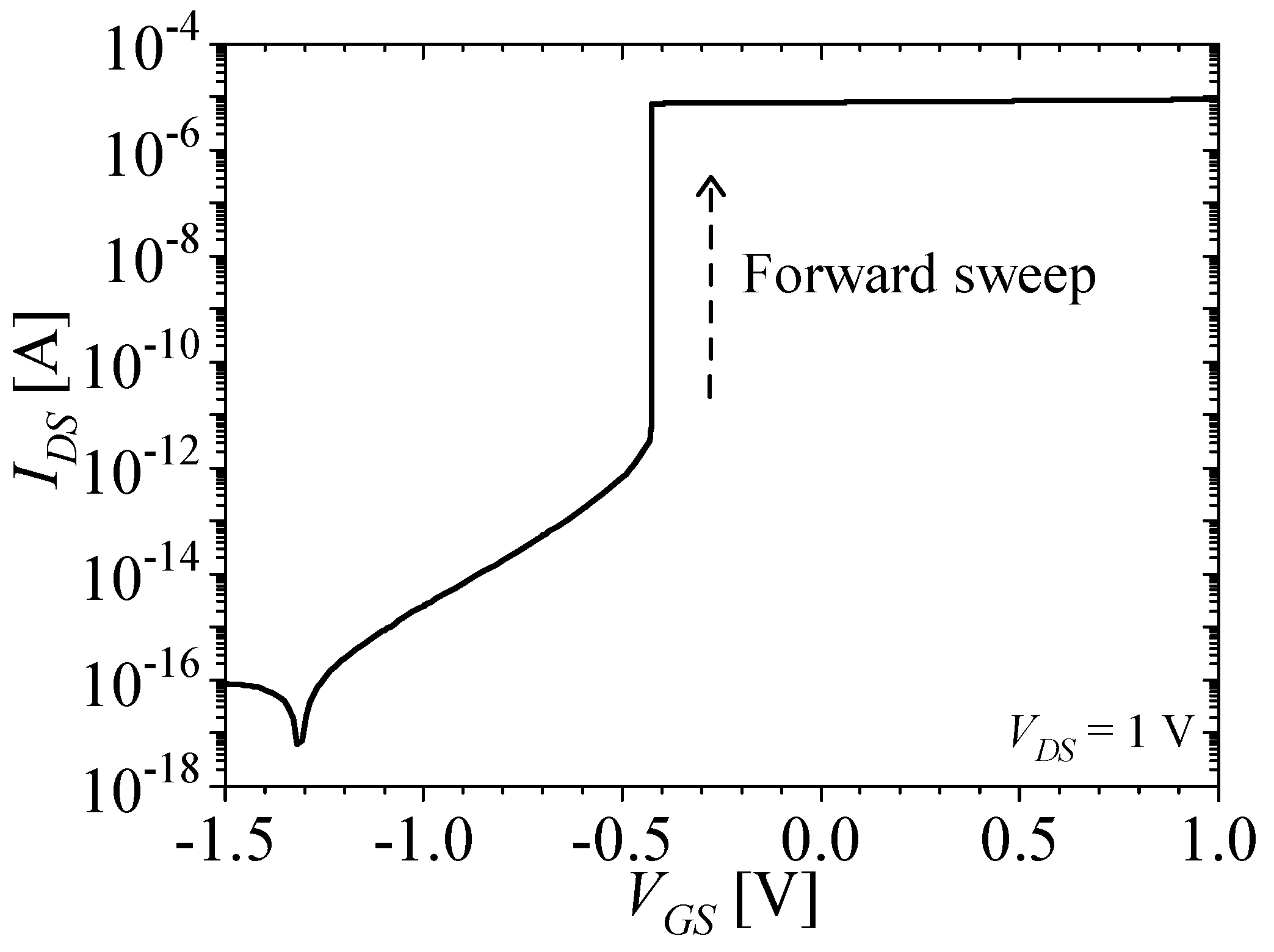
3.1. Mechanism of the M3D-NVM-FBFET

Figure 2a–c show the energy band of the off state, the forward sweep, and the on state of the M3D-NVM-FBFET, respectively. The black and red lines denote the valence band and the conduction band, respectively. Figure 3 shows the drain–source current (IDS)–gate–source voltage (VGS) characteristics of the M3D-NVM-FBFET with no charge in the nitride layer. For the off state of the M3D-NVM-FBFET, the drain–source voltage (VDS) and VGS are applied for 1 and −2 V, respectively. In this state, the carriers from the drain and source regions cannot inject into the channel region due to the potential barriers, as shown in Figure 2a. When the gate voltage starts the forward sweep at −2 V, the potential barrier in the gated channel region is lower, as shown in Figure 2b. Then, the electron from the source region can inject into the ungated channel region by thermionic emission. In the ungated channel region, the injected electrons accumulate and increase the carrier density. Subsequently, the potential barrier at the drain side is lower, so the hole from the drain region can diffuse into the ungated channel region. This positive feedback occurs through interaction between the electron and hole injection, as shown in Figure 2c. The positive feedback increases the current of the M3D-NVM-FBFET steeply, as shown in Figure 3. For the M3D-NVM-FBFET, the threshold voltage (VTH) is −0.43 V and the subthreshold swing is approximately zero.

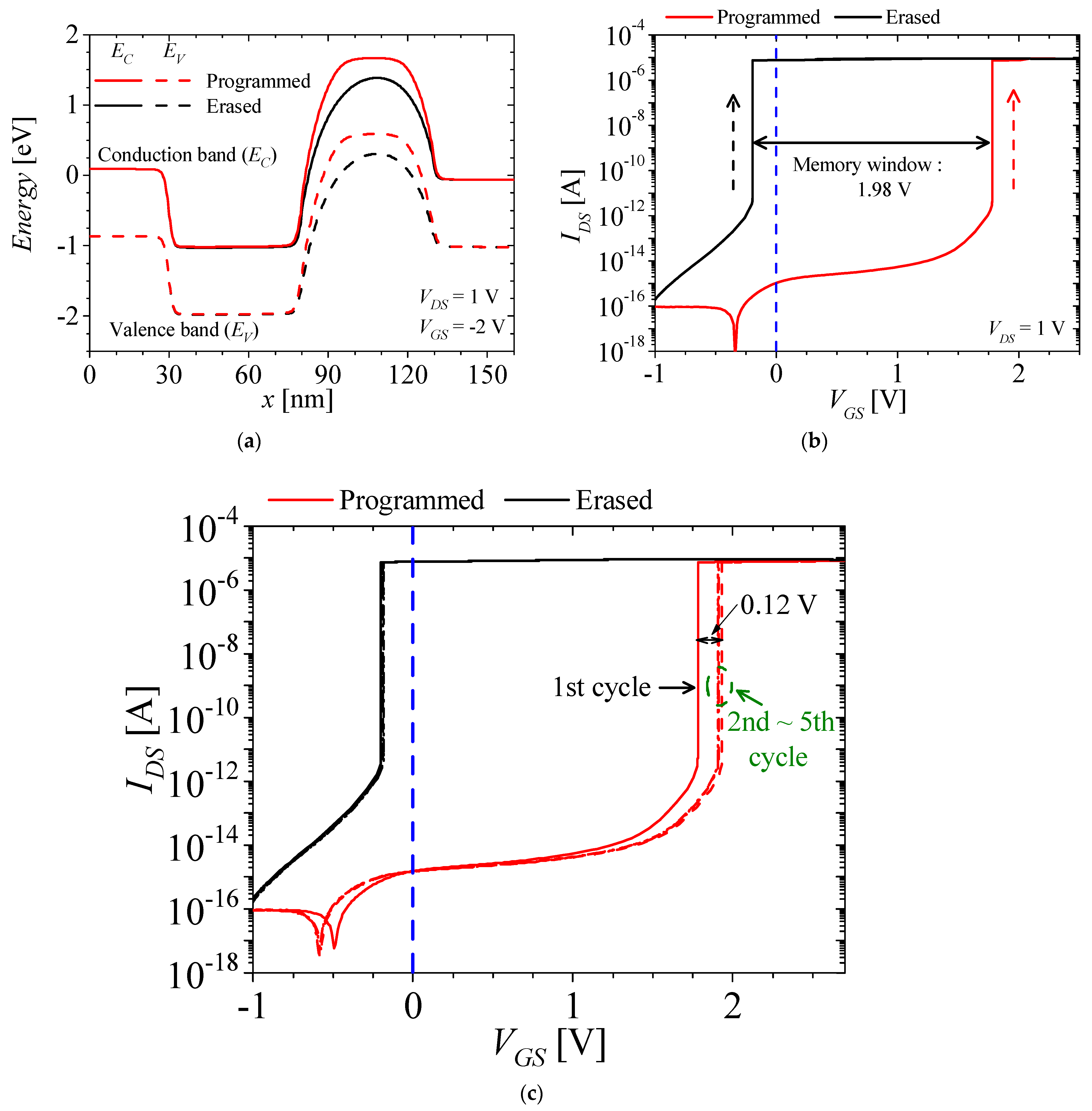
3.2. Memory Characteristics of the M3D-NVM-FBFET

Figure 4a,b show the energy band of the ONO layer and the trapped electron concentration in the nitride layer for the programming and erasing operations, respectively. The black, red, and blue lines denote the valence band, the conduction band, and the trapped electron concentration, respectively. To simulate the programming operation, trap parameters used in the simulation are described in Table 2. Those parameters are basically based on fitted data on the fabricated NVM devices [42,43,44,45]. In order to avoid degradation of the memory performance such as the hot carrier effect [46,47], the very high voltage was applied to the gate electrode utilizing Fowler–Nordheim (FN) tunneling and the drain voltage for read operation is relatively low (~1 V). For the memory operation, the programming and erasing voltages are 18 and −18 V, respectively. The programming and erasing times are 1 μs. When the programming voltage is applied at the gate, the high electric field directs the potential of the tunneling oxide narrow in the field direction. Then, the electron from the silicon body can be transported into the nitride layer by FN tunneling and trapping in the nitride layer. Moreover, the trapped electron in tunneling oxide can be transported by Poole–Frenkel emission, as shown in Figure 4a. For the erasing operation, the negative voltage is applied at the gate, and then the direction of the electric field is reversed compared to the programming operation. The trapped electrons from the nitride layer are emitted and transported into the silicon channel region by FN tunneling, as shown in Figure 4b.
Figure 5a–c show the energy band of the off state, IDSVGS characteristics of the M3D-NVM-FBFET after the programming and erasing operations, and IDSVGS characteristics of the M3D-NVM-FBFET after five cycles, respectively. The red and black lines denote the results after the programming and erasing operations, respectively. For the programming operation, the trapped electrons accumulate holes in the gated channel region. Then, the fermi-energy level of the gated channel region is lower and the potential barrier is higher. Therefore, in order to turn to the on state, higher VGS is required. For the erasing operation, the trapped electrons are eliminated, and then the raised barrier is lower, as shown in Figure 5a. After the programming operation, the VTH of the M3D-NVM-FBFET shifts to 1.78 V. Then, after the erasing operation, the VTH shifts from 1.78 to −0.2 V. For the M3D-NVM-FBFET, the memory window is 1.98 V, as shown in Figure 5b. After the first cycle, the VTH after the programming operation shifts from 1.78 to 1.9 V, and stays almost the same after 2~5 cycles, but one was not changed after the erasing operation, as shown in Figure 5c.
Figure 6 shows the retention characteristics of the M3D-NVM-FBFET. The red and black lines denote the change in the VTH for the M3D-NVM-FBFET after the programming and erasing operations, respectively. The retention simulation was conducted for 10 years (3 × 10⁸ s). The memory window of the M3D-NVM-FBFET decreased from 1.98 to 0.83 V, as shown in Figure 6, so that it operates as an NVM. Finally, the comparison of the memory performance for various NVM-FBFETs is summarized in Table 3. The M3D-NVM-FBFET demonstrate the same performance for the programming and erasing operation, but improvements in read time and retention characteristics are needed when compared to other NVM-FBFETs. However, only the M3D-NVM-FBFET structure is designed considering M3DI.

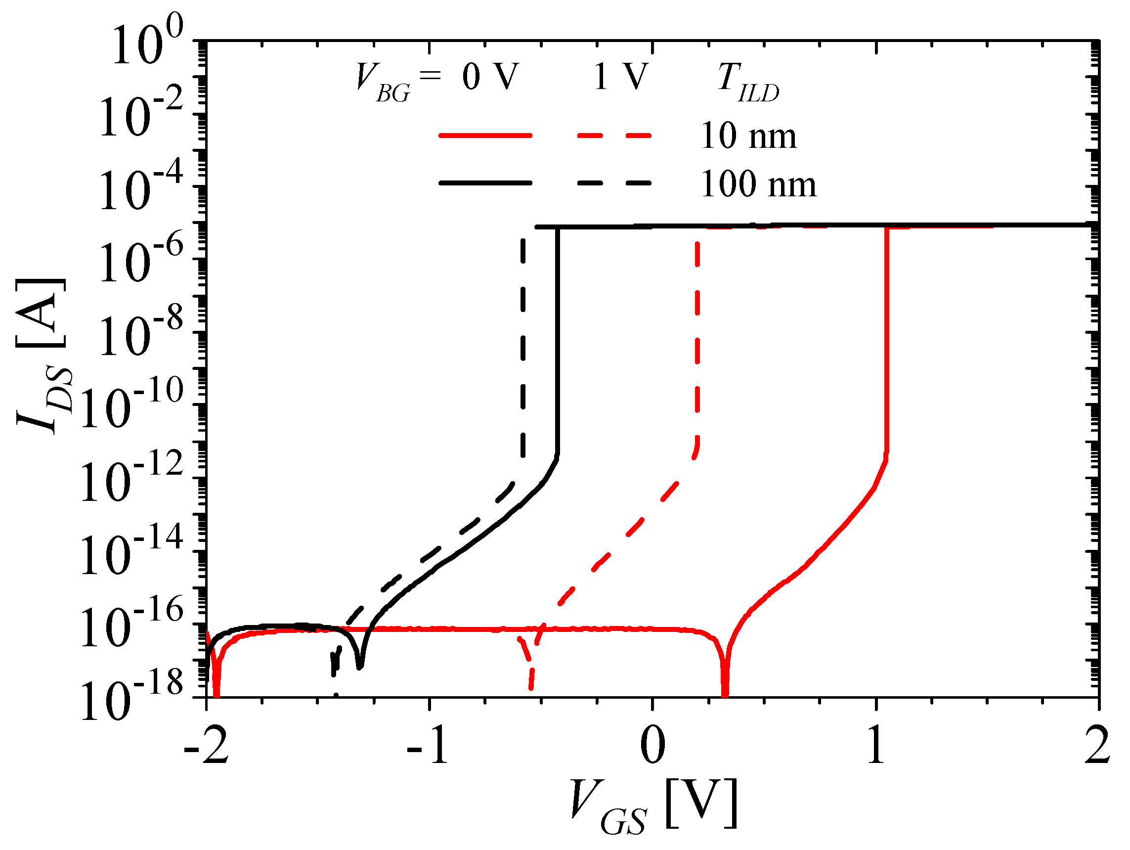
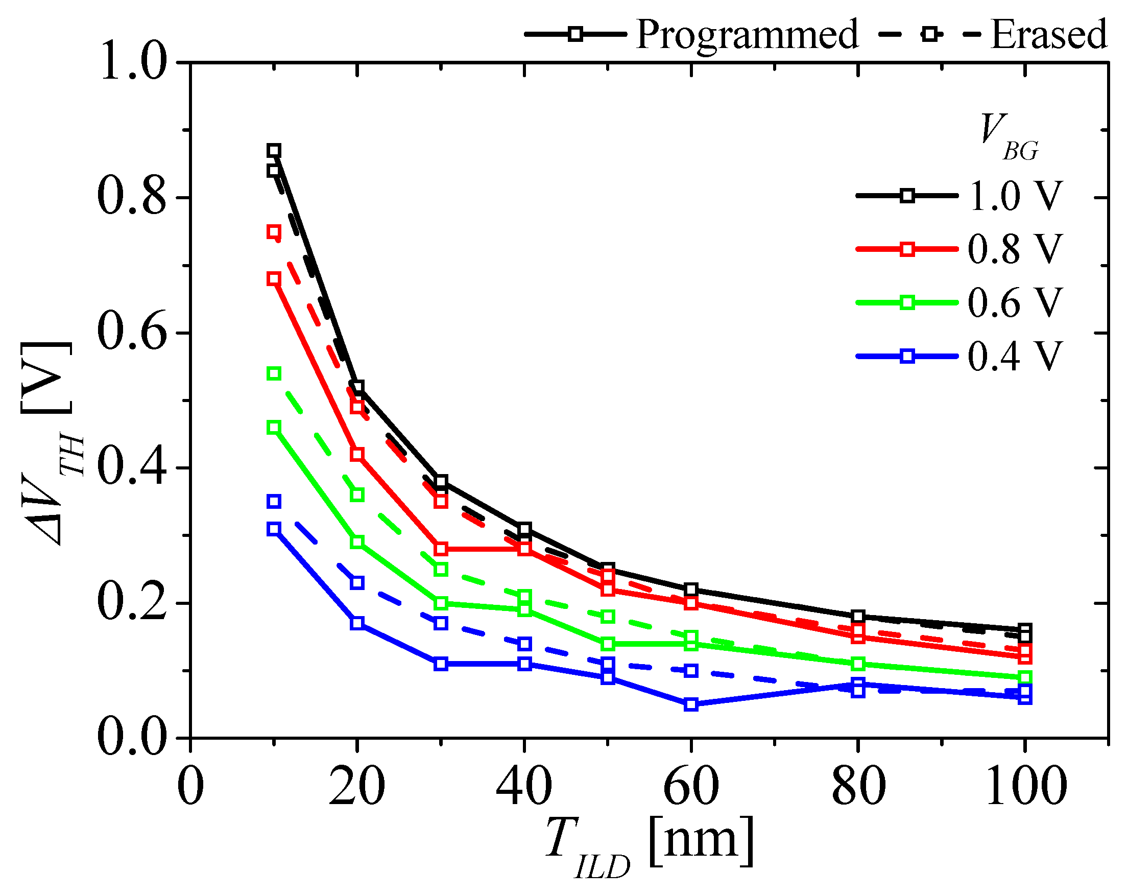
3.3. The Electrical Coupling Effect for the M3D-NVM-FBFET

Figure 7 shows the IDSVGS characteristics of the M3D-NVM-FBFET with no charge in the nitride layer at a thickness of the interlayer dielectric (TILD) of 10 and 100 nm at a bottom-gate voltage (VBG) of 0 and 1 V. The black and red lines denote those of a TILD of 10 and 100 nm, respectively, and the solid and dashed lines denote those of a VBG of 0 and 1 V, respectively. The electrical coupling for the M3D-NVM-FBFET is caused by the bottom-tier gate. When the VBG changes from 0 to 1 V, the VTH of the M3D-NVM-FBFET also changes, similar to the coupling effect of asymmetric double-gate FD-SOI [50] as follows:
Δ V T H T O N O T I L D ε I L D ε O N O Δ V B G ,
where ΔVTH represents the difference in the VTH when the VBG is changed by the ΔVBG, and TONO, εILD, and εONO represent the thickness of the ONO stack and the permittivity of the ILD and the ONO stack, respectively. Here, 1/εONO = 1/εblocking + 1/εnitride + 1/εtunneling, where εblocking, εnitride, and εtunneling are the permittivity of blocking oxide, nitride, and tunneling oxide, respectively. When the TILD decreases, the right-hand term of Equation (1) increases, then the ΔVTH increases, as shown in Figure 7. When the TILD is 100 and 10 nm, the ΔVTH is 0.16 and 0.84 V, respectively.
Figure 8 shows the change in the VTHVTH) for the M3D-NVM-FBFET with various TILD after programming and erasing operations, respectively. The solid and dashed lines denote the ΔVTH after the programming and erasing operations, respectively. The black, red, green, and blue lines denote the ΔVTH at VBG = 1, 0.8, 0.6, and 0.4 V, respectively. When the VBG is applied to the gate of the bottom transistor, the electric field is formed between the top and bottom transistors. Additionally, the magnitude of the field depends on the TILD and the VBG. As the TILD decreases and the VBG increases, the field is stronger, and the change in the VTH increases. When the TILD decreases from 100 to 10 nm, the ΔVTH after the programming and erasing operations increases from 0.16 to 0.87 V and from 0.15 to 0.84 V, respectively. When the VBG increases at TILD = 10 nm, the ΔVTH after the programming and erasing operations increases from 0.14 to 0.87 V and from 0.18 to 0.84 V. As the TILD decreases, the ΔVTH increases abruptly at a TILD of 50 nm. The electrical coupling must be considered below TILD = 50 nm before designing the M3D-NVM-FBFET.

4. Conclusions

In this study, the electrical characteristics and electrical coupling effect of the M3D-NVM-FBFET were investigated using TCAD. The M3D-NVM-FBFET is configured with a NVM-FBFET with and a MOSFET in the top and bottom tiers, respectively. For the M3D structure, the FD-SOI structure was used for the NFBFET and the MOSFET. For the memory operation, the programming and erasing voltages were applied at 18 and −18 V, respectively, and the programming and erasing time was 1 μs. The memory window of the M3D-NVM-FBFET was 1.98 V. As the retention simulation was conducted over 10 years, the memory window decreased from 1.98 to 0.83 V, but it can be operated as an NVM. For the M3D-NVM-FBFET, the electrical coupling is caused by the electric field from the bottom-tier transistor, and the magnitude of the field depends on the TILD and the VBG. When the TILD decreases, the ΔVTH after the programming and erasing operations changes from 0.16 to 0.87 V and from 0.15 to 0.84 V, respectively. When the VBG increases at TILD = 10 nm, the ΔVTH after the programming and erasing operations increases from 0.14 to 0.87 V and from 0.18 to 0.84 V. For the memory operation, the electrical coupling must be considered below TILD = 50 nm before designing the M3D-NVM-FBFET.

Author Contributions

Conceptualization, J.H.O. and Y.S.Y.; methodology, J.H.O. and Y.S.Y.; investigation, J.H.O. and Y.S.Y.; data curation, J.H.O.; writing—original draft preparation, J.H.O.; writing—review and editing, J.H.O. and Y.S.Y.; supervision, Y.S.Y.; project administration, Y.S.Y.; funding acquisition, Y.S.Y. All authors have read and agreed to the published version of the manuscript.

Funding

This research was supported by the Basic Science Research Program through NRF of Korea funded by the Ministry of Education (NRF-2019R1A2C1085295).

Acknowledgments

This work was supported by IDEC (EDA tool).

Conflicts of Interest

The authors declare no conflict of interest.

References

  1. Cavin, R.K.; Lugli, P.; Zhirnov, V.V. Science and Engineering Beyond Moore’s Law. Proc. IEEE 2012, 100, 1720–1749. [Google Scholar] [CrossRef]
  2. Frank, D.J.; Dennard, R.H.; Nowak, E.; Solomon, P.M.; Taur, Y.; Wong, H.-S.P. Device Scaling Limits of Si MOSFETs and Their Application Dependencies. Proc. IEEE 2001, 89, 259–288. [Google Scholar] [CrossRef]
  3. Clavelier, L.; Deguet, C.; Di Cioccio, L.; Augendre, E.; Brugere, A.; Gueguen, P.; Le Tiec, Y.; Moriceau, H.; Rabarot, M.; Signamarcheix, T.; et al. Engineered Substrates for Future More Moore and More than Moore Integrated Devices. In Proceedings of the 2010 International Electron Devices Meeting (IEDM), San Francisco, CA, USA, 6–8 December 2010; pp. 2.6.1–2.6.4. [Google Scholar]
  4. Grenouillet, L.; De Salvo, B.; Brunet, L.; Coignus, J.; Tabone, C.; Mazurier, J.; Le Royer, C.; Grosse, P.; Jaud, M.A.; Rivallin, P.; et al. Smart Co-Integration of Light Sensitive Layers with FDSOI Transistors for More than Moore Applications. In Proceedings of the 2014 SOI-3D-Subthreshold Microelectronics Technology Unified Conference (S3S), Millbrae, CA, USA, 6–9 October 2014; pp. 1–2. [Google Scholar]
  5. Hisamoto, D.; Lee, W.-C.; Kedzierski, J.; Takeuchi, H.; Asano, K.; Kuo, C.; Anderson, E.; King, T.-J.; Bokor, J.; Hu, C. FinFET-a Self-Aligned Double-Gate MOSFET Scalable to 20 nm. IEEE Trans. Electron Devices 2000, 47, 2320–2325. [Google Scholar]
  6. Singh, N.; Agarwal, A.; Bera, L.K.; Liow, T.Y.; Yang, R.; Rustagi, S.C.; Tung, C.H.; Kumar, R.; Lo, G.Q.; Balasubramanian, N.; et al. High-Performance Fully Depleted Silicon Nanowire (diameter/spl les/5 nm) Gate-All-around CMOS Devices. IEEE Electron Device Lett. 2006, 27, 383–386. [Google Scholar] [CrossRef]
  7. Ferhati, H.; Djeffal, F. Planar Junctionless Phototransistor: A Potential High-Performance and Low-Cost Device for Optical-Communications. Opt. Laser Technol. 2017, 97, 29–35. [Google Scholar] [CrossRef]
  8. Ferhati, H.; Djeffal, F. Boosting the Optical Performance and Commutation Speed of Phototransistor Using SiGe/Si/Ge Tunneling Structure. Mater. Res. Express 2018, 5, 065902. [Google Scholar] [CrossRef]
  9. Meguellati, M.; Djeffal, F. New Dual-Dielectric Gate All Around (DDGAA) RADFET Dosimeter Design to Improve the Radiation Sensitivity. Nucl. Instrum. Methods Phys. Res. Sect. A Accel. Spectrom. Detect. Assoc. Equip. 2012, 683, 24–28. [Google Scholar] [CrossRef]
  10. Yu, Y.S.; Najam, F. Compact Capacitance Model of L-Shape Tunnel Field-Effect Transistors for Circuit Simulation. J. Inf. Commun. Converg. Eng. 2021, 19, 263–268. [Google Scholar]
  11. Wong, S.; El-Gamal, A.; Griffin, P.; Nishi, Y.; Pease, F.; Plummer, J. Monolithic 3D Integrated Circuits. In Proceedings of the 2007 International Symposium on VLSI Technology, Systems and Applications (VLSI-TSA), Hsinchu, Taiwan, 23–25 April 2007; pp. 1–4. [Google Scholar]
  12. Vinet, M.; Batude, P.; Fenouillet-Beranger, C.; Clermidy, F.; Brunet, L.; Rozeau, O.; Hartmannn, J.; Billoint, O.; Cibrario, G.; Previtali, B.; et al. Monolithic 3D Integration: A Powerful Alternative to Classical 2D Scaling. In Proceedings of the 2014 SOI-3D-Subthreshold Microelectronics Technology Unified Conference (S3S), Millbrae, CA, USA, 6–9 October 2014; pp. 1–3. [Google Scholar]
  13. Batude, P.; Vinet, M.; Pouydebasque, A.; Le Royer, C.; Previtali, B.; Tabone, C.; Hartmann, J.-M.; Sanchez, L.; Baud, L.; Carron, V.; et al. 3D Monolithic Integration. In Proceedings of the 2011 IEEE International Symposium of Circuits and Systems (ISCAS), Rio de Janeiro, Brazil, 15–18 May 2011; pp. 2233–2236. [Google Scholar]
  14. Bishop, M.D.; Wong, H.-S.P.; Mitra, S.; Shulaker, M.M. Monolithic 3-D Integration. IEEE Micro 2019, 39, 16–27. [Google Scholar] [CrossRef]
  15. Lee, G.J.; Ahn, T.J.; Lim, S.K.; Yu, Y.S. Investigation into electrical characteristics of logic circuit consisting of modularized mon-olithic 3D inverter unit cell. J. Inf. Commun. Converg. Eng. 2022, 20, 137–142. [Google Scholar]
  16. Nayak, D.K.; Banna, S.; Samal, S.K.; Lim, S.K. Power, Performance, and Cost Comparisons of Monolithic 3D ICs and TSV-Based 3D ICs. In Proceedings of the 2015 IEEE SOI-3D-Subthreshold Microelectronics Technology Unified Conference (S3S), Rohnert Park, CA, USA, 5–8 October 2015; pp. 1–2. [Google Scholar]
  17. Ebrahimi, M.S.; Hills, G.; Sabry, M.M.; Shulaker, M.M.; Wei, H.; Wu, T.F.; Mitra, S.; Wong, H.-S.P. Monolithic 3D Integration Advances and Challenges: From Technology to System Levels. In Proceedings of the 2014 SOI-3D-Subthreshold Microelectronics Technology Unified Conference (S3S), Millbrae, CA, USA, 6–9 October 2014; pp. 1–2. [Google Scholar]
  18. Lee, S.-Y.; Park, J. Architecture of 3D Memory Cell Array on 3D IC. In Proceedings of the 2012 4th IEEE International Memory Workshop, Milan, Italy, 20–23 May 2013; pp. 1–3. [Google Scholar]
  19. Lee, S.-Y.; Schroder, D.K. 3D IC Architecture for High Density Memories. In Proceedings of the 2010 IEEE International Memory Workshop, Seoul, Republic of Korea, 16–19 May 2010; pp. 1–6. [Google Scholar]
  20. Padilla, A.; Yeung, C.W.; Shin, C.; Hu, C.; King Liu, T.-J. Feedback FET: A Novel Transistor Exhibiting Steep Switching Behavior at Low Bias Voltages. In Proceedings of the 2008 IEEE International Electron Devices Meeting (IEDM), San Francisco, CA, USA, 15–17 December 2008; pp. 1–4. [Google Scholar]
  21. Dirani, H.E.; Solaro, Y.; Fonteneau, P.; Ferrari, P.; Cristoloveanu, S. Sharp-Switching Z2-FET Device in 14 nm FDSOI Technology. In Proceedings of the 2015 45th European Solid State Device Research Conference (ESSDERC), Graz, Austria, 14–18 September 2015; pp. 250–253. [Google Scholar]
  22. Lee, K.H.; Dirani, H.E.; Fonteneau, P.; Bawedin, M.; Sato, S.; Cristoloveanu, S. Sharp Switching, Hysteresis-Free Characteristics of Z2-FET for Fast Logic Applications. In Proceedings of the 2018 48th European Solid-State Device Research Conference (ESSDERC), Dresden, Germany, 3–6 September 2018; pp. 74–77. [Google Scholar]
  23. Kwon, M.-W.; Hwang, S.; Baek, M.-H.; Cho, S.; Park, B.-G. Dual Gate Positive Feedback Field-Effect Transistor for Low Power Analog Circuit. In Proceedings of the 2017 Silicon Nanoelectronics Workshop (SNW), Kyoto, Japan, 4–5 June 2017; pp. 115–116. [Google Scholar]
  24. Lee, C.; Ko, E.; Shin, C. Steep Slope Silicon-On-Insulator Feedback Field-Effect Transistor: Design and Performance Analysis. IEEE Trans. Electron Devices 2019, 66, 286–291. [Google Scholar] [CrossRef]
  25. Suddarsi, S.K.; Dhanaraj, K.J.; Saramekala, G.K. Investigation of Switching and Inverter Characteristics of Recessed-Source/Drain (Re–S/D) Silicon-on-Insulator (SOI) Feedback Field Effect Transistor (FBFET). Microelectron. J. 2023, 138, 105855. [Google Scholar] [CrossRef]
  26. Cho, J.; Lim, D.; Woo, S.; Cho, K.; Kim, S. Static Random Access Memory Characteristics of Single-Gated Feedback Field-Effect Transistors. IEEE Trans. Electron Devices 2019, 66, 413–419. [Google Scholar] [CrossRef]
  27. Woo, S.; Cho, J.; Lim, D.; Cho, K.; Kim, S. Transposable 3T-SRAM Synaptic Array Using Independent Double-Gate Feedback Field-Effect Transistors. IEEE Trans. Electron Devices 2019, 66, 4753–4758. [Google Scholar] [CrossRef]
  28. Parihar, M.S.; Lee, K.H.; El Dirani, H.; Navarro, C.; Lacord, J.; Martinie, S.; Barbe, J.-C.; Fonteneau, P.; Galy, P.; Le Royer, C.; et al. Low-Power Z2-FET Capacitorless 1T-DRAM. In Proceedings of the 2017 IEEE International Memory Workshop (IMW), Monterey, CA, USA, 14–17 May 2017; pp. 1–4. [Google Scholar]
  29. Kwon, M.-W.; Park, K.; Baek, M.-H.; Lee, J.; Park, B.-G. A Low-Energy High-Density Capacitor-Less I&F Neuron Circuit Using Feedback FET Co-Integrated with CMOS. IEEE J. Electron Devices Soc. 2019, 7, 1080–1084. [Google Scholar]
  30. Woo, S.; Cho, J.; Lim, D.; Park, Y.-S.; Cho, K.; Kim, S. Implementation and Characterization of an Integrate-and-Fire Neuron Circuit Using a Silicon Nanowire Feedback Field-Effect Transistor. IEEE Trans. Electron Devices 2020, 67, 2995–3000. [Google Scholar] [CrossRef]
  31. Kang, H.; Cho, J.; Kim, Y.; Lim, D.; Woo, S.; Cho, K.; Kim, S. Nonvolatile and Volatile Memory Characteristics of a Silicon Nanowire Feedback Field-Effect Transistor with a Nitride Charge-Storage Layer. IEEE Trans. Electron Devices 2019, 66, 3342–3348. [Google Scholar] [CrossRef]
  32. Spessot, A.; Oh, H. 1T-1C Dynamic Random Access Memory Status, Challenges, and Prospects. IEEE Trans. Electron Devices 2020, 67, 1382–1393. [Google Scholar] [CrossRef]
  33. Lee, J.C.; Kim, J.; Kim, K.W.; Ku, Y.J.; Kim, D.S.; Jeong, C.; Yun, T.S.; Kim, H.; Cho, H.S.; Oh, S.; et al. High Bandwidth Memory (HBM) with TSV Technique. In Proceedings of the 2016 International SoC Design Conference (ISOCC), Jeju, Republic of Korea, 23–26 October 2016; pp. 181–182. [Google Scholar]
  34. Yu, Y.S.; Panth, S.; Lim, S.K. Electrical Coupling of Monolithic 3-D Inverters. IEEE Trans. Electron Devices 2016, 63, 3346–3349. [Google Scholar] [CrossRef]
  35. Ahn, T.J.; Perumal, R.; Lim, S.K.; Yu, Y.S. Parameter Extraction and Power/Performance Analysis of Monolithic 3-D Inverter (M3INV). IEEE Trans. Electron Devices 2019, 66, 1006–1011. [Google Scholar] [CrossRef]
  36. Ahn, T.-J.; Yu, Y.S.; Kim, N.H. Comparison of Two-Types of Monolithic 3D Inverter Consisting of MOSFETs and Junctionless FETs. In Proceedings of the 2020 International Conference on Electronics, Information, and Communication (ICEIC), Barcelona, Spain, 19–22 January 2020; pp. 1–3. [Google Scholar]
  37. Ahn, T.J.; Yu, Y.S. Circuit Simulation Considering Electrical Coupling in Monolithic 3D Logics with Junctionless FETs. Micromachines 2020, 11, 887. [Google Scholar] [CrossRef] [PubMed]
  38. Oh, J.H.; Yu, Y.S. Investigation of Monolithic 3D Integrated Circuit Inverter with Feedback Field Effect Transistors Using TCAD Simulation. Micromachines 2020, 11, 852. [Google Scholar] [CrossRef] [PubMed]
  39. Oh, J.H.; Yu, Y.S. A Monolithic 3-Dimensional Static Random Access Memory Containing a Feedback Field Effect Transistor. Micromachines 2022, 13, 1625. [Google Scholar] [CrossRef]
  40. Hwang, J.-R.; Lee, T.-L.; Ma, H.-C.; Lee, T.-C.; Chung, T.-H.; Chang, C.-Y.; Liu, S.-D.; Perng, B.-C.; Hsu, J.-W.; Lee, M.-Y.; et al. 20nm Gate Bulk-finFET SONOS Flash. In Proceedings of the IEEE International Electron Devices Meeting, 2005, IEDM Technical Digest, Washington, DC, USA, 5 December 2005; pp. 154–157. [Google Scholar]
  41. Silvaco Int. ATLAS Ver. 5. 32. 1. R Manual; Silvaco Int.: Santa Clara, CA, USA, 2022. [Google Scholar]
  42. Nowak, E.; Hubert, A.; Perniola, L.; Ernst, T.; Ghibaudo, G.; Reimbold, G.; De Salvo, B.; Boulanger, F. In-Depth Analysis of 3D Silicon Nanowire SONOS Memory Characteristics by TCAD Simulations. In Proceeding of the 2010 IEEE International Memory Workshop, Seoul, Republic of Korea, 16–19 May 2010; pp. 1–4. [Google Scholar]
  43. Paul, A.; Sridhar, C.; Gedam, S.; Mahapatra, S. Comprehensive Simulation of Program, Erase and Retention in Charge Trapping Flash Memories. In Proceedings of the 2006 International Electron Devices Meeting (IEDM), San Francisco, CA, USA, 11–13 December 2006; pp. 1–4. [Google Scholar]
  44. Bachhofer, H.; Reisinger, H.; Bertagnolli, E.; von Philipsborn, H. Transient Conduction in Multidielectric Silicon–Oxide–Nitride–Oxide Semiconductor Structures. J. Appl. Phys. 2001, 89, 2791–2800. [Google Scholar] [CrossRef]
  45. Vianello, E.; Driussi, F.; Arreghini, A.; Palestri, P.; Esseni, D.; Selmi, L.; Akil, N.; van Duuren, M.J.; Golubovic, D.S. Experimental and Simulation Analysis of Program/Retention Transients in Silicon Nitride-Based NVM Cells. IEEE Trans. Electron Devices 2009, 56, 1980–1990. [Google Scholar] [CrossRef]
  46. Bentrcia, T.; Djeffal, F.; Benhaya, A.H. Continuous Analytic I-V Model for GS DG MOSFETs Including Hot-Carrier Degradation Effects. J. Semicond. 2012, 33, 014001. [Google Scholar] [CrossRef]
  47. Djeffal, F.; Bentrcia, T.; Abdi, M.A.; Bendib, T. Drain Current Model for Undoped Gate Stack Double Gate (GSDG) MOSFETs Including the Hot-Carrier Degradation Effects. Microelectron. Reliab. 2011, 51, 550–555. [Google Scholar] [CrossRef]
  48. ITRS. 2013. Available online: http://www.itrs2.net/2013-itrs.html (accessed on 1 September 2023).
  49. Han, S.; Kim, Y.; Son, D.; Baac, H.W.; Won, S.M.; Shin, C. Study on Memory Characteristics of Fin-Shaped Feedback Field Effect Transistor. Semicond. Sci. Technol. 2022, 37, 065006. [Google Scholar] [CrossRef]
  50. Ernst, T.; Cristoloveanu, S.; Ghibaudo, G.; Ouisse, T.; Horiguchi, S.; Ono, Y.; Takahashi, Y.; Murase, K. Ultimately Thin Double-Gate SOI MOSFETs. IEEE Trans. Electron Devices 2003, 50, 830–838. [Google Scholar] [CrossRef]
Figure 1. (a) A 3-dimensional schematic of the M3D-NVM-FBFET; (b) its cross-section of A–A’.
Micromachines 14 01822 g001
Figure 2. The energy band of the M3D-NVM-FBFET for (a) the off state (VDS = 1 V and VGS = −2 V), (b) the forward sweep at different VGS (VDS = 1 V), and (c) the on state (VDS = 1 V and VGS = 0 V).
Micromachines 14 01822 g002
Figure 3. IDSVGS characteristics of the M3D-NVM-FBFET with no charge in the nitride layer (VDS = 1 V).
Micromachines 14 01822 g003
Figure 4. Energy band of the ONO layer and the trapped electron concentration in the nitride layer for (a) programming (VGS = 18 V) and (b) erasing operations (VGS = −18 V).
Micromachines 14 01822 g004
Figure 5. (a) Energy band in the off state (VDS = 1 V and VGS = −2 V), (b) IDSVGS characteristics of the M3D-NVM-FBFET (VDS = 1 V) after the programming operation (red line) and the erasing operation (black line), and (c) IDSVGS characteristics of the M3D-NVM-FBFET after five cycles.
Micromachines 14 01822 g005
Figure 6. Retention characteristics of the M3D-NVM-FBFET for 10 years.
Micromachines 14 01822 g006
Figure 7. IDSVGS characteristics of the M3D-NVM-FBFET with no charge in the nitride layer at TILD = 10 and 100 nm at VBG = 0 and 1 V.
Micromachines 14 01822 g007
Figure 8. Change in the VTH for the M3D-NVM-FBFET with various TILD after the programming (solid line) and erasing (dashed line) operations as a VBG of for 1.0 (black), 0.8 (red), 0.6 (green), and 0.4 V (blue) is applied.
Micromachines 14 01822 g008
Table 1. Structure parameters of the M3D-NVM-FBFET.
ParametersDescriptionValue/Unit
Ldrain, LsourceLength of the drain and source regions30 nm
LugchLength of the ungated channel region50 nm
LgchLength of the gated channel region50 nm
TblockingThickness of the blocking oxide layer (Al2O3)6 nm
TnitrideThickness of the nitride layer (Si3N4)5 nm
TtunnelingThickness of the tunneling oxide layer (SiO2)4 nm
TsiThickness of the silicon body6 nm
TILDThickness of the interlayer dielectric (ILD)Var.
Ndrain, NsourceDoping concentration of the drain and source regions1 × 1020 cm−3
NugchDoping concentration of the ungated channel region1 × 1020 cm−3
NgchDoping concentration of the gated channel region1 × 1015 cm−3
ΦFBFETWork function of the gate metal5.3 eV
Table 2. Trap parameters for the nitride layer for the M3D-NVM-FBFET.
ParameterValue/Unit
Trap energy level1.2 eV
Effective mass electron, me*0.33 m0
Effective mass hole, mh*0.46 m0
Capture cross-section1 × 10−13 cm2
Trap density1 × 1020 cm−3
Table 3. Comparison of the memory performance for various NVM-FBFETs.
NVM DevicesProgram TimeErase TimeRead TimeMonolithic 3D Integration
NOR Flash [48]1 μs1 ms15 nsX
NW NVM-FBFET [31]1 μs1 μs200 nsX
FinFET NVM-FBFET [49]1 μs1 μs10 nsX
This work1 μs1 μs~100 nsO
Disclaimer/Publisher’s Note: The statements, opinions and data contained in all publications are solely those of the individual author(s) and contributor(s) and not of MDPI and/or the editor(s). MDPI and/or the editor(s) disclaim responsibility for any injury to people or property resulting from any ideas, methods, instructions or products referred to in the content.

