Abstract
Flip chip bonding technology on gold–tin (Au-Sn) microbumps for MEMS (Micro Electro Mechanical Systems) and 3D packaging is becoming increasingly important in the electronics industry. The main advantages of Au-Sn microbumps are a low electrical resistance, high electrical reliability, and fine pitch. However, the bonding temperature is relatively high, and the forming mechanism of an intermetallic compound (IMC) is complicated. In this study, Au-Sn solid-state diffusion (SSD) bonding is performed using the thermal gradient bonding (TGB) method, which lowers bonding temperature and gains high bonding strength in a short time. Firstly, Au-Sn microbumps with a low roughness are prepared by using an optimized process. Then, Au-Sn bonding parameters including bonding temperature, bonding time, and bonding pressure are optimized to obtain a higher bonding quality. The shear strength of 23.898 MPa is obtained when bonding in the HCOOH environment for 10 min at the gradient temperature of 150 °C/250 °C with a bonding pressure of more than 10 MPa. The IMC of Au-Sn is found to be Au-Sn and Au5Sn. The effect of annealing time on the IMC is also investigated. More and more Au5Sn is generated with an increase in annealing time, and Au5Sn is formed after Sn is depleted. Finally, the effect of annealing time on the IMC is verified by using finite element simulation, and the bonding strength of IMC was found to be higher when the bonding temperature is 150 °C at the cold side and 250 °C at the hot side. The temperature in the bonding area can reach 200 °C, which proves that the Au-Sn bonding process is solid-state diffusion because the temperature gradient reaches 2500 °C/cm.
1. Introduction
In recent years, the electronics industry has witnessed a surging demand for microbump flip-chip interconnections, driven by the miniaturization and portability demand of electronic products [1,2]. This brings several challenges such as smaller pitch bonding and higher overall reliability [3,4]. Au-Sn microbump bonding emerges as a prominent candidate due to Au-Sn intermetallic compounds (IMC) offering superior mechanical properties, lower electrical conductivity, and higher thermal conductivity [5,6,7]. Bonding techniques for Au-Sn microbumps encompass eutectic bonding and solid–liquid interdiffusion (SLID) bonding. Eutectic bonding technology is widely used due to its low bonding pressure and capacity for high-density integration [8,9,10,11,12,13].
Traditionally, the Au-Sn eutectic bonding process proceeds at the temperature range of 280 °C–350 °C [14,15], involving solid–liquid diffusion bonding or instantaneous liquid-phase bonding. However, this method carries the risk of Sn extrusion, leading to potential short-circuits [16,17]. Additionally, the high bonding temperature engenders significant residual thermal stress, weakening the module and device reliability [18]. Lower bonding temperatures prolong bonding times, decrease productivity, escalate process costs, and introduce bonding quality issues, which limits applicability in multi-chip interconnection. High temperatures increase Sn oxidation, necessitating special environments like H2, HCOOH, or vacuum during bonding [19].
To circumvent the challenges posed by high temperatures, solid-state diffusion bonding techniques at lower temperatures have gained attraction. These techniques typically operate below the melting point of Sn (231.89 °C) [20]. Noteworthy research by the University of Tokyo explores low-temperature solid-state Au-Sn bonding, leveraging the surface-activated bonding (SAB) method to bond 30 µm pitch Au-Sn microbumps in ambient air SAB [21]. Nevertheless, certain aspects related to reliability remain to be elucidated. In a series of studies, a team from National Taiwan University discovered a temperature gradient bonding method to expedite the diffusion between Cu-Sn atoms, reducing bonding time and enhancing production efficiency [22]. To mitigate surface oxide issues on Sn bumps, the team from Osaka University achieved high-quality, low-temperature solid-state Cu-Sn bonding by introducing HCOOH vapor under specific conditions (200 °C, 20 MPa, and 20 min). Remarkably, shear strengths of samples bonded in an HCOOH environment surpassed those bonded in an N2 environment [23,24]. The team at Tsinghua University investigated the low-temperature Cu/Sn/Cu solid-state diffusion (SSD) bonding technique by treating the microbumps with Ar (5% H2) plasma and obtained an average bond strength of 5 MPa after bonding at 200 °C for 60 min at a bonding pressure of 6.7 MPa [25]. Few studies about Au-Sn bonding at lower temperatures are found.
This study harnesses lower-temperature, high-quality, and narrow-pitch Au-Sn bonding by the mechanism of solid-state diffusion. To lower the bonding temperature, Au-Sn microbump quality is first optimized by the electroplating and evaporative deposition processes. A pretreatment method is employed to eliminate surface oxides from the microbumps before bonding. Subsequently, a temperature gradient method in an HCOOH environment is applied and validated in the Au-Sn microbump bonding with a pitch of 20 µm. Finite element simulations corroborate that the bonding process involves solid-state diffusion in the temperature gradient bonding. Through the integration of simulation and experiment, the objective is to provide insights into the rapid low-temperature Au-Sn bonding process and optimize bonding parameters for prospective microelectronic packaging applications.
2. Materials and Methods
2.1. Preparation of Microbump and Bonded Chip
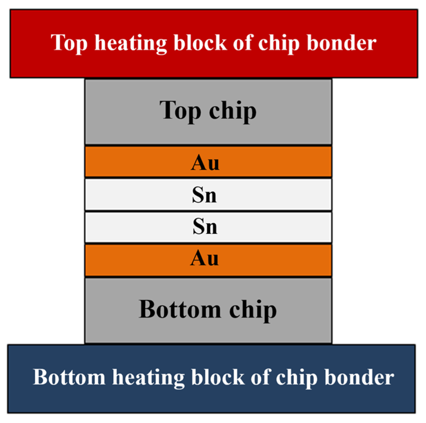
The bonding structure of Au-Sn microbumps is illustrated in Figure 1, featuring the Au/Sn-Sn/Au sandwich structure of the bumps. The Au bumps are dimensionally congruent with the Sn bumps, with a size of 10 × 10 µm. Heat conduction through the top and bottom ceramic heating blocks facilitates isothermal heating. Alternatively, a temperature gradient can be formed by maintaining different temperatures at the top and bottom heating blocks.
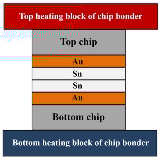
Figure 1.
Temperature gradient bonding (TGB) structure.
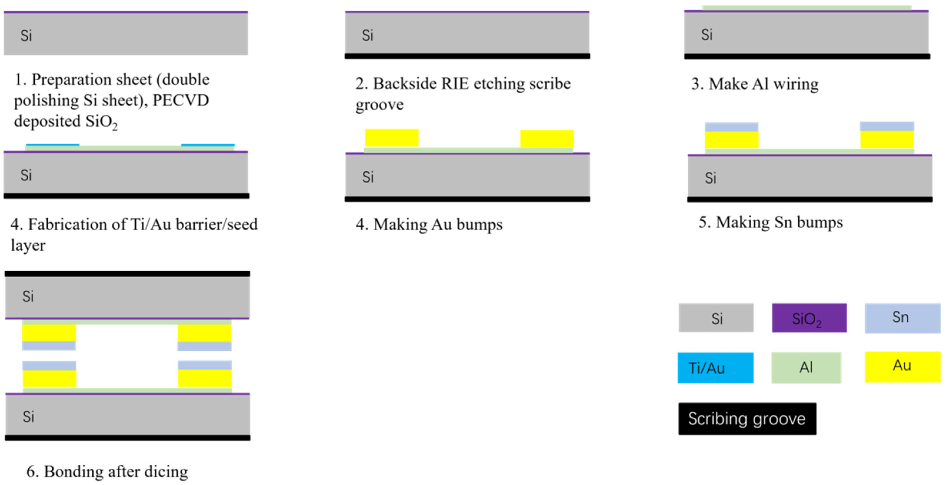
In this study, the process was initiated by creating scribe grooves and alignment marks on the backside of a 550 mm thick double-throw silicon oxide wafer by Reactive ion etching. This step is essential for facilitating subsequent alignment bonding. Then, an Al metal layer with a thickness of 1 µm was deposited by sputtering and etched by the wetting process. The Au/Sn microbumps were then fabricated by an electroplating and evaporation process, respectively. The Au/Sn microbumps had a thickness of 4 µm/2 µm. Subsequently, wafers were sliced into a bottom bonding chip with 1.2 cm × 1.2 cm and a top bonding chip with 1 cm × 1 cm. These chips were placed on the bonding equipment for pre-bonding experiments, as illustrated in Figure 2.

Figure 2.
Bonded chip manufacturing flowchart.
The bonding parameter optimization was conducted by changing the bonding time, bonding pressure, and bonding temperature. The bonding was carried out using an FC150 (SUSS MicroTec is located in Garching, Germany). After bonding, the shear strength of interconnecting bumps on the bonded chips was assessed on a shear force tester. To observe the IMC, the cross-sectional sample was prepared by an EcoMet30 (Buehler is based in Lake Bluff) grinding and polishing machine (diamond polishing disk roughness ~0.05 µm) and a Leica EM TIC 3X (Leica Microsystems in Vizsla, Germany) triple-ion beam dicing machine. Finally, we characterized the microstructure of the IMC through scanning electron microscopy (GeminiSEM 300, ZEISS in Oberkochen, Germany) combined with chemical analysis by an EDS energy spectrometer.
2.2. Bonding Temperature Distribution Simulation
To reveal the temperature distribution at the bonding interface and uncover the thermal diffusion mechanism, finite element simulation was investigated using COMSOL in both isothermal bonding and temperature gradient bonding [26,27,28,29]. The bonding model is the same as the bonding structure in Figure 1. For heat transfer analysis, engineering problems involving heat flow rate and temperature parameters in the structure are typically assessed. The nonlinear flow equation is usually expressed as below [30]:
where, K represents the conduction matrix encompassing the heat conduction, radiation rate, convection coefficient, and shape coefficient. {T} signifies the temperature vector for each computing node, [C] stands for the fixed specific heat capacity matrix, and {Q} represents the heat flow rate load vector. By examining changes in heat flux caused by variations in the system’s temperature field over time, the temperature field was analyzed at a constant temperature, which was maintained during steady-state conditions. At this stage, the system attained equilibrium, with heat inflow and generation equaling heat outflow. Under these conditions, the heat flow equation is simplified as {Q} = [K]{T}.
Heat transfer takes place through three mechanisms: heat convection, heat radiation, and heat diffusion. Thermal diffusion, particularly involved in this study, means the transfer of heat from regions of higher temperature to those with lower temperature due to a temperature gradient. This diffusion process is controlled by Fourier’s law [31]:
where k represents thermal conductivity (W/(m·K)), and A is the thermal conductivity area (m2).
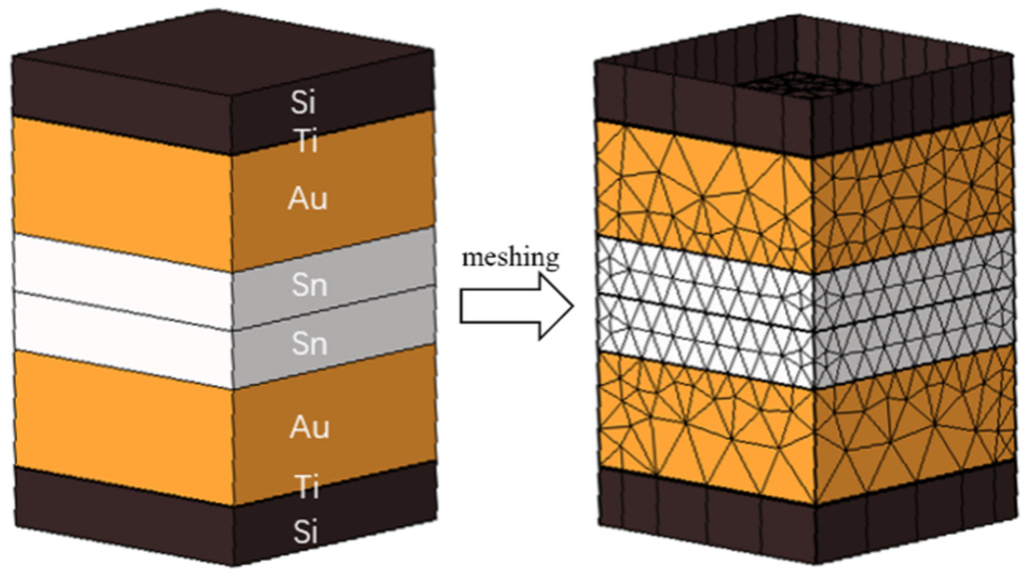
As depicted in Figure 3, the simulation modeling is based on the actual size of the microbumps. The silicon oxide layer, seed layer, and Al wiring layer were excluded because the focus was on simulating the heating device in the bonding process by applying temperatures at the ends of the top and bottom Si sheets. This study employed mesh delineation to create the model.

Figure 3.
Locally bonded model and meshed model.
3. Results and Discussion
In this work, several bonding parameters were firstly proposed to optimize a set of bonding parameters under TGB bonding technology. Then, the comparison between thermal gradient bonding and isothermal bonding was performed to derive the underlying reason for the higher strength. Then, the finite element simulation method was further proposed to verify the conclusion and confirm the TGB bonding belonging to solid diffusion. At last, the IMC evolution was investigated to uncover the stable IMC phase, which is important when applied for high-power device interconnection.
3.1. Bonding Parameter Optimization
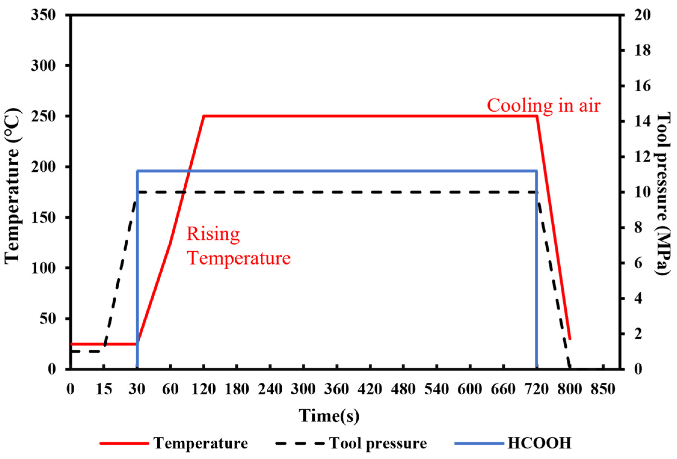
To achieve the robust chip-scale Au-Sn bonding with a low temperature, short time and high bonding strength, preliminary tuning of the pre-bonding parameters, including the bonding time, temperature and pressure, was performed under the HCOOH treatment condition. Several sets of parameters were tested, including the bonding time of 5, 10, and 20 min, the bonding pressures of 5, 10, and 20 MPa, and the gradient bonding temperature of 100 °C/200 °C and 150 °C/250 °C. The wafer pairs were bonded in an FC150 bonder from Suss MicroTech. Figure 4 shows the set of bonding parameter profiles with the formic acid, bonding temperature and pressure. Then, experiment parameters above are designed based on modifying one parameter from the set of bonding parameters in Figure 4. When one parameter was modified, the other bonding parameters were kept unchanged. Figure 5 provides the shear strength for all the bonding samples. It was found that the condition of 150 °C/250 °C with a pressure of 10 MPa for 10 min was the most optimal based on its higher bonding strength, shorter bonding time and lower bonding pressure. Later, the optimized samples were anlyzed to reveal the reason why the bonding can be succeeded.
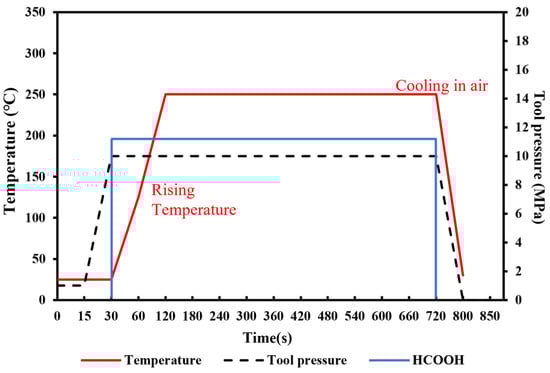
Figure 4.
Schematic diagram of original bonding parameters with gradient temperature of 150 °C/250 °C under the pressure of 10 MPa.
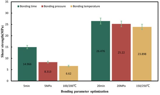
Figure 5.
Shear strength summary for all the bonding parameters in the gradient bonding.
3.2. IMC Comparison of Thermal Gradient Bonding and Isothermal Bonding
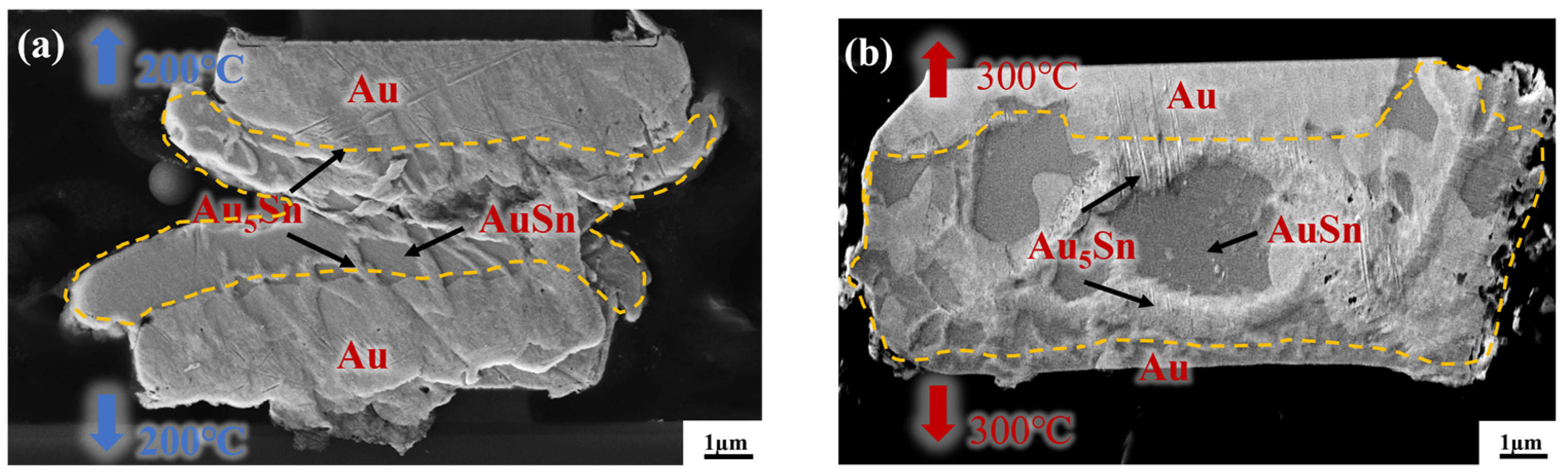
To reveal the underlying reason for the high strength of the gradient bonding, IMC comparison was first conducted between the isothermal bonding and thermal gradient bonding. Figure 6a,b depict the cross-sectional morphology of Au-Sn/Sn-Au bumps after the isothermal bonding at uniform temperatures of 200 °C and 300 °C for 10 min, respectively. Figure 6a demonstrates there is a small amount of Au5Sn and Au-Sn phases at the interface based on the energy-dispersive spectroscopy. However, a substantial quantity of metallic Sn remained unconsumed for the IMC formation. This illustrates that the IMC, at the temperature of 200 °C for 10 min, forms quite slowly and the temperature alone is insufficient for inducing high growth rates. Then, the isothermal bonding temperature rose to 300 °C to increase the IMC growth rate. Figure 6b presents the cross-sectional morphology of IMC at the bonding temperature of 300 °C for 10 min. It is evident that most of the metallic Sn within the bonding area was almost consumed within 10 min, resulting in the formation of two phases: Au5Sn and Au-Sn. The rationale behind this observation is that the bonding temperature of 300 °C surpasses the melting point of metallic Sn. Consequently, Sn exists in a molten state during the bonding process, facilitating diffusion. However, Sn overflow will happen and leads to larger bonding interface size. Additionally, high temperatures may pose the risk of device damage.
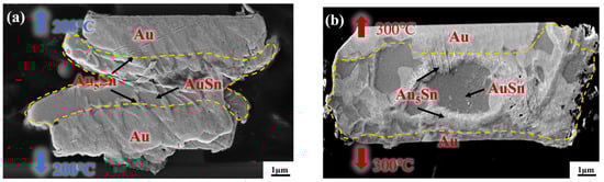
Figure 6.
Cross-section observation of the bump IMC at the bonding temperature of (a) 200 °C and (b) 300 °C.
Figure 7 presents a cross-sectional view of Au/Sn-Sn/Au bumps at the thermal gradient bonding (TGB) with the temperature of 250 °C at the top heating block and 150 °C at the bottom heating block for 10 min. It shows the IMC thickness was larger than that at the isothermal temperature of 200 °C and resulted in more Au5Sn and Au-Sn phases in the IMC region. This means the bonding process consumed a significant portion of metallic Sn. This particular configuration also proves that the high bonding strength (23.898 MPa in Figure 5) comes from the thick IMC for TGB bonding with a temperature gradient of 150 and 250 °C. The high strength can satisfy the subsequent chip stacking, credited to the abundant Au5Sn and Au-Sn grains.
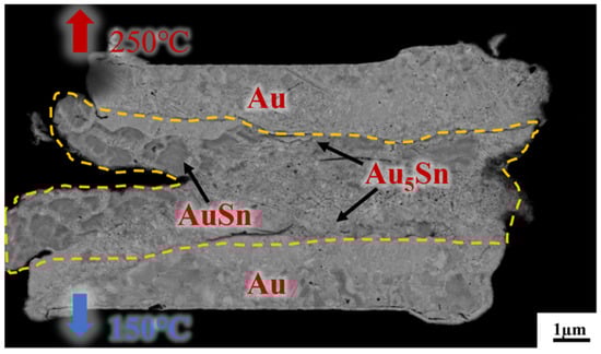
Figure 7.
Cross-section observation of the bump IMC at the bonding temperature of 150 °C/250 °C, with a bonding pressure of 10 MPa and bonding time of 10 min.
3.3. Temperature Distribution Simulation during Bonding
In conventional bonding processes, identical temperatures are applied at the upper and bottom ends of a chip using a heating block. Heat spreads from both ends toward the center, which is referred to as isothermal bonding. After a certain period, a steady state is attained. Temperature gradient bonding (TGB) involves applying different temperatures at the two ends of bonded chips. To evaluate whether a temperature gradient exists in the TGB bonding process in our study, finite element simulation was conducted. The aim was to ascertain whether the temperature in the bonding surface remains below the melting point of Sn after reaching the steady state. Through this, we can determinate whether the Au-Sn diffusion process experiences solid-state diffusion or liquid-state diffusion.
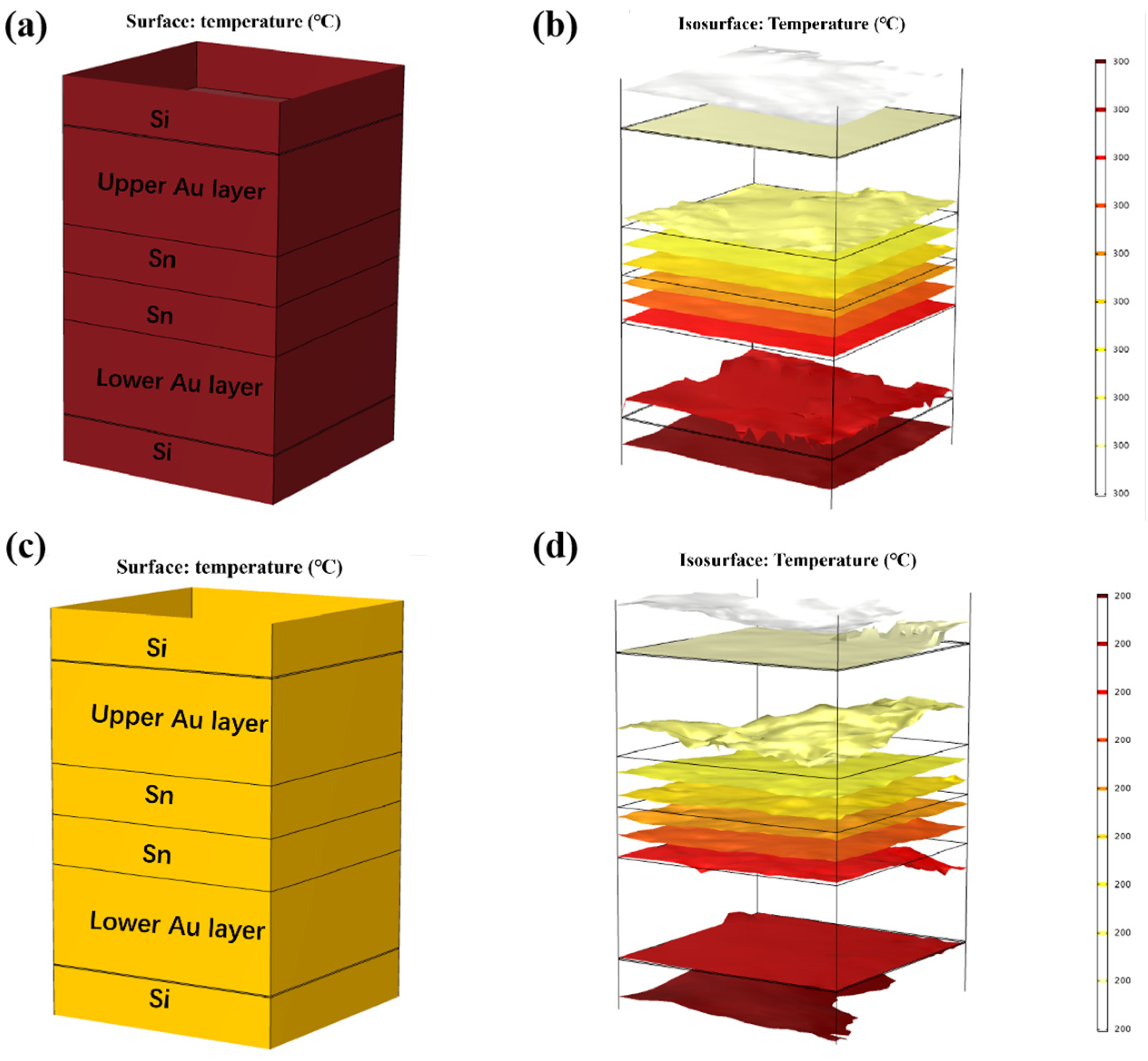
Thermal diffusion simulations of isothermal bonding and TGB bonding were all conducted. The material parameters are shown in Table 1. First, isothermal bonding simulation was designed, as below. Considering that the Au-Sn bonding temperature typically exceeds 280 °C, the temperatures of the top and bottom heating blocks were set to 300 °C and 200 °C, as shown in Figure 8. The ambient temperature was set to 25 °C. The results, depicted in Figure 8a–d, revealed that the temperature within the Au/Sn bumps reached the thermal equilibrium after 10 min, yielding overall temperatures of 300 °C and 200 °C, respectively.

Table 1.
Thermomechanical parameters of the simulated materials.

Figure 8.
Thermal diffusion simulation of isothermal bonding at 300 °C: (a) temperature distribution diagram; (b) isotherm distribution diagram. Thermal diffusion simulation of isothermal bonding at 200 °C: (c) temperature distribution diagram; (d) isotherm distribution diagram.
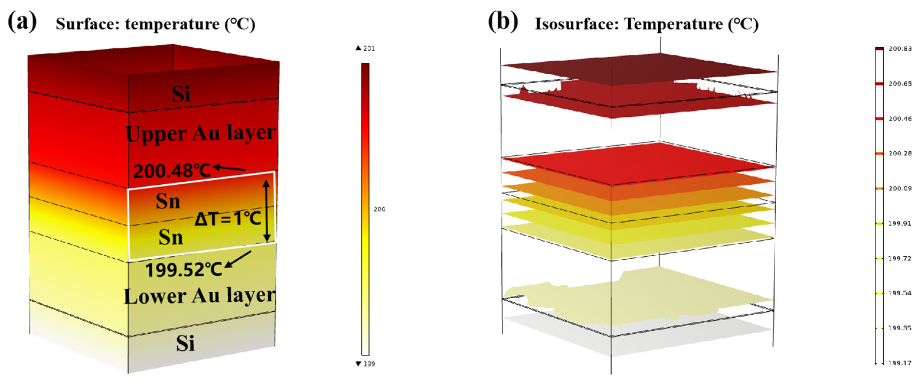
Finite element simulation was carried out on the temperature gradient bonding (TGB). The top heating block was maintained at 250 °C, the bottom heating block was set at 150 °C, and the ambient temperature was set at 25 °C. As demonstrated in Figure 9a,b, thermal equilibrium was achieved within 0.01 s of heating initiation. This is attributed to the high thermal conductivity of Si, and the thin bonding metalayer totaling less than 13 µm. It also showed that the temperature within the Sn bump was around 200 °C, which was lower than the melting point of Sn. This finding confirms that the Au-Sn diffusion in the bonding process referred to the solid-state diffusion process. Moreover, the temperature gradient at the two ends of Sn layer was 1 °C. Divided by the Sn layer thickness of 4 µm, the temperature gradient was 2500 °C/cm. Existing studies suggest that the temperature gradient of 400 °C/cm is adequate to drive the atomic diffusion of Cu atoms through metal Sn [22]. An Au atom size (134) was a little larger than Cu (117) with the same lattice structure. Thus, the threshold to drive the atomic diffusion of Au atoms through metal Sn would be a little larger than that for Cu. In our study, the temperature gradient of 2500 °C/cm significantly surpassed the threshold, and thus it can drive Au atom diffusion through metal Sn. So the low-temperature Au-Sn bonding by TGB was confirmed due to the solid-state diffusion driven by the high temperature gradient in this study.

Figure 9.
Finite element simulation of TGB thermal diffusion: (a) temperature distribution diagram; (b) isotherm distribution diagram.
3.4. Au-Sn Bonding Interface under High-Temperature Annealing
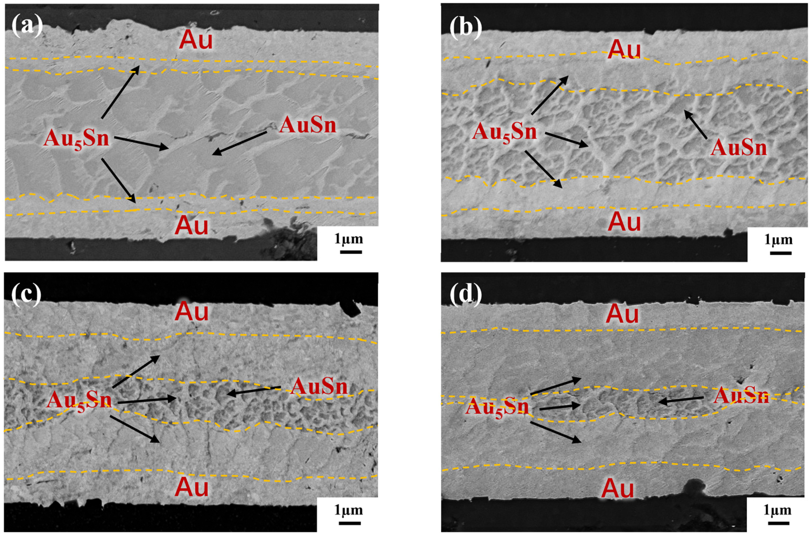
To reveal the IMC evolution, the annealing test was carried out on the blanket Au-Sn-Au without a bump in the gradient bonding. Figure 10 separately illustrates the cross-section observation of the as-bonded samples and samples subjected to varying annealing times. In Figure 10a, it was revealed that two phases, Au5Sn and Au-Sn, are formed for as-bonded samples. The Au5Sn phase evenly distributes in the upper and lower interconnections within the reaction zone. The IMC morphology takes a like-dendritic form. The Au-Sn phase is enveloped by the Au5Sn phase. Figure 10b illustrates the bonding interface after 30 min annealing. At this stage, Sn is completely depleted and transformed into two phases: Au5Sn and Au-Sn. It is noticeable that Au-Sn starts to decrease in size with there is an increase in surrounding Au5Sn. The reason for this is due to the fact that long-time annealing causes more Au to react with Au-Sn, and more Au5Sn occurs. The continuous emergence of Au5Sn comes at the expense of Au and Au-Sn consumption [13], progressively reducing the Au-Sn grains. Simultaneously, the IMC thickness in the center with Au-Sn surrounded by Au5Sn becomes smaller. Figure 10c further convinces this assumption. After 60 min annealing, the Au-Sn size continues shrinking. The IMC interface including both Au-Sn and Au5Sn becomes smaller, which is hard to discern. Only a more pronounced IMC interface with a thickness of approximately 1 µm in the center was found. After 120 min of annealing treatment, as shown in Figure 10d, the conspicuous IMC interface almost disappears, leaving a large area of Au5Sn and Au.
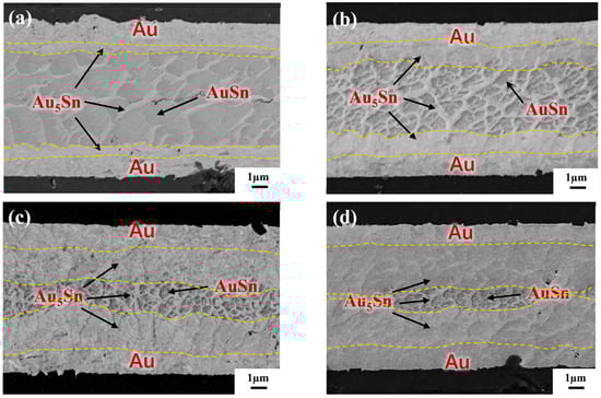
Figure 10.
IMC evolution by TGB under different annealing times: (a) as-bonded (at the bonding temperature of 150 °C–250 °C with a bonding pressure of 10 MPa and bonding time of 10 min); (b) annealing for 30 min; (c) annealing for 60 min; and (d) annealing for 120 min.
4. Conclusions
Based on the findings and insights garnered in this study, the following conclusions and design guidelines can be drawn:
- (1)
- The systematic optimization of Au-Sn bonding parameters, encompassing the bonding temperature, bonding time, and bonding pressure, leads to an optimized shear strength of 23.898 MPa. The corresponding bonding parameters contains gradient temperatures of 150 °C/250 °C and a bonding pressure of 10 MPa for 10 min in a HCOOH environment. IMC observation proves the high bonding strength comes from the thick IMC.
- (2)
- Finite element simulations validated that the Au-Sn TGB bonding was solid-state bonding. It confirms when the bonding temperatures of 150 °C at the bottom and 250 °C at the top was set, the centered bonding region had the temperature around 200 °C. This resulted in a temperature gradient of 2500 °C/cm, significantly exceeding the threshold required for driving Au atoms through metal Sn. Thus, it facilitated low-temperature solid-state Au-Sn bonding.
- (3)
- IMC evolution was explored by changing the annealing time after bonding under the optimized bonding condition. It reveals that the prolonged annealing duration results in the progressive formation of Au5Sn. Once Sn is depleted, Au-Sn and Au atoms combine to generate Au5Sn.
Author Contributions
W.W.: Conceptualization, investigation, experimentation, simulation, writing—original draft. Z.L.: supervision, conceptualization, review and editing. D.Q.: supervision, conceptualization. Z.Z.: supervision, conceptualization. N.Y.: supervision, conceptualization. S.D.: supervision, conceptualization. D.W.Z.: supervision, conceptualization. All authors have read and agreed to the published version of the manuscript.
Funding
This work was supported by STI 2030-Major Projects (2022ZD0209200), and the project of MOE Innovation Platform. The paper is also supported by Open Research Fund of China National Key Laboratory of Materials for Integrated Circuits (NKLJC-K2023-12) and National Natural Science Foundation of China (62074132).
Data Availability Statement
Data are contained within the article.
Conflicts of Interest
The authors declare no conflict of interest.
References
- Suk, K.L.; Choo, K.; Kim, S.J.; Kim, J.S.; Paik, K.W. Studies on various chip-on-film (COF) packages using ultra fine pitch two-metal layer flexible printed circuits (two-metal layer FPCs). Microelectron. Reliab. 2012, 52, 1182–1188. [Google Scholar] [CrossRef]
- Szostak, K.M.; Keshavarz, M.; Constandinou, T.G. Hermetic chip-scale packaging using Au: Sn eutectic bonding for implantable devices. J. Micromech. Microeng. 2021, 31, 095003. [Google Scholar] [CrossRef]
- Lim, S.P.S.; Rao, V.S.; Hnin, W.Y.; Ching, W.L.; Kripesh, V.; Lee, C.; Lau, J.; Milla, J.; Fenner, A. Process development and reliability of microbumps. IEEE Trans. Compon. Packag. Technol. 2010, 33, 747–753. [Google Scholar] [CrossRef]
- Lee, Y.K.; Ko, Y.H.; Kim, J.K.; Lee, C.W.; Yoo, S. The effect of intermetallic compound evolution on the fracture behavior of Au stud bumps joined with Sn-3.5 Ag solder. Electron. Mater. Lett. 2013, 9, 31–39. [Google Scholar] [CrossRef]
- Ko, C.T.; Hsiao, Z.C.; Chang, Y.J.; Chen, P.S.; Hwang, Y.J.; Fu, H.C.; Huang, J.H.; Chiang, C.W.; Sheu, S.S.; Chen, Y.H.; et al. A wafer-level three-dimensional integration scheme with Cu TSVs based on microbump/adhesive hybrid bonding for three-dimensional memory application. IEEE Trans. Device Mater. Reliab. 2012, 12, 209–216. [Google Scholar] [CrossRef]
- Arabi, F.; Theolier, L.; Martineau, D.; Deletage, J.-Y.; Medina, M.; Woirgard, E. Power electronic assemblies: Thermo-mechanical degradations of gold-tin solder for attaching devices. Microelectron. Reliab. 2016, 64, 409–414. [Google Scholar] [CrossRef]
- Zeng, G.; McDonald, S.; Nogita, K. Development of high-temperature solders. Microelectron. Reliab. 2012, 52, 1306–1322. [Google Scholar] [CrossRef]
- Xu, H.; Suni, T.; Vuorinen, V.; Li, J.; Heikkinen, H.; Monnoyer, P.; Paulasto-Kröckel, M. Wafer-level SLID bonding for MEMS encapsulation. Adv. Manuf. 2013, 1, 226–235. [Google Scholar] [CrossRef]
- Rautiainen, A.; Vuorinen, V.; Heikkinen, H.; Paulasto-Krockel, M. Wafer-level Au-Sn/Pt solid–liquid interdiffusion bonding. IEEE Trans. Compon. Packag. Manuf. Technol. 2018, 8, 169–176. [Google Scholar] [CrossRef]
- Sood, S.; Hergert, R.; Treichel, O. Metal Inter-Diffusion and Eutectic Wafer Bonding Processes for Advanced Mems Packaging. In Proceedings of the IWLPC (Wafer-Level Packaging) Conference, San Jose, CA, USA, 6–7 November 2013. [Google Scholar]
- Li, D.; Shang, Z.; She, Y.; Wen, Z. Investigation of Au/Si eutectic wafer bonding for MEMS accelerometers. Micromachines 2017, 8, 158. [Google Scholar] [CrossRef]
- Chu, K.; Park, S.; Lee, C.; Sohn, Y. Effect of multiple flip-chip assembly on the mechanical reliability of eutectic Au–Sn solder joint. J. Mater. Sci. Mater. Electron. 2016, 27, 9941–9946. [Google Scholar] [CrossRef]
- Garnier, A.; Baillin, X.; Hodaj, F. Solidification and interfacial interactions in gold–tin system during eutectic or thermo-compression bonding for 200 mm MEMS wafer level hermetic packaging. J. Mater. Sci. Mater. Electron. 2013, 24, 5000–5013. [Google Scholar] [CrossRef]
- Tez, S.; Torunbalci, M.M.; Akin, T. A novel method for fabricating MEMS three-axis accelerometers using low temperature Au-Sn eutectic bonding. In Proceedings of the 2016 IEEE SENSORS, Orlando, FL, USA, 30 October–3 November 2016; pp. 1–3. [Google Scholar]
- Temel, O.; Kalay, Y.E.; Akin, T. Wafer-Level Low-Temperature Solid-Liquid Inter-Diffusion Bonding with Thin Au-Sn Layers for MEMS Encapsulation. J. Microelectromech. Syst. 2020, 30, 64–71. [Google Scholar] [CrossRef]
- Kim, S.K.; Oh, T.S. Microstructure and Contact Resistance of the Au-Sn Flip-Chip Joints Processed by Electrodeposition. J. Microelectron. Packag. Soc. 2008, 15, 9–15. [Google Scholar]
- Duan, A.; Luu, T.-T.; Wang, K.; Aasmundtveit, K.; Hoivik, N. Wafer-level Cu–Sn micro-joints with high mechanical strength and low Sn overflow. J. Micromech. Microeng. 2015, 25, 097001. [Google Scholar] [CrossRef]
- Fang, Z.; Mao, X.; Yang, J.; Yang, F. A wafer-level Sn-rich Au–Sn intermediate bonding technique with high strength. J. Micromech. Microeng. 2013, 23, 095008. [Google Scholar] [CrossRef]
- Zhu, Z.X.; Li, C.C.; Liao, L.L.; Liu, C.K.; Kao, C.R. Au–Sn bonding material for the assembly of power integrated circuit module. J. Alloys Compd. 2016, 671, 340–345. [Google Scholar] [CrossRef]
- Yang, C.Y.; Laksono, A.D.; Yen, Y.W.; Guo, Y.Z.; Wang, C.H.; Li, J.L.; Chiang, T.Y. Investigation of phase equilibria of the Au–Ni–Sn ternary system and interfacial reactions in the Au/Sn/Ni/Cu multilayer couple. Mater. Chem. Phys. 2022, 289, 126494. [Google Scholar] [CrossRef]
- Wang, Y.-H.; Nishida, K.; Hutter, M.; Kimura, T.; Suga, T. Low-temperature process of fine-pitch Au–Sn bump bonding in ambient air. Jpn. J. Appl. Phys. 2007, 46, 1961. [Google Scholar] [CrossRef]
- Yang, T.L.; Aoki, T.; Matsumoto, K.; Toriyama, K.; Horibe, A.; Mori, H.; Orii, Y.; Wu, J.Y.; Kao, C.R. Full intermetallic joints for chip stacking by using thermal gradient bonding. Acta Mater. 2016, 113, 90–97. [Google Scholar] [CrossRef]
- Liu, X.; He, S.; Nishikawa, H. Low temperature solid-state bonding using Sn-coated Cu particles for high temperature die attach. J. Alloys Compd. 2017, 695, 2165–2172. [Google Scholar] [CrossRef]
- Wang, W.; Liu, Z.; Zhu, Z.; Chen, L.; Sun, Q. Low Temperature Au/Sn Solid-Liquid Diffusion Chip-to-Chip Bonding for MEMS Encapsulation. In Proceedings of the 2022 23rd International Conference on Electronic Packaging Technology (ICEPT), Dalian, China, 10–13 August 2022; pp. 1–5. [Google Scholar]
- Wang, J.; Wang, Q.; Wu, Z.; Wang, D.; Cai, J. Solid-state-diffusion bonding for wafer-level fine-pitch Cu/Sn/Cu interconnect in 3-D integration. IEEE Trans. Compon. Packag. Manuf. Technol. 2016, 7, 19–26. [Google Scholar] [CrossRef]
- Shi, H.; Che, F.; Tian, C.; Zhang, R.; Park, J.T.; Ueda, T. Analysis of edge and corner bonded PSvfBGA reliability under thermal cycling conditions by experimental and finite element methods. Microelectron. Reliab. 2012, 52, 1870–1875. [Google Scholar] [CrossRef]
- Chen, M.; Zhang, Y.; Guo, Y.; Wu, T.; Dou, L.; Tian, W.; Xiao, J.; Li, J. Research on Flip-Chip Bonding Process and Thermal Cycle Reliability Simulation of 3-D Stacked Structure. IEEE Trans. Compon. Packag. Manuf. Technol. 2021, 12, 51–58. [Google Scholar] [CrossRef]
- Lu, T.; Jin, J.M. Coupled electrical–thermal–mechanical simulation for the reliability analysis of large-scale 3-D interconnects. IEEE Trans. Compon. Packag. Manuf. Technol. 2017, 7, 229–237. [Google Scholar] [CrossRef]
- Huang, C.; Tang, W.; Zhang, L. The bonding forming simulation and reliability research of the flip-chip stacked gold stud bump. IEEE Trans. Compon. Packag. Manuf. Technol. 2016, 7, 153–161. [Google Scholar] [CrossRef]
- Zhu, J.; Zhang, J.; Loula, A.F.D.; Bevilacqua, L. Mixed variational formulation and numerical analysis of thermally coupled nonlinear Darcy flows. SIAM J. Numer. Anal. 2013, 51, 2746–2772. [Google Scholar] [CrossRef]
- Cannarozzi, A.A.; Momanyi, F.X.; Ubertini, F. A hybrid flux model for heat conduction problems. Int. J. Numer. Methods Eng. 2000, 47, 1731–1749. [Google Scholar] [CrossRef]


Disclaimer/Publisher’s Note: The statements, opinions and data contained in all publications are solely those of the individual author(s) and contributor(s) and not of MDPI and/or the editor(s). MDPI and/or the editor(s) disclaim responsibility for any injury to people or property resulting from any ideas, methods, instructions or products referred to in the content. |
© 2023 by the authors. Licensee MDPI, Basel, Switzerland. This article is an open access article distributed under the terms and conditions of the Creative Commons Attribution (CC BY) license (https://creativecommons.org/licenses/by/4.0/).