
A Low-Power SAR ADC with Capacitor-Splitting Energy-Efficient Switching Scheme for Wearable Biosensor Applications

 , , , ,
Abstract
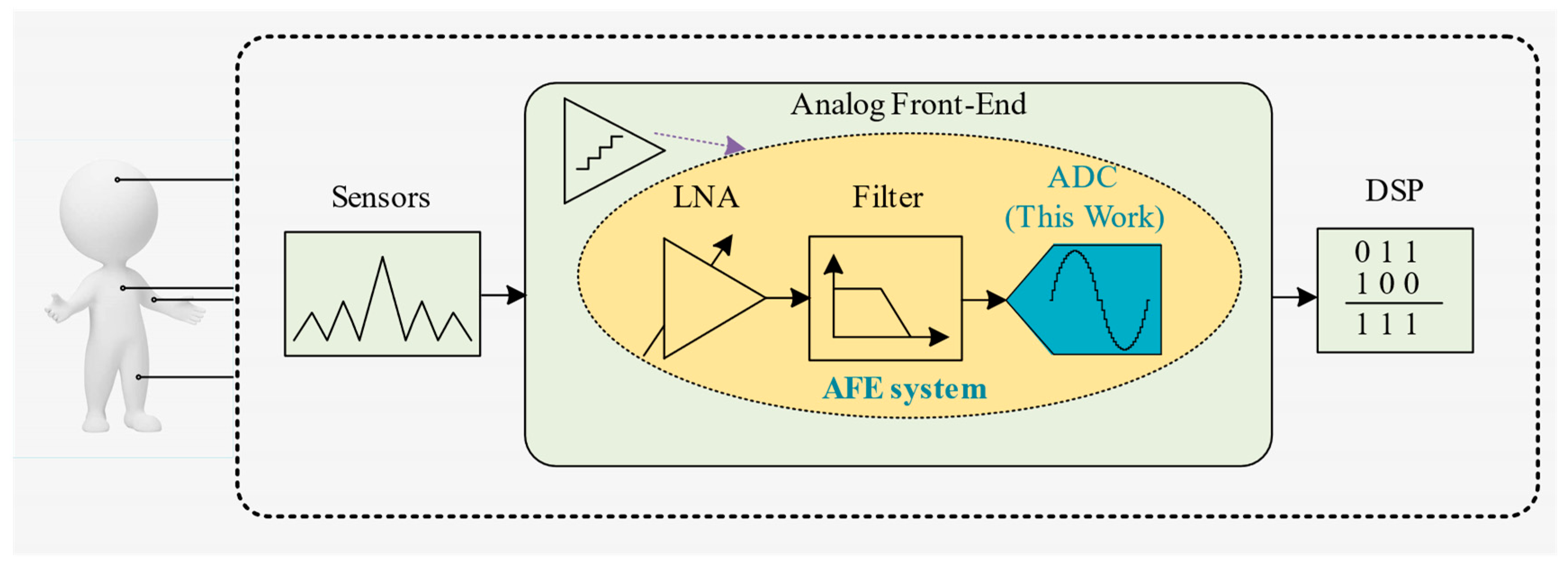
:1. Introduction

| Type of Biological Signals | Frequency Range (Hz) | Amplitude (mV) |
|---|---|---|
| ECG | 0.01 to 250 | 0.5 to 4 |
| EMG | Up to 2 K | 0.1 to 5 |
| EEG | 0.5 to 150 | 0.0005 to 0.3 |
| ECoG | 70 to 110 | 0.001 to 3 |
2. Design of the Proposed SAR ADC
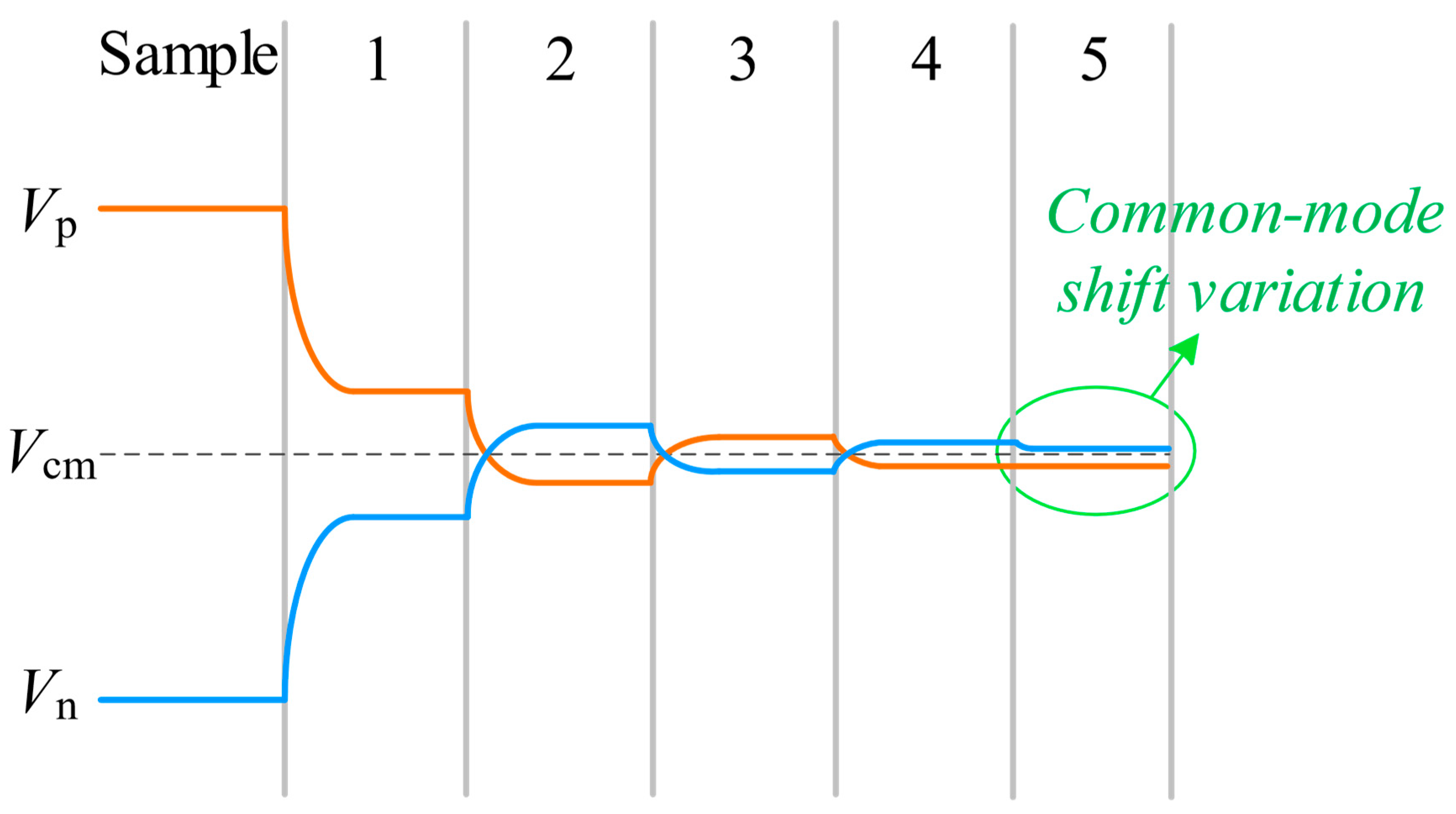
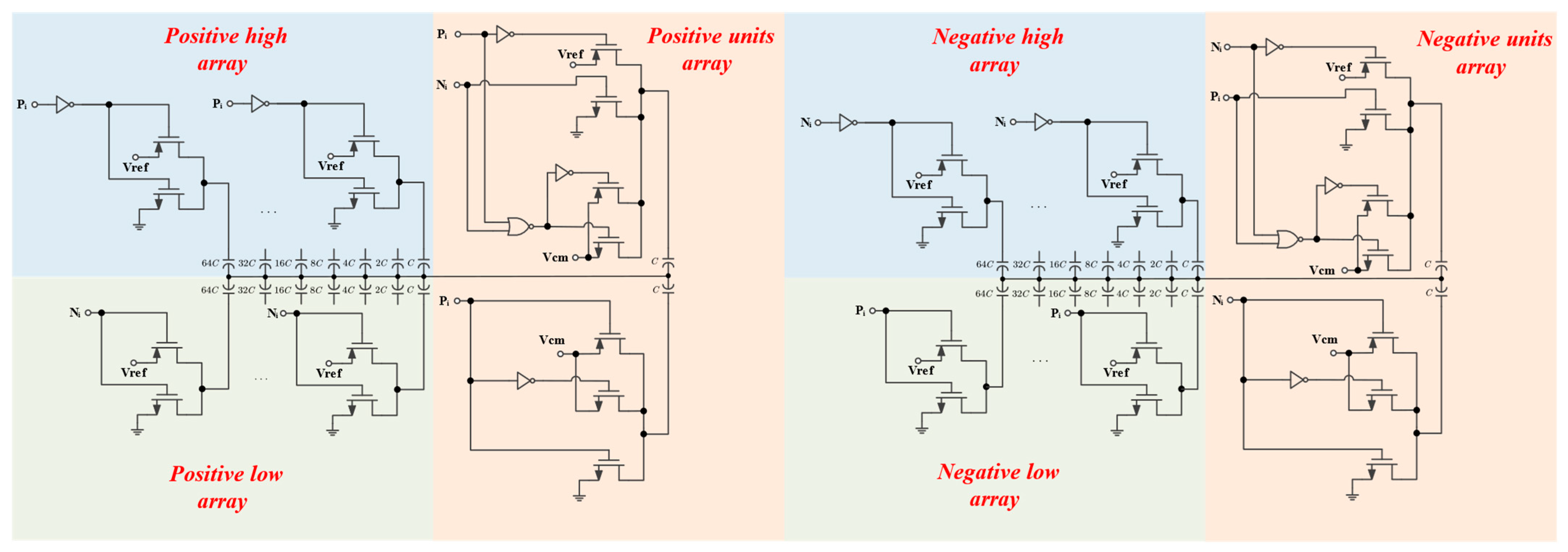
2.1. DAC Switching Scheme
2.2. Bootstrapped Sampling Switch
2.3. Dynamic Comparator
2.4. Dynamic SAR Logic
2.5. DAC Driver Circuit Design
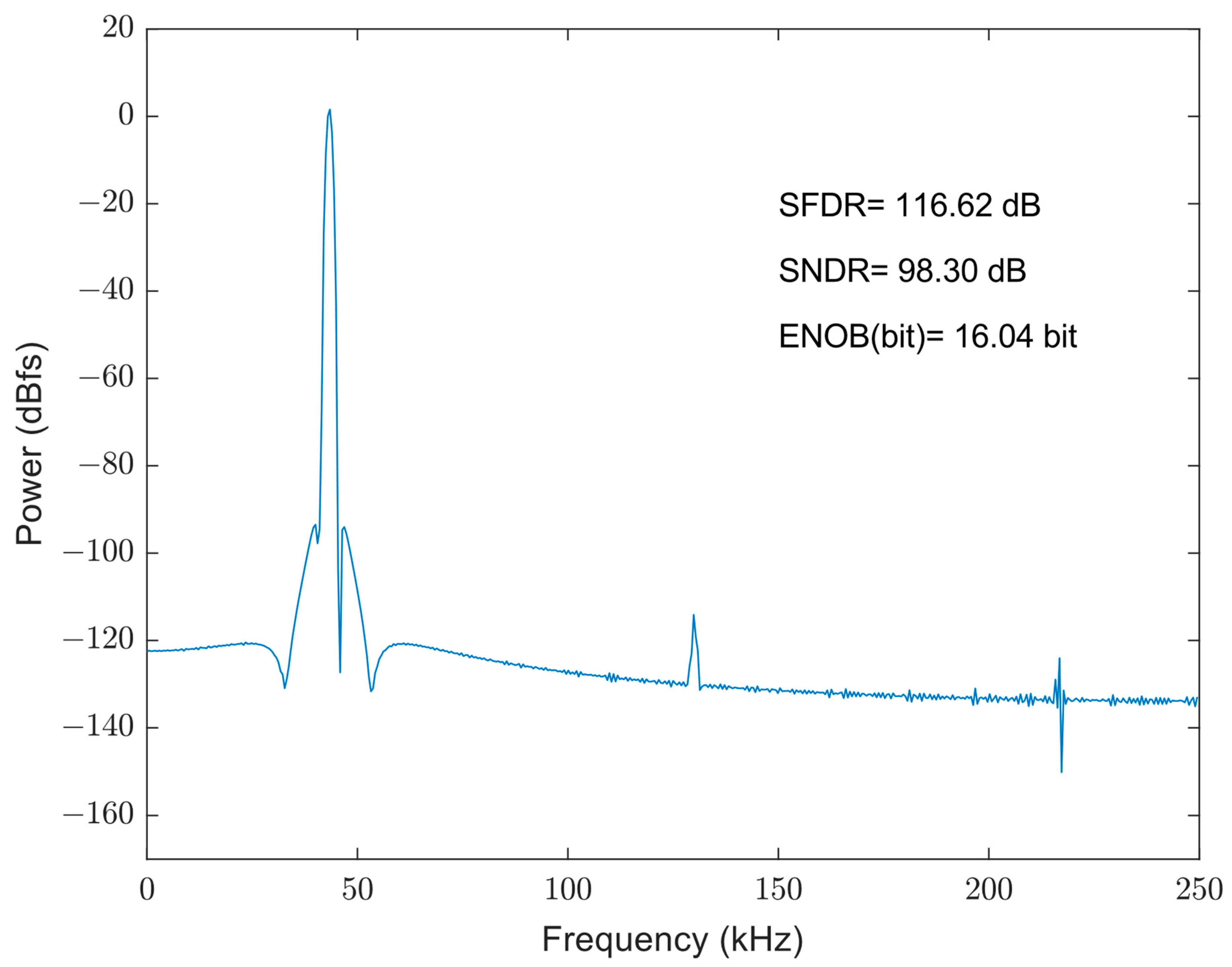
3. Analysis of Results
4. Conclusions
Author Contributions
Funding
Data Availability Statement
Conflicts of Interest
References
- Tai, H.-Y.; Hu, Y.-S.; Chen, H.-W.; Chen, H.-S. 11.2 A 0.85fJ/Conversion-Step 10b 200kS/s Subranging SAR ADC in 40nm CMOS. In Proceedings of the 2014 IEEE International Solid-State Circuits Conference Digest of Technical Papers (ISSCC), San Francisco, CA, USA, 9–13 February 2014; pp. 196–197. [Google Scholar]
- Kim, H.; Kim, S.; Van Helleputte, N.; Artes, A.; Konijnenburg, M.; Huisken, J.; Van Hoof, C.; Yazicioglu, R.F. A Configurable and Low-Power Mixed Signal SoC for Portable ECG Monitoring Applications. IEEE Trans. Biomed. Circuits Syst. 2014, 8, 257–267. [Google Scholar] [CrossRef]
- Zhao, X.; Li, D.; Zhang, X.; Liu, S.; Zhu, Z. A 0.6-V 94-nW 10-Bit 200-kS/s Single-Ended SAR ADC for Implantable Biosensor Applications. IEEE Sens. J. 2022, 22, 17904–17913. [Google Scholar] [CrossRef]
- Yuan, C.; Ng, K.A.; Xu, Y.P.; Yen, S.-C.; Thakor, N.V. A 1-V 9.8-ENOB 100-kS/s Single-Ended SAR ADC with Symmetrical DAC Switching Technique for Neural Signal Acquisition. In Proceedings of the 2015 IEEE Asian Solid-State Circuits Conference (A-SSCC), Xia’men, China, 9–11 November 2015; pp. 1–4. [Google Scholar]
- Aneesh, K.; Manoj, G.; Shylu Sam, S. Design Approaches of Ultra-Low Power SAR ADC for Biomedical Systems—A Review. J. Circuit Syst. Comput. 2022, 31, 2230009. [Google Scholar] [CrossRef]
- Tyagi, M.; Mittal, P.; Kumar, P. Design of 8 -Bit Low Power SAR ADC in 45 Nm for Biomedical Implants. Phys. Scr. 2023, 98, 116101. [Google Scholar] [CrossRef]
- Tong, X.; Ghovanloo, M. Energy-efficient Switching Scheme in SAR ADC for Biomedical Electronics. Electron. Lett. 2015, 51, 676–678. [Google Scholar] [CrossRef]
- McCreary, J.L.; Gray, P.R. All-MOS Charge Redistribution Analog-to-Digital Conversion Techniques. I. IEEE J. Solid-State Circuits 1975, 10, 371–379. [Google Scholar] [CrossRef]
- Liu, C.-C.; Chang, S.-J.; Huang, G.-Y.; Lin, Y.-Z. A 10-Bit 50-MS/s SAR ADC With a Monotonic Capacitor Switching Procedure. IEEE J. Solid-State Circuits 2010, 45, 731–740. [Google Scholar] [CrossRef]
- Zhu, Y.; Chan, C.-H.; Chio, U.-F.; Sin, S.-W.; Seng-Pan, U.; Martins, R.P.; Maloberti, F. A 10-Bit 100-MS/s Reference-Free SAR ADC in 90 Nm CMOS. IEEE J. Solid-State Circuits 2010, 45, 1111–1121. [Google Scholar] [CrossRef]
- Wang, H.; Zhu, Z. Energy-Efficient and Reference-Free Monotonic Capacitor Switching Scheme with Fewest Switches for SAR ADC. IEICE Electron. Express 2015, 12, 20141202. [Google Scholar] [CrossRef]
- Zhang, H.; Zhang, H.; Zhang, R. Energy-efficient Higher-side-reset-and-set Switching Scheme for SAR ADC. Electron. Lett. 2017, 53, 1238–1240. [Google Scholar] [CrossRef]
- Hsieh, S.-E.; Hsieh, C.-C. A 0.3-V 0.705-fJ/Conversion-Step 10-Bit SAR ADC with a Shifted Monotonic Switching Procedure in 90-Nm CMOS. IEEE Trans. Circuits Syst. II 2016, 63, 1171–1175. [Google Scholar] [CrossRef]
- Hu, Y.; Yi, Z.; He, Z.; Li, B. Energy-Efficient, Area-Efficient, High-Accuracy and Low-Complexity Switching Scheme for SAR ADC. IEICE Electron. Express 2017, 14, 20170428. [Google Scholar] [CrossRef]
- Yang, C.; Olieman, E.; Litjes, A.; Qiu, L.; Tang, K.; Zheng, Y.; Van Veldhoven, R. An Area-Efficient SAR ADC With Mismatch Error Shaping Technique Achieving 102-dB SFDR 90.2-dB SNDR Over 20-kHz Bandwidth. IEEE Trans. VLSI Syst. 2021, 29, 1575–1585. [Google Scholar] [CrossRef]
- Zhang, H.; Zhang, H.; Sun, Q.; Li, J.; Liu, X.; Zhang, R. A 0.6-V 10-Bit 200-kS/s SAR ADC With Higher Side-Reset-and-Set Switching Scheme and Hybrid CAP-MOS DAC. IEEE Trans. Circuits Syst. I 2018, 65, 3639–3650. [Google Scholar] [CrossRef]
- Jian, M.; Zheng, J.; Kong, X.; Yuan, M.; Zhang, C.; Guo, C.; Sun, B. A 12-Bit SAR ADC with a Reversible VCM-Based Capacitor Switching Scheme. Microelectron. J. 2022, 129, 105588. [Google Scholar] [CrossRef]
- Tong, X.; Zhao, S.; Xin, X. High Energy Efficiency and Linearity Switching Scheme Without Reset Energy for SAR ADC. Circuits Syst. Signal Process. 2022, 41, 5872–5894. [Google Scholar] [CrossRef]
- Huang, L.; Li, J.; Jiang, X.; Wu, J. A 2.1-fJ/Conversion-Step 10-Bit 125-KS/s SAR ADC with Vcm-Based Bidirectional Single-Side Switching Scheme. In Proceedings of the 2023 12th International Conference on Modern Circuits and Systems Technologies (MOCAST), Athens, Greece, 28–30 June 2023; pp. 1–4. [Google Scholar]
- Wu, Y.; Cheng, X.; Zeng, X. A 960 μW 10-Bit 70-MS/s SAR ADC with an Energy-Efficient Capacitor-Switching Scheme. Microelectron. J. 2013, 44, 1260–1267. [Google Scholar] [CrossRef]
- Mekkattillam, Y.; Mohapatra, S.; Mohapatra, N.R. Design and Calibration of 14-Bit 10 KS/s Low Power SAR ADC for Bio-Medical Applications. In VLSI Design and Test; Sengupta, A., Dasgupta, S., Singh, V., Sharma, R., Kumar Vishvakarma, S., Eds.; Communications in Computer and Information Science; Springer Singapore: Singapore, 2019; Volume 1066, pp. 590–604. ISBN 978-981-329-766-1. [Google Scholar]
- Mandrumaka, K.K.; Noorbasha, F. A Low Power 10 Bit SAR ADC with Variable Threshold Technique for Biomedical Applications. SN Appl. Sci. 2019, 1, 918. [Google Scholar] [CrossRef]
- Lin, J.-Y.; Hsieh, C.-C. A 0.3 V 10-Bit 1.17 f SAR ADC With Merge and Split Switching in 90 Nm CMOS. IEEE Trans. Circuits Syst. I 2015, 62, 70–79. [Google Scholar] [CrossRef]
- Huang, G.-Y.; Chang, S.-J.; Liu, C.-C.; Lin, Y.-Z. 10-Bit 30-MS/s SAR ADC Using a Switchback Switching Method. In IEEE Transactions on Very Large Scale Integration (VLSI) Systems; IEEE: Piscataway, NJ, USA, 2013; Volume 21, pp. 584–588. [Google Scholar] [CrossRef]
- Promitzer, G. 12 Bit Low Power Fully Differential Switched Capacitor Non-Calibrating Successive Approximation ADC with 1MS/s. In Proceedings of the 26th European Solid-State Circuits Conference, Stockholm, Sweden, 19–21 September 2000; pp. 176–179. [Google Scholar]
- Sengupta, S. Analytical Expression of HD3 Due to Non-Linear MOS Switch in MOSFET-C Sample and Hold Circuits. In Proceedings of the 2005 IEEE International Symposium on Circuits and Systems, Kobe, Japan, 23–26 May 2005; Volume 3, pp. 2251–2254. [Google Scholar]
- Lin, K.-T.; Cheng, Y.-W.; Tang, K.-T. A 0.5 V 1.28-MS/s 4.68-fJ/Conversion-Step SAR ADC With Energy-Efficient DAC and Trilevel Switching Scheme. IEEE Trans. VLSI Syst. 2016, 24, 1441–1449. [Google Scholar] [CrossRef]
- Rezapour, A.; Shamsi, H.; Abbasizadeh, H.; Lee, K.-Y. Low Power High Speed Dynamic Comparator. In Proceedings of the 2018 IEEE International Symposium on Circuits and Systems (ISCAS), Florence, Italy, 27–30 May 2018; pp. 1–5. [Google Scholar]
- Khorami, A.; Sharifkhani, M. A Low-Power High-Speed Comparator for Precise Applications. In IEEE Transactions on Very Large Scale Integration (VLSI) Systems; IEEE: Piscataway, NJ, USA, 2018; Volume 26, pp. 2038–2049. [Google Scholar] [CrossRef]
- Hussain, S.; Kumar, R.; Trivedi, G. Comparison of NMOS and PMOS Input Driving Dynamic Comparator in 45nm Technology. IOP Conf. Ser. Mater. Sci. Eng. 2021, 1020, 012022. [Google Scholar] [CrossRef]
- Doernberg, J.; Lee, H.-S.; Hodges, D.A. Full-Speed Testing of A/D Converters. IEEE J. Solid-State Circuits 1984, 19, 820–827. [Google Scholar] [CrossRef]
- Tong, X.; Song, M.; Chen, Y.; Dong, S. A 10-Bit 120 kS/s SAR ADC without Reset Energy for Biomedical Electronics. Circuits Syst. Signal Process. 2019, 38, 5411–5425. [Google Scholar] [CrossRef]
- Saisundar, S.; Cheong, J.H.; Je, M. A 1.8V 1MS/s Rail-to-Rail 10-Bit SAR ADC in 0.18 μm CMOS. In Proceedings of the 2012 IEEE International Symposium on Radio-Frequency Integration Technology (RFIT), Singapore, 21–23 November 2012; pp. 83–85. [Google Scholar]
- Verma, N.; Chandrakasan, A.P. An Ultra Low Energy 12-Bit Rate-Resolution Scalable SAR ADC for Wireless Sensor Nodes. IEEE J. Solid-State Circuits 2007, 42, 1196–1205. [Google Scholar] [CrossRef]
- Huang, H.-Y.; Lin, J.-Y.; Hsieh, C.-C.; Chang, W.-H.; Tsai, H.-H.; Chiu, C.-F. A 9.2b 47fJ/Conversion-Step Asynchronous SAR ADC with Input Range Prediction DAC Switching. In Proceedings of the 2012 IEEE International Symposium on Circuits and Systems, Seoul, Republic of Korea, 20–23 May 2012; pp. 2353–2356. [Google Scholar]
- Fu, Z.; Tang, X.; Li, D.; Wang, J.; Basak, D.; Pun, K.-P. A 10-Bit 2 MS/s SAR ADC Using Reverse VCM-Based Switching Scheme. In Proceedings of the 2016 IEEE International Symposium on Circuits and Systems (ISCAS), Montréal, QC, Canada, 22–25 May 2016; pp. 1030–1033. [Google Scholar]


| Switching Scheme | Average Energy () | Energy Saving (%) | Sensitivity to the Accuracy of Vcm | Number of References for Each Capacitor | Maximum Common-Mode Variation |
|---|---|---|---|---|---|
| Conventional [8] | 1363.3 | Reference | No | 2 | 0 LSB |
| Monotonic [9] | 255.5 | 81.26% | No | 2 | 512 LSB |
| Vcm-based [10] | 170.2 | 87.52% | Very high | 3 | 0 LSB |
| Wang et al. [11] | 128 | 90.61% | No | 2 | 512 LSB |
| HSRS [12] | 106.2 | 92.20% | Very high | 3 | 256 LSB |
| SMS [13] | 63.75 | 95.32% | Very high | 3 | 768 LSB |
| Hu et al. [14] | 63.56 | 95.34% | Very low | 2 | 256 LSB |
| Proposed | 85.08 | 93.76% | Very low (only LSB and second LSB) | 2 (all bits except second LSB) | 1 LSB |
| Parameter | [21] * | [22] * | [33] * | [34] | [35] | [36] * | This Work * |
|---|---|---|---|---|---|---|---|
| Process (nm) | 180 | 180 | 180 | 180 | 180 | 180 | 180 |
| Resolution (bits) | 14 | 10 | 10 | 12 | 10 | 10 | 10 |
| Sampling Rate (MS/s) | 0.01 | 1 | 1 | 0.1 | 0.5 | 2 | 0.2 |
| Supply Voltage (V) | 1.8 | 0.5 | 1.8 | 1 | 1 | 1.8 | 1 |
| SNDR (dB) | 84.50 | 61.96 | 58.9 | 65.3 | 57.38 | 59.59 | 61.77 |
| ENOB (bits) | 13.80 | 7.69 | 9.5 | 10.55 | 9.24 | 9.65 | 9.97 |
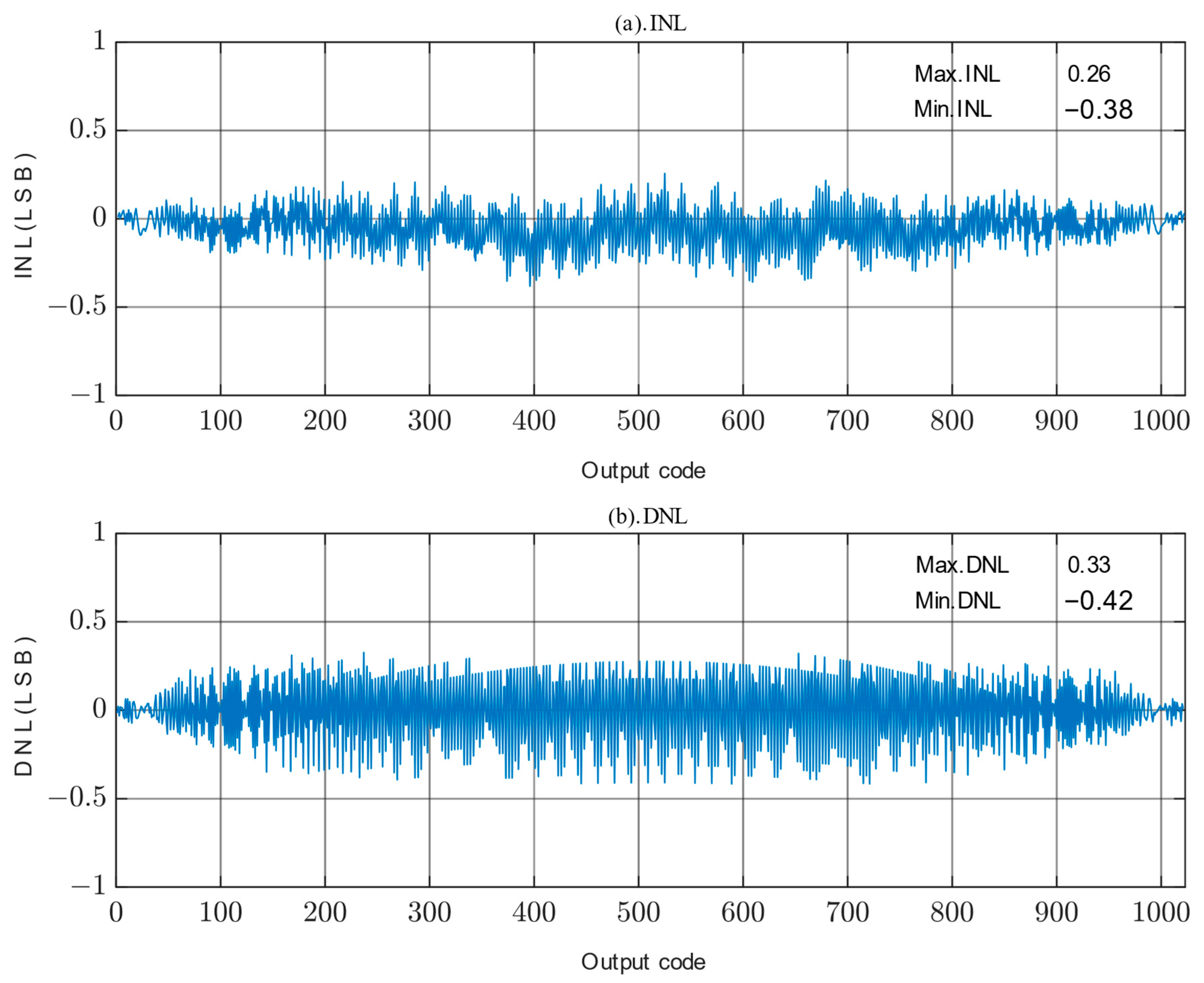
| DNL (LSB) | 0.5 | −0.82/0.9 | −0.40/0.36 | −0.19/0.19 | −0.72/0.50 | −0.23/0.23 | −0.42/0.33 |
| INL (LSB) | 0.42 | −1.31/1.06 | −0.46/0.36 | −0.16/0.16 | −0.88/0.85 | −0.23/0.23 | −0.38/0.26 |
| Power Consumption (µW) | 19.5 | 13.99 | 131 | 25 | 14.2 | 41.92 | 4.45 |
| FOM (fJ/conv. Step) | 140 | 67.7 | 181 | 165 | 47 | 26.9 | 22.2 |
Disclaimer/Publisher’s Note: The statements, opinions and data contained in all publications are solely those of the individual author(s) and contributor(s) and not of MDPI and/or the editor(s). MDPI and/or the editor(s) disclaim responsibility for any injury to people or property resulting from any ideas, methods, instructions or products referred to in the content. |
© 2023 by the authors. Licensee MDPI, Basel, Switzerland. This article is an open access article distributed under the terms and conditions of the Creative Commons Attribution (CC BY) license (https://creativecommons.org/licenses/by/4.0/).
Share and Cite
Hu, Y.; Huang, Q.; Tang, B.; Chen, C.; Hu, L.; Yu, E.; Li, B.; Wu, Z. A Low-Power SAR ADC with Capacitor-Splitting Energy-Efficient Switching Scheme for Wearable Biosensor Applications. Micromachines 2023, 14, 2244. https://doi.org/10.3390/mi14122244
Hu Y, Huang Q, Tang B, Chen C, Hu L, Yu E, Li B, Wu Z. A Low-Power SAR ADC with Capacitor-Splitting Energy-Efficient Switching Scheme for Wearable Biosensor Applications. Micromachines. 2023; 14(12):2244. https://doi.org/10.3390/mi14122244
Chicago/Turabian StyleHu, Yunfeng, Qingming Huang, Bin Tang, Chaoyi Chen, Lexing Hu, Enhao Yu, Bin Li, and Zhaohui Wu. 2023. "A Low-Power SAR ADC with Capacitor-Splitting Energy-Efficient Switching Scheme for Wearable Biosensor Applications" Micromachines 14, no. 12: 2244. https://doi.org/10.3390/mi14122244
APA StyleHu, Y., Huang, Q., Tang, B., Chen, C., Hu, L., Yu, E., Li, B., & Wu, Z. (2023). A Low-Power SAR ADC with Capacitor-Splitting Energy-Efficient Switching Scheme for Wearable Biosensor Applications. Micromachines, 14(12), 2244. https://doi.org/10.3390/mi14122244