
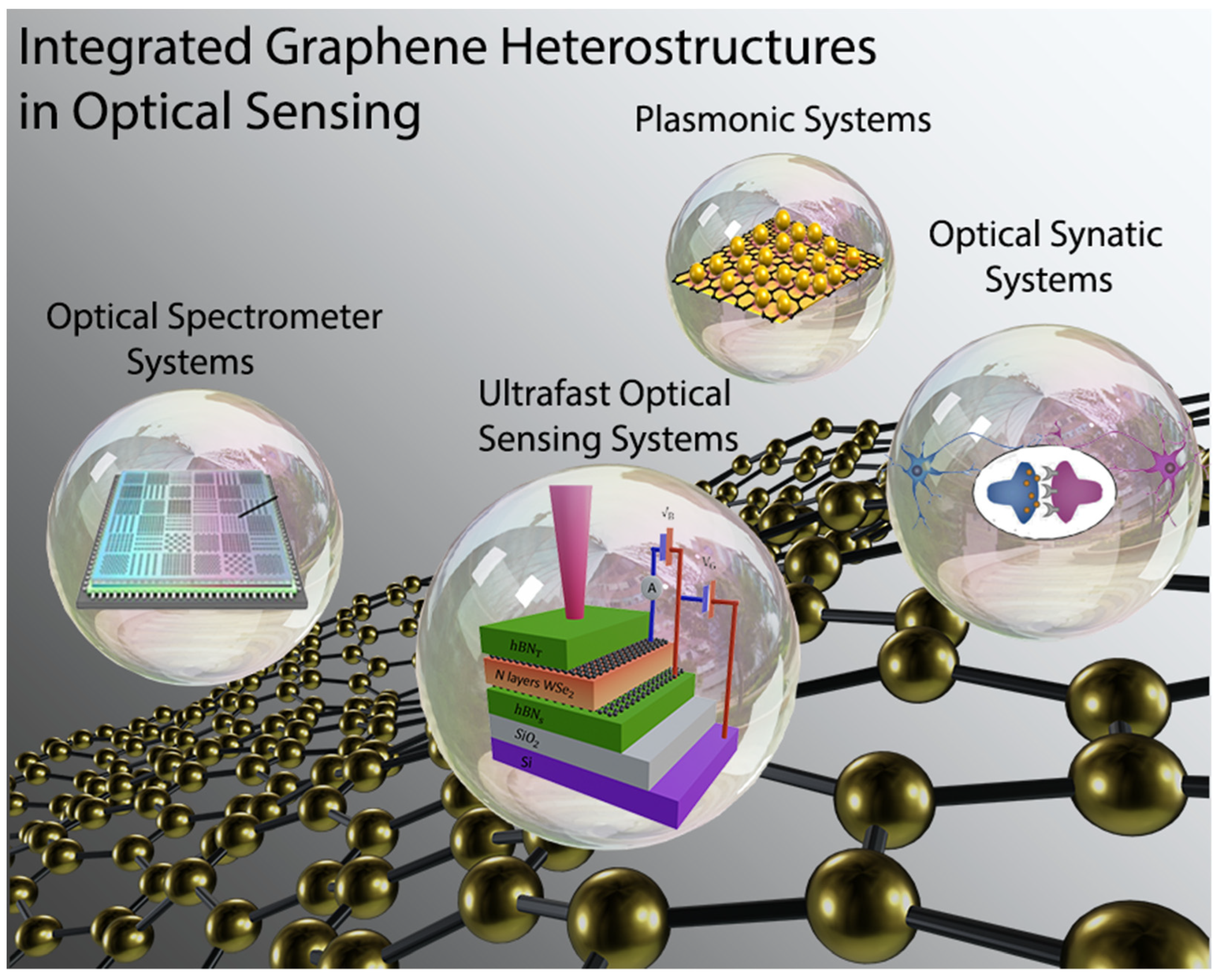
Integrated Graphene Heterostructures in Optical Sensing
 ,
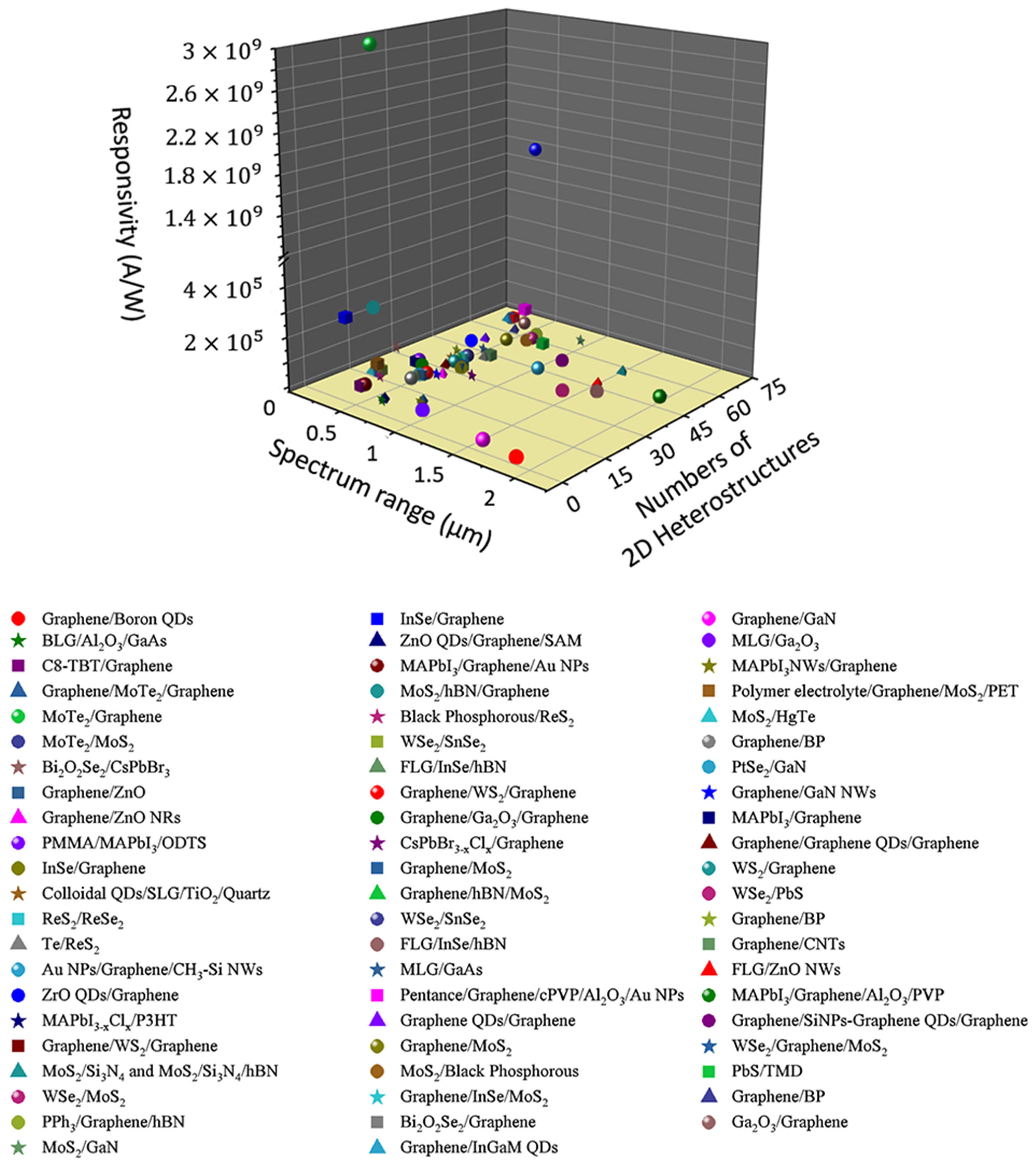
,  , , and
Abstract
:1. Introduction
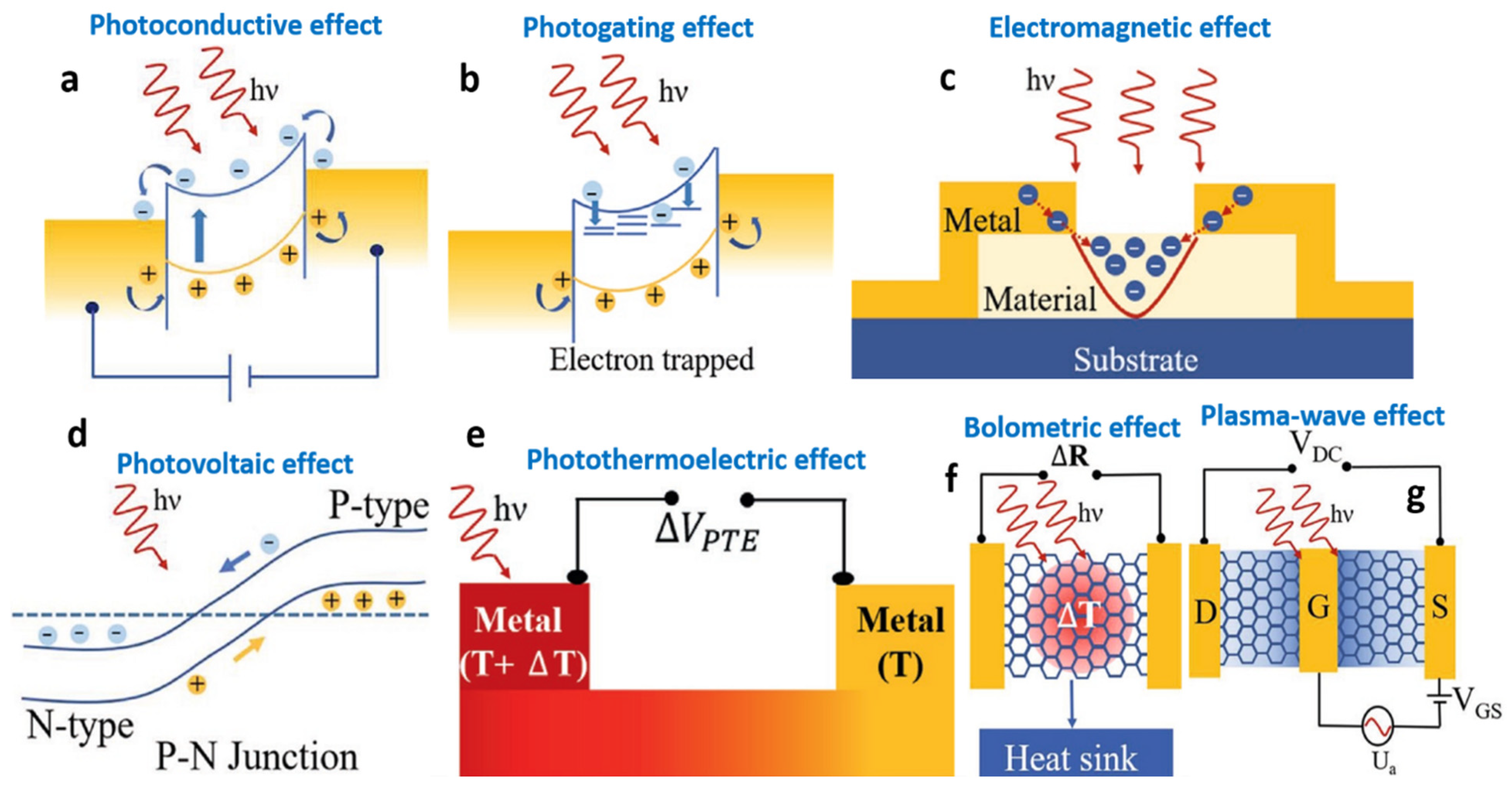
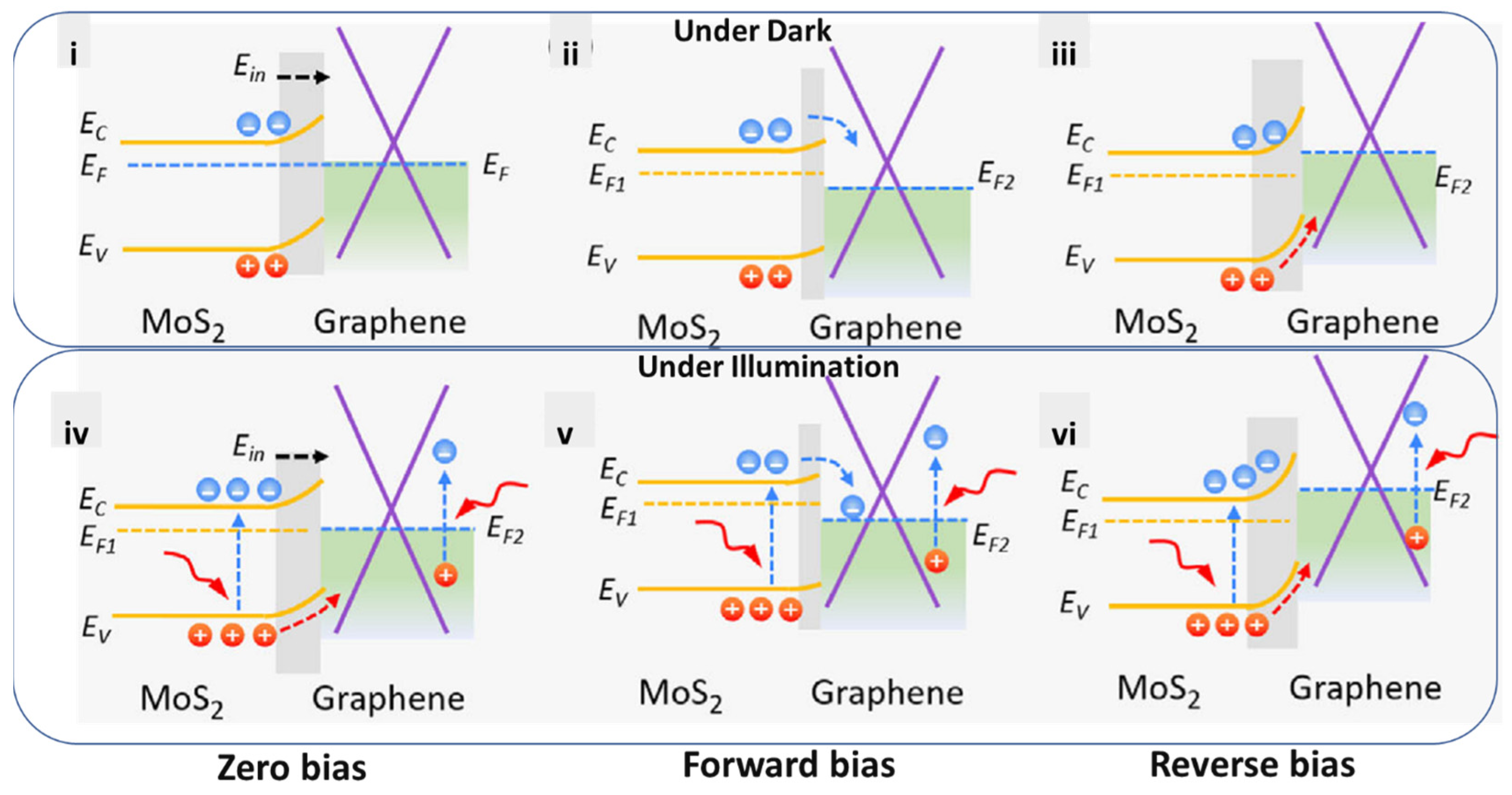
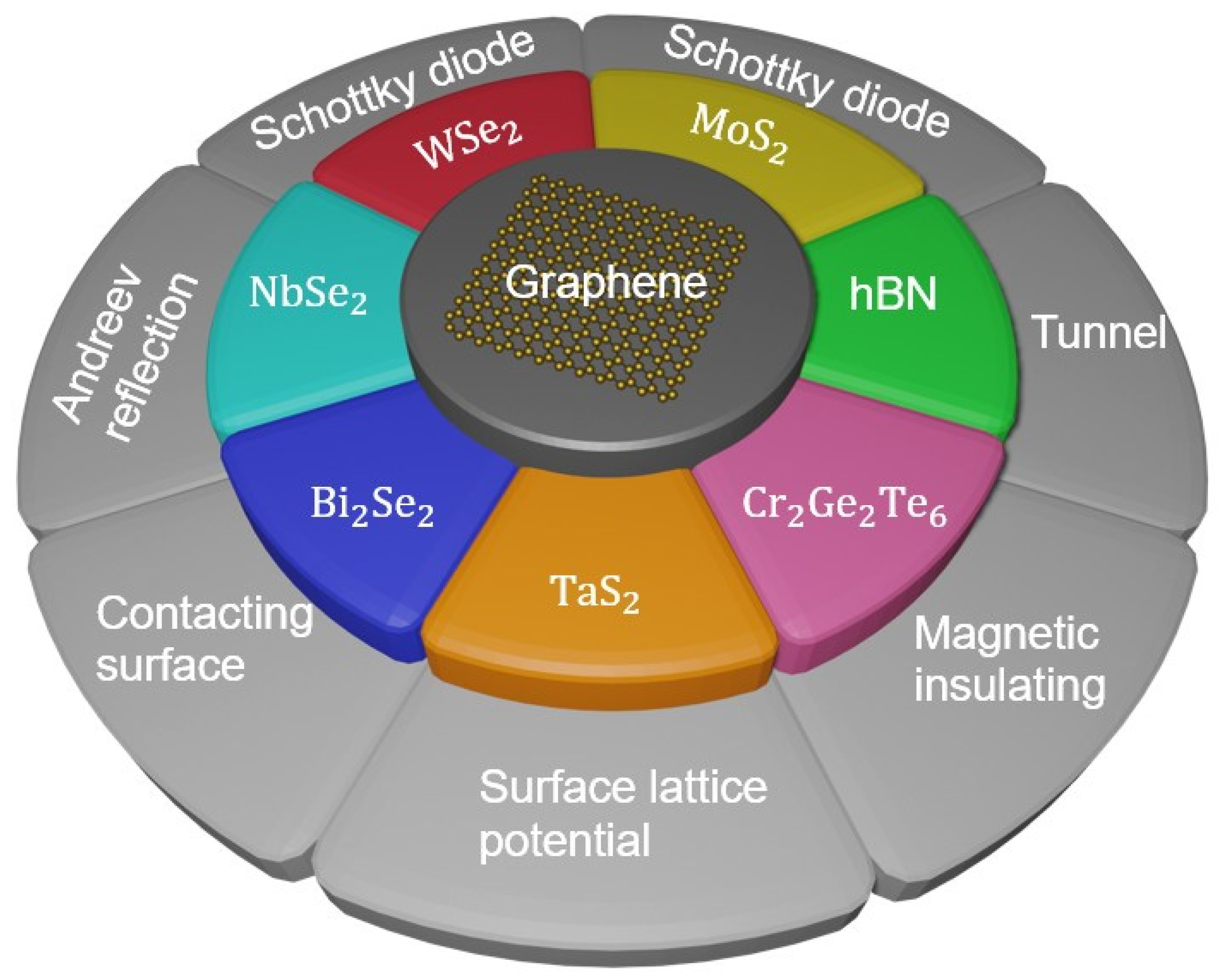
2. Optical Sensing Mechanism of Integrated Graphene Heterostructures
3. Representative Application of Integrated Graphene Heterostructures
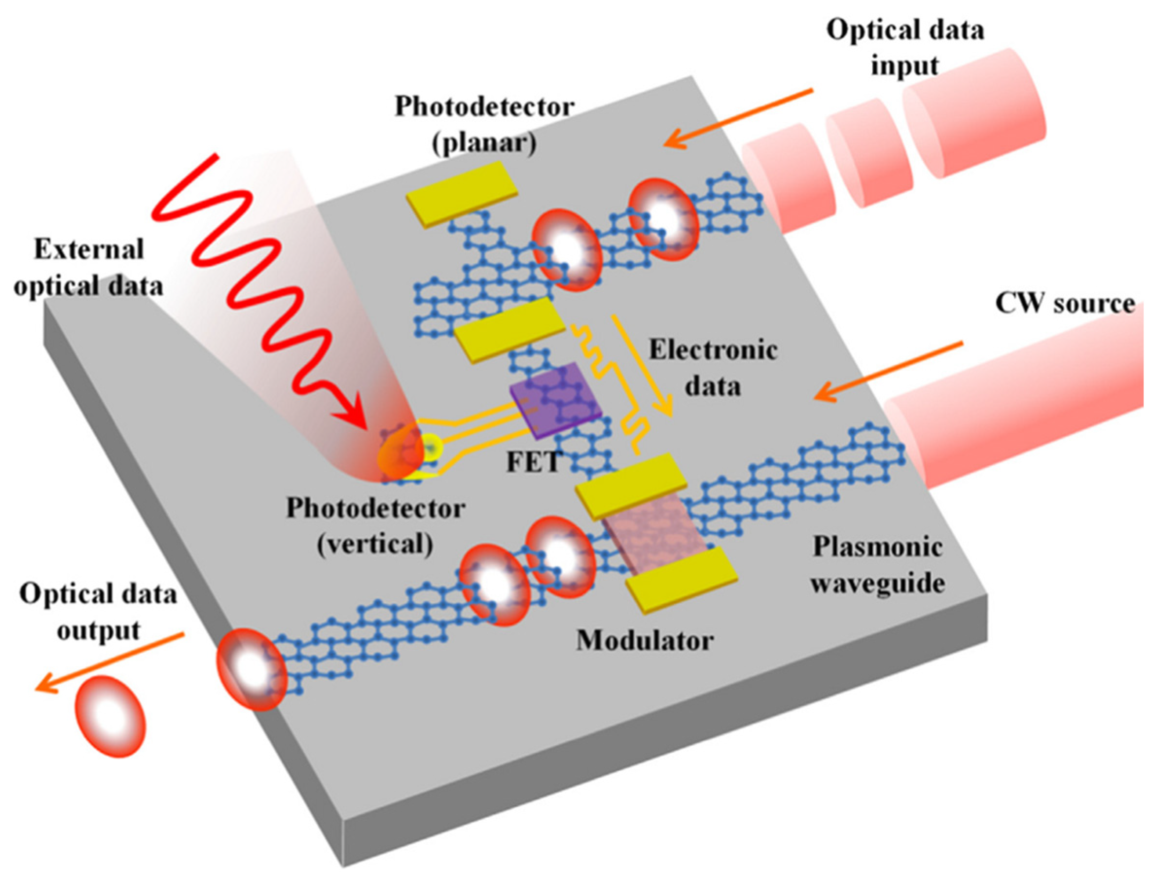
3.1. Ultrafast Optical Sensing Systems
3.2. Plasmonic Systems
3.3. Optical Waveguides and Cavities Systems
3.4. Photonic Crystal (PhC) Sensors Based on PhC Nanocavities and Waveguides
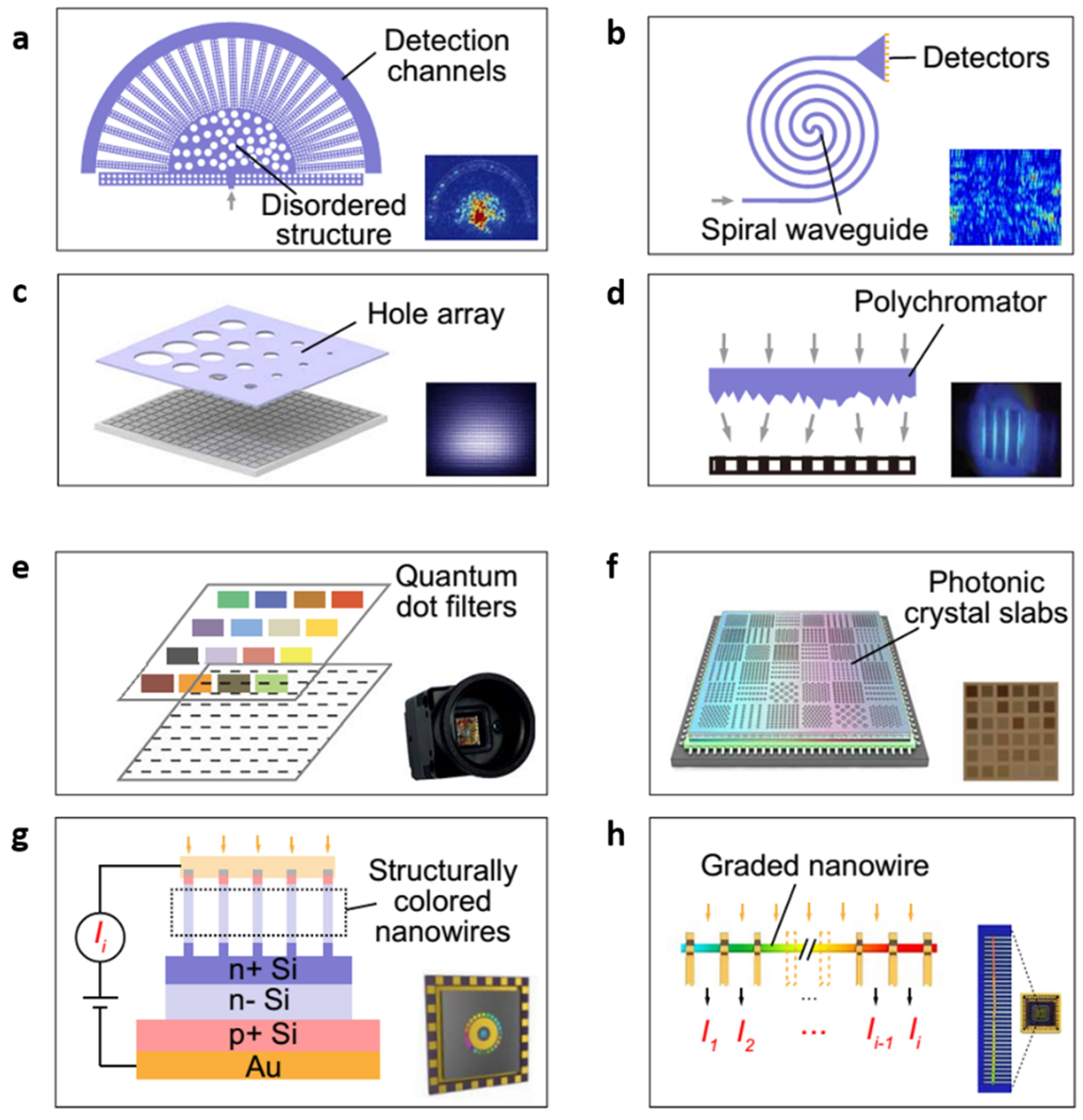
3.5. Optical Spectrometer Systems
3.6. Optical Synaptic Systems
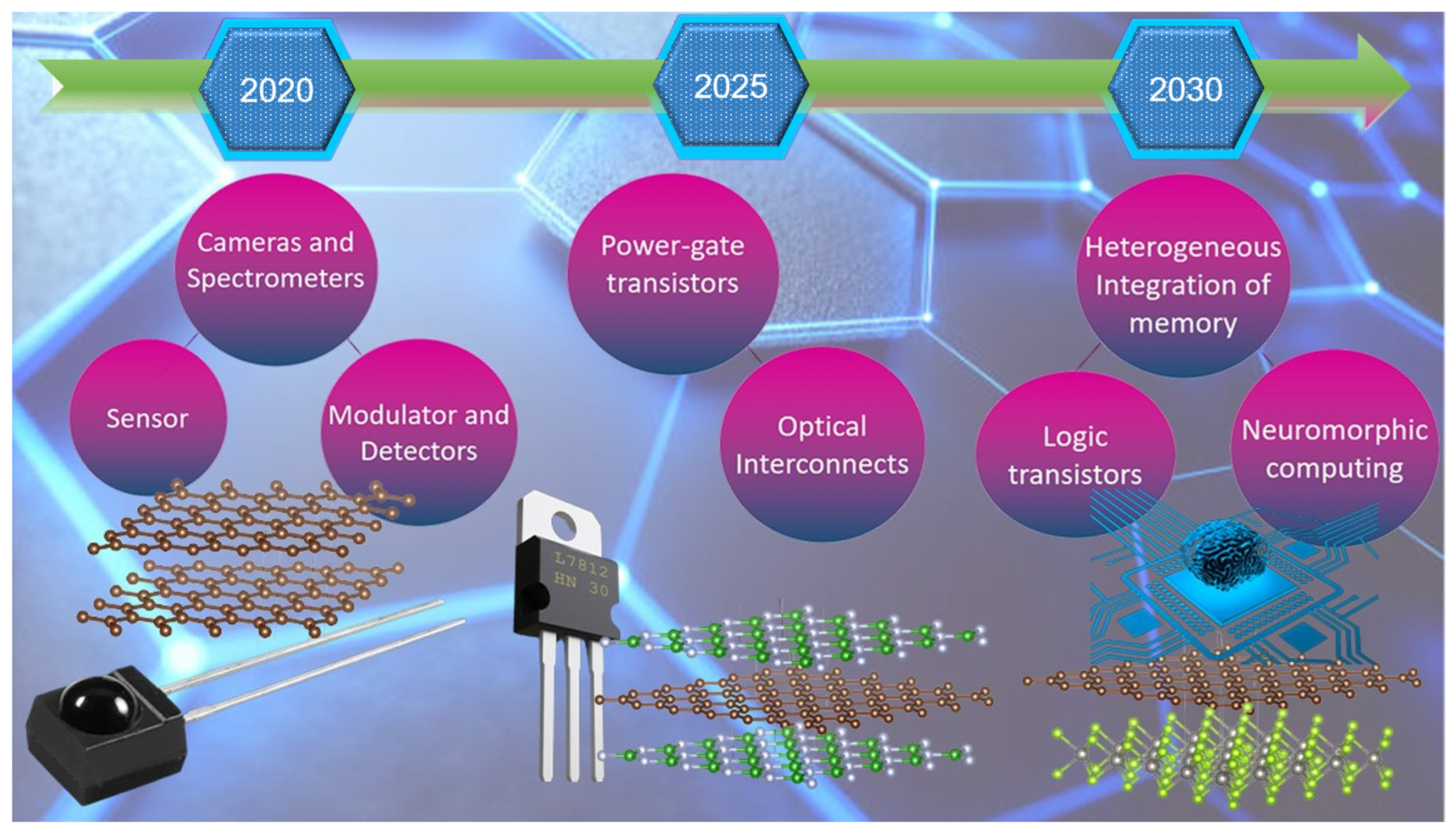
4. Conclusions and Perspectives
Author Contributions
Funding
Data Availability Statement
Conflicts of Interest
Abbreviations
| 1D | One-dimension |
| 2D | Two-dimension |
| 3D | Three-dimension |
| Si | Silicon |
| UV | Ultraviolet |
| IR | Infrared |
| NIR | Near infrared |
| CMOS | Complementary metal-oxide-semiconductor |
| TMDs | Transition metal dichalcogenides |
| NEP | Noise equivalent power |
| Au NPs | Gold nanoparticles |
| rGO | Reduced graphene oxide |
| PhC | Photonic crystal |
| Quality factor | Q-factor |
| TOS | Tungsten oxyselenide |
| ns | Nanosecond |
| ps | Picosecond |
| fJ | Femto-joule |
| BP | Black phosphorous |
| R (λ, D) | Photo-responsivity (the incident light wavelength and the external biasing displacement field) |
| ORRAM | Optoelectronic resistive random-access memory |
| ANN | Artificial neural network |
| CVD | Chemical vapor deposition |
| FEO | Functional electrical optics |
| TENG | Triboelectric nanogenerator |
| vdW | van der Waals |
| TEM | Transmission electron microscopy |
| SEM | Scanning electron microscope |
| STM | Scanning tunneling microscope |
| FTIR | Fourier-transform infrared spectroscopy |
| SAET | Scanning atomic electron tomography |
| PTE | Photo-thermal emission |
| PTI | Photo-thermionic |
| Si-based ICs | Si-based integrated circuits |
| PDs | Photodetectors |
| QDs | Quantum dots |
References
- Rogalski, A.; Kopytko, M.; Martyniuk, P. 2D Material Infrared and Terahertz Detectors: Status and Outlook. Opto-Electron. Rev. 2020, 28, 107–154. [Google Scholar]
- Qiu, Q.; Huang, Z. Photodetectors of 2D Materials from Ultraviolet to Terahertz Waves. Adv. Mater. 2021, 33, 2008126. [Google Scholar] [CrossRef]
- Liu, R.; Wang, F.; Liu, L.; He, X.; Chen, J.; Li, Y.; Zhai, T. Band Alignment Engineering in Two-Dimensional Transition Metal Dichalcogenide-Based Heterostructures for Photodetectors. Small Struct. 2021, 2, 2000136. [Google Scholar] [CrossRef]
- Yao, J.; Yang, G. 2D Material Broadband Photodetectors. Nanoscale 2020, 12, 454–476. [Google Scholar] [CrossRef] [PubMed]
- Aamir Iqbal, M.; Malik, M.; Khac Le, T.; Anwar, N.; Bakhsh, S.; Shahid, W.; Shahid, S.; Irfan, S.; Al-Bahrani, M.; Morsy, K.; et al. Technological Evolution of Image Sensing Designed by Nanostructured Materials. ACS Mater. Lett. 2023, 5, 1027–1060. [Google Scholar] [CrossRef]
- M’Bouana, N.L.P.; Min-Dianey, K.A.A.; Kongnine, D.M.; Rajagopalan, P.; Qadir, A.; Min-Dianey, K.A.; Choi, J.R.; Pham, P.V. Optimization of Gold Square-Shaped Nanopillars Arrays for High-Efficiency Optronics. Opt. Commun. 2022, 512, 128073. [Google Scholar] [CrossRef]
- Min-Dianey, K.A.A.; Le, T.K.; Choi, J.R.; Pham, P. V Advanced Optical Detection through the Use of a Deformably Transferred Nanofilm. Nanomaterials 2021, 11, 816. [Google Scholar] [CrossRef]
- Farooq, U.; Min-Dianey, K.A.A.; Rajagopalan, P.; Malik, M.; Mani Kongnine, D.; Choi, J.R.; Pham, P. V Photodetection Tuning with High Absorptivity Using Stacked 2D Heterostructure Films. Nanomaterials 2022, 12, 712. [Google Scholar] [CrossRef]
- Saran, R.; Curry, R.J. Lead Sulphide Nanocrystal Photodetector Technologies. Nat. Photonics 2016, 10, 81–92. [Google Scholar] [CrossRef]
- Chen, H.; Galili, M.; Verheyen, P.; De Heyn, P.; Lepage, G.; De Coster, J.; Balakrishnan, S.; Absil, P.; Oxenlowe, L.; Van Campenhout, J.; et al. 100-Gbps RZ Data Reception in 67-GHz Si-Contacted Germanium Waveguide p-i-n Photodetectors. J. Light. Technol. 2017, 35, 722–726. [Google Scholar] [CrossRef]
- Liu, C.; Guo, J.; Yu, L.; Li, J.; Zhang, M.; Li, H.; Shi, Y.; Dai, D. Silicon/2D-Material Photodetectors: From near-Infrared to Mid-Infrared. Light Sci. Appli. 2021, 10, 123. [Google Scholar] [CrossRef]
- Gerstner, E. Nobel Prize 2010: Andre Geim & Konstantin Novoselov. Nat. Phys. 2010, 6, 836. [Google Scholar]
- Zhang, Z.; Feng, Y.; Li, F.; Koniakhin, S.; Li, C.; Liu, F.; Zhang, Y.; Xiao, M.; Malpuech, G.; Solnyshkov, D. Angular-Dependent Klein Tunneling in Photonic Graphene. Phys. Rev. Lett. 2022, 129, 233901. [Google Scholar] [CrossRef] [PubMed]
- Xu, M.; Liang, T.; Shi, M.; Chen, H. Graphene-like Two-Dimensional Materials. Chem. Rev. 2013, 113, 3766–3798. [Google Scholar] [CrossRef] [PubMed]
- Nakada, K.; Fujita, M.; Dresselhaus, G.; Dresselhaus, M.S. Edge State in Graphene Ribbons: Nanometer Size Effect and Edge Shape Dependence. Phys. Rev. B 1996, 54, 17954. [Google Scholar] [CrossRef]
- Wakabayashi, K.; Fujita, M.; Ajiki, H.; Sigrist, M. Electronic and Magnetic Properties of Nanographites. Phys. Rev. B 2006, 59, 279–304. [Google Scholar]
- Tian, C.; Miao, W.; Zhao, L.; Wang, J. Graphene Nanoribbons: Current Status and Challenges as Quasi-One-Dimensional Nanomaterials. Rev. Phys. 2023, 10, 100082. [Google Scholar] [CrossRef]
- Pham, P.V.; Bodepudi, S.C.; Shehzad, K.; Liu, Y.; Xu, Y.; Yu, B.; Duan, X. 2D Heterostructures for Ubiquitous Electronics and Optoelectronics: Principles, Opportunities, and Challenges. Chem. Rev. 2022, 122, 6514–6613. [Google Scholar] [CrossRef]
- Du, S.; Lu, W.; Ali, A.; Zhao, P.; Shehzad, K.; Guo, H.; Ma, L.; Liu, X.; Pi, X.; Wang, P.; et al. A Broadband Fluorographene Photodetector. Adv. Mater. 2017, 29, 1700463. [Google Scholar] [CrossRef]
- Wan, X.; Xu, Y.; Guo, H.; Shehzad, K.; Ali, A.; Liu, Y.; Yang, J.; Dai, D.; Lin, C.T.; Liu, L.; et al. A Self-Powered High-Performance Graphene/Silicon Ultraviolet Photodetector with Ultra-Shallow Junction: Breaking the Limit of Silicon? npj 2D Mater. Appl. 2017, 1, 4. [Google Scholar] [CrossRef]
- Liu, W.; Li, L.; Guo, H.; Qadir, A.; Bodepudi, S.C.; Shehzad, K.; Chen, W.; Xie, Y.H.; Wang, X.; Yu, B.; et al. Approaching the Collection Limit in Hot Electron Transistors with Ambipolar Hot Carrier Transport. ACS Nano 2019, 13, 14191–14197. [Google Scholar] [CrossRef] [PubMed]
- Massicotte, M.; Schmidt, P.; Vialla, F.; Schädler, K.G.; Reserbat-Plantey, A.; Watanabe, K.; Taniguchi, T.; Tielrooij, K.J.; Koppens, F.H.L. Picosecond Photoresponse in van Der Waals Heterostructures. Nat. Nanotechnol. 2016, 11, 42–46. [Google Scholar] [CrossRef] [PubMed]
- Li, L.; Wang, J.; Kang, L.; Liu, W.; Yu, L.; Zheng, B.; Brongersma, M.L.; Werner, D.H.; Lan, S.; Shi, Y.; et al. Monolithic Full-Stokes Near-Infrared Polarimetry with Chiral Plasmonic Metasurface Integrated Graphene−Silicon Photodetector. ACS Nano 2020, 14, 16634–16642. [Google Scholar] [CrossRef]
- Zhang, Z.; Lee, Y.; Haque, M.F.; Leem, J.; Hsieh, E.Y.; Nam, S.W. Plasmonic Sensors Based on Graphene and Graphene Hybrid Materials. Nano Converg. 2022, 9, 28. [Google Scholar] [CrossRef] [PubMed]
- Zhang, D.; Du, Y.; Yang, C.; Zeng, P.; Yu, Y.; Xie, Y.; Liang, R.; Ou, Q.; Zhang, S. Tuning Plasmonic Nanostructures in Graphene-Based Nano-Sandwiches Using Ultraviolet/Ozone Functionalization. J. Mater. Sci. 2021, 56, 1359–1372. [Google Scholar] [CrossRef]
- Sriram, P.; Manikandan, A.; Chuang, F.-C.; Chueh, Y.-L. Hybridizing Plasmonic Materials with 2D-Transition Metal Dichalcogenides toward Functional Applications. Small 2020, 16, 1904271. [Google Scholar] [CrossRef]
- Tame, M.S.; McEnery, K.R.; Özdemir, Ş.K.; Lee, J.; Maier, S.A.; Kim, M.S. Quantum Plasmonics. Nat. Phys. 2013, 9, 329–340. [Google Scholar] [CrossRef]
- Clavero, C. Plasmon-Induced Hot-Electron Generation at Nanoparticle/Metal-Oxide Interfaces for Photovoltaic and Photocatalytic Devices. Nat. Photonics 2014, 8, 95–103. [Google Scholar] [CrossRef]
- Polman, A. Applied Physics: Plasmonics Applied. Science 2008, 322, 868–869. [Google Scholar] [CrossRef]
- Liu, Y.; Cheng, R.; Liao, L.; Zhou, H.; Bai, J.; Liu, G.; Liu, L.; Huang, Y.; Duan, X. Plasmon Resonance Enhanced Multicolour Photodetection by Graphene. Nat. Commun. 2011, 2, 577–579. [Google Scholar] [CrossRef]
- Grigorenko, A.N.; Polini, M.; Novoselov, K.S. Graphene Plasmonics. Nat. Photonics 2012, 6, 749–758. [Google Scholar] [CrossRef]
- Abedinpour, S.H.; Vignale, G.; Principi, A.; Polini, M.; Tse, W.K.; Macdonald, A.H. Drude Weight, Plasmon Dispersion, and Ac Conductivity in Doped Graphene Sheets. Phys. Rev. B 2011, 84, 045429. [Google Scholar] [CrossRef]
- Ju, L.; Geng, B.; Horng, J.; Girit, C.; Martin, M.; Hao, Z.; Bechtel, H.A.; Liang, X.; Zettl, A.; Shen, Y.R.; et al. Graphene Plasmonics for Tunable Terahertz Metamaterials. Nat. Nanotechnol. 2011, 6, 630–634. [Google Scholar] [CrossRef] [PubMed]
- Maier, S.A. Plasmonics: Fundamentals and Applications; Springer: Berlin/Heidelberg, Germany, 2007; p. 224. [Google Scholar]
- Yan, H.; Li, X.; Chandra, B.; Tulevski, G.; Wu, Y.; Freitag, M.; Zhu, W.; Avouris, P.; Xia, F. Tunable Infrared Plasmonic Devices Using Graphene/Insulator Stacks. Nat. Nanotechnol. 2012, 7, 330–334. [Google Scholar] [CrossRef] [PubMed]
- Gan, X.; Shiue, R.J.; Gao, Y.; Meric, I.; Heinz, T.F.; Shepard, K.; Hone, J.; Assefa, S.; Englund, D. Chip-Integrated Ultrafast Graphene Photodetector with High Responsivity. Nat. Photonics 2013, 7, 883–887. [Google Scholar] [CrossRef]
- Wang, X.; Cheng, Z.; Xu, K.; Tsang, H.K.; Xu, J. Bin High-Responsivity Graphene/Silicon-Heterostructure Waveguide Photodetectors. Nat. Photonics 2013, 7, 888–891. [Google Scholar] [CrossRef]
- Yin, Y.; Cao, R.; Guo, J.; Liu, C.; Li, J.; Feng, X.; Wang, H.; Du, W.; Qadir, A.; Zhang, H.; et al. High-Speed and High-Responsivity Hybrid Silicon/Black-Phosphorus Waveguide Photodetectors at 2 Μm. Laser Photonics Rev. 2019, 13, 1900032. [Google Scholar] [CrossRef]
- Kim, J.T.; Choe, J.H.; Kim, J.S.; Seo, D.; Kim, Y.D.; Chung, K.H. Graphene-Based Plasmonic Waveguide Devices for Electronic-Photonic Integrated Circuit. Opt. Laser Technol. 2018, 106, 76–86. [Google Scholar] [CrossRef]
- Guo, J.; Li, J.; Liu, C.; Yin, Y.; Wang, W.; Ni, Z.; Fu, Z.; Yu, H.; Xu, Y.; Shi, Y.; et al. High-Performance Silicon−graphene Hybrid Plasmonic Waveguide Photodetectors beyond 1.55 Μm. Light Sci. Appl. 2020, 9, 29. [Google Scholar] [CrossRef]
- Gan, X.; Mak, K.F.; Gao, Y.; You, Y.; Hatami, F.; Hone, J.; Heinz, T.F.; Englund, D. Strong Enhancement of Light-Matter Interaction in Graphene Coupled to a Photonic Crystal Nanocavity. Nano Lett. 2012, 12, 5626–5631. [Google Scholar] [CrossRef]
- Yablonovitch, E. Inhibited Spontaneous Emission in Solid-State Physics and Electronics. Phys. Rev. Lett. 1987, 58, 2059–2062. [Google Scholar] [CrossRef] [PubMed]
- John, S. Strong Localization of Photons in Certain Disordered Dielectric Superlattices. Phys. Rev. Lett. 1987, 58, 2486–2489. [Google Scholar] [CrossRef] [PubMed]
- Zhang, Y.N.; Zhao, Y.; Lv, R.Q. A Review for Optical Sensors Based on Photonic Crystal Cavities. Sens. Actuators A Phys. 2015, 233, 374–389. [Google Scholar] [CrossRef]
- Kassa-Baghdouche, L. Optical Properties of a Point-Defect Nanocavity-Based Elliptical-Hole Photonic Crystal for Mid-Infrared Liquid Sensing. Phys. Scr. 2020, 95, 5035–5040. [Google Scholar] [CrossRef]
- Lalanne, P.; Sauvan, C.; Hugonin, J.P. Photon Confinement in Photonic Crystal Nanocavities. Laser Photonics Rev. 2008, 2, 514–526. [Google Scholar] [CrossRef]
- Song, B.-S.; Asano, T.; Noda, S.; Akahane, Y. Fine-Tuned High-Q Photonic-Crystal Nanocavity. Opt. Express 2005, 13, 1202–1214. [Google Scholar]
- Chakravarty, S.; Hosseini, A.; Xu, X.; Zhu, L.; Zou, Y.; Chen, R.T. Analysis of Ultra-High Sensitivity Configuration in Chip-Integrated Photonic Crystal Microcavity Bio-Sensors. Appl. Phys. Lett. 2014, 104, 191109. [Google Scholar] [CrossRef]
- Takata, K.; Takata, K.; Takata, K.; Kuramochi, E.; Kuramochi, E.; Shinya, A.; Shinya, A.; Notomi, M.; Notomi, M.; Notomi, M.; et al. Improved Design and Experimental Demonstration of Ultrahigh-Q C6-Symmetric H1 Hexapole Photonic Crystal Nanocavities. Opt. Express 2023, 31, 11864–11884. [Google Scholar] [CrossRef]
- Asano, T.; Tanaka, Y.; Takahashi, Y.; Noda, S.; Nakamura, T. Improvement in the Quality Factors for Photonic Crystal Nanocavities via Visualization of the Leaky Components. Opt. Express 2016, 24, 9541–9549. [Google Scholar]
- Kassa-Baghdouche, L.; Cassan, E. Mid-Infrared Refractive Index Sensing Using Optimized Slotted Photonic Crystal Waveguides. Photonics Nanostruct.-Fundam. Appl. 2018, 28, 32–36. [Google Scholar] [CrossRef]
- Liu, M.; Yin, X.; Ulin-Avila, E.; Geng, B.; Zentgraf, T.; Ju, L.; Wang, F.; Zhang, X. A Graphene-Based Broadband Optical Modulator. Nature 2011, 474, 64–67. [Google Scholar] [CrossRef] [PubMed]
- Xu, Q.; Schmidt, B.; Pradhan, S.; Lipson, M. Micrometre-Scale Silicon Electro-Optic Modulator. Nature 2005, 435, 325–327. [Google Scholar] [CrossRef]
- Gao, Y.; Shiue, R.J.; Gan, X.; Li, L.; Peng, C.; Meric, I.; Wang, L.; Szep, A.; Walker, D.; Hone, J.; et al. High-Speed Electro-Optic Modulator Integrated with Graphene-Boron Nitride Heterostructure and Photonic Crystal Nanocavity. Nano Lett. 2015, 15, 2001–2005. [Google Scholar] [CrossRef]
- Choi, M.S.; Nipane, A.; Kim, B.S.Y.; Ziffer, M.E.; Datta, I.; Borah, A.; Jung, Y.; Kim, B.; Rhodes, D.; Jindal, A.; et al. High Carrier Mobility in Graphene Doped Using a Monolayer of Tungsten Oxyselenide. Nat. Electron. 2021, 4, 731–739. [Google Scholar] [CrossRef]
- Wolffenbuttel, R.F. State-of-the-Art in Integrated Optical Microspectrometers. IEEE Trans. Instrum. Meas. 2004, 53, 197–202. [Google Scholar] [CrossRef]
- Redding, B.; Liew, S.F.; Sarma, R.; Cao, H. Compact Spectrometer Based on a Disordered Photonic Chip. Nat. Photonics 2013, 7, 746–751. [Google Scholar] [CrossRef]
- Redding, B.; Fatt Liew, S.; Bromberg, Y.; Sarma, R.; Cao, H. Evanescently Coupled Multimode Spiral Spectrometer. Optica 2016, 3, 956. [Google Scholar] [CrossRef]
- Xu, C.; Hong, X.; Zhu, Y.; Wang, Q.; Chen, Y.; Huang, W.; Li, X.; Yang, T.; Ho, H.; Zhou, X.; et al. Miniature Spectrometer Based on Diffraction in a Dispersive Hole Array. Opt. Lett. 2015, 40, 3217–3220. [Google Scholar]
- Menon, R.; Wang, P. Computational Spectrometer Based on a Broadband Diffractive Optic. Opt. Express 2014, 22, 14575–14587. [Google Scholar]
- Bao, J.; Bawendi, M.G. A Colloidal Quantum Dot Spectrometer. Nature 2015, 523, 67–70. [Google Scholar] [CrossRef]
- Wang, Z.; Yi, S.; Chen, A.; Zhou, M.; Luk, T.S.; James, A.; Nogan, J.; Ross, W.; Joe, G.; Shahsafi, A.; et al. Single-Shot on-Chip Spectral Sensors Based on Photonic Crystal Slabs. Nat. Commun. 2019, 10, 1020. [Google Scholar] [CrossRef] [PubMed]
- Meng, J.; Cadusch, J.J.; Crozier, K.B. Detector-Only Spectrometer Based on Structurally Colored Silicon Nanowires and a Reconstruction Algorithm. Nano Lett. 2020, 20, 320–328. [Google Scholar] [CrossRef] [PubMed]
- Yang, Z.; Albrow-Owen, T.; Cui, H.; Alexander-Webber, J.; Gu, F.; Wang, X.; Wu, T.C.; Zhuge, M.; Williams, C.; Wang, P.; et al. Single-Nanowire Spectrometers. Science 2019, 365, 1017–1020. [Google Scholar] [CrossRef]
- Yang, Z.; Albrow-Owen, T.; Cai, W.; Hasan, T. Miniaturization of Optical Spectrometers. Science 2021, 371, eabe0722. [Google Scholar] [CrossRef] [PubMed]
- Manzardo, O.; Herzig, H.P.; Marxer, C.R.; de Rooij, N.F. Miniaturized Time-Scanning Fourier Transform Spectrometer Based on Silicon Technology. Opt. Lett. 1999, 24, 1705–1707. [Google Scholar] [CrossRef]
- Zhang, H.; Wang, X.L.; Soos, J.I.; Crisp, J.A. Design of a Miniature Solid State NIR Spectrometer. Proc. SPIE 1995, 2475, 376–383. [Google Scholar]
- Sander, D.; Müller, J. Selffocussing Phase Transmission Grating for an Integrated Optical Microspectrometer. Sens. Actuators A Phys. 2001, 88, 1–9. [Google Scholar] [CrossRef]
- Yuan, S.; Naveh, D.; Watanabe, K.; Taniguchi, T.; Xia, F. A Wavelength-Scale Black Phosphorus Spectrometer. Nat. Photonics 2021, 15, 601–607. [Google Scholar] [CrossRef]
- Shrestha, V.R.; Craig, B.; Meng, J.; Bullock, J.; Javey, A.; Crozier, K.B. Mid- to Long-Wave Infrared Computational Spectroscopy with a Graphene Metasurface Modulator. Sci. Rep. 2020, 10, 5377. [Google Scholar] [CrossRef]
- Seo, S.; Jo, S.H.; Kim, S.; Shim, J.; Oh, S.; Kim, J.H.; Heo, K.; Choi, J.W.; Choi, C.; Oh, S.; et al. Artificial Optic-Neural Synapse for Colored and Color-Mixed Pattern Recognition. Nat. Commun. 2018, 9, 5106. [Google Scholar] [CrossRef]
- Shainline, J.M. Optoelectronic Intelligence. Appl. Phys. Lett. 2021, 118, 160501. [Google Scholar] [CrossRef]
- Qian, C.; Oh, S.; Choi, Y.; Kim, J.H.; Sun, J.; Huang, H.; Yang, J.; Gao, Y.; Park, J.H.; Cho, J.H. Solar-Stimulated Optoelectronic Synapse Based on Organic Heterojunction with Linearly Potentiated Synaptic Weight for Neuromorphic Computing. Nano Energy 2019, 66, 104095. [Google Scholar] [CrossRef]
- Huang, W.; Hang, P.; Wang, Y.; Wang, K.; Han, S.; Chen, Z.; Peng, W.; Zhu, Y.; Xu, M.; Zhang, Y.; et al. Zero-Power Optoelectronic Synaptic Devices. Nano Energy 2020, 73, 104790. [Google Scholar] [CrossRef]
- Zhou, F.; Zhou, Z.; Chen, J.; Choy, T.H.; Wang, J.; Zhang, N.; Lin, Z.; Yu, S.; Kang, J.; Wong, H.S.P.; et al. Optoelectronic Resistive Random Access Memory for Neuromorphic Vision Sensors. Nat. Nanotechnol. 2019, 14, 776–782. [Google Scholar] [CrossRef]
- Qin, S.; Wang, F.; Liu, Y.; Wan, Q.; Wang, X.; Xu, Y.; Shi, Y.; Wang, X.; Zhang, R. A Light-Stimulated Synaptic Device Based on Graphene Hybrid Phototransistor. 2D Mater. 2017, 4, 035022. [Google Scholar] [CrossRef]
- Ni, Z.; Wang, Y.; Liu, L.; Zhao, S.; Xu, Y.; Pi, X.; Yang, D. Hybrid Structure of Silicon Nanocrystals and 2D WSe2 for Broadband Optoelectronic Synaptic Devices. In Proceedings of the 2018 IEEE International Electron Devices Meeting (IEDM), San Francisco, CA, USA, 1–5 December 2018; pp. 887–890. [Google Scholar]
- Mennel, L.; Symonowicz, J.; Wachter, S.; Polyushkin, D.K.; Molina-Mendoza, A.J.; Mueller, T. Ultrafast Machine Vision with 2D Material Neural Network Image Sensors. Nature 2020, 579, 62–66. [Google Scholar] [CrossRef]
- Wang, Y.; Yin, L.; Huang, W.; Li, Y.; Huang, S.; Zhu, Y.; Yang, D.; Pi, X. Optoelectronic Synaptic Devices for Neuromorphic Computing. Adv. Intell. Syst. 2021, 3, 2000099. [Google Scholar] [CrossRef]
- Luo, Z.D.; Xia, X.; Yang, M.M.; Wilson, N.R.; Gruverman, A.; Alexe, M. Artificial Optoelectronic Synapses Based on Ferroelectric Field-Effect Enabled 2D Transition Metal Dichalcogenide Memristive Transistors. ACS Nano 2020, 14, 746–754. [Google Scholar] [CrossRef]
- Meng, Y.; Li, F.; Lan, C.; Bu, X.; Kang, X.; Wei, R.; Yip, S.P.; Li, D.; Wang, F.; Takahashi, T.; et al. Artificial Visual Systems Enabled by Quasi-Two-Dimensional Electron Gases in Oxide Superlattice Nanowires. Sci. Adv. 2020, 6, eabc6389. [Google Scholar] [CrossRef]
- Yu, J.; Yang, X.; Gao, G.; Xiong, Y.; Wang, Y.; Han, J.; Chen, Y.; Zhang, H.; Sun, Q.; Wang, Z.L. Bioinspired Mechano-Photonic Artificial Synapse Based on Graphene/MoS2 Heterostructure. Sci. Adv. 2021, 7, eabd9117. [Google Scholar] [CrossRef]
- Seo, S.; Lee, J.-J.; Lee, R.-G.; Kim, H.; Park, S.; Jung, S.; Lee, H.-K.; Andreev, M.; Lee, K.-B.; Jung, K.-S.; et al. An Optogenetics-Inspired Flexible van Der Waals Optoelectronic Synapse and Its Application to a Convolutional Neural Network. Adv. Mater. 2021, 33, 102980. [Google Scholar] [CrossRef]
- Sun, J.; Oh, S.; Choi, Y.; Seo, S.; Oh, M.J.; Lee, M.; Lee, W.B.; Yoo, P.J.; Cho, J.H.; Park, J.H. Optoelectronic Synapse Based on IGZO-Alkylated Graphene Oxide Hybrid Structure. Adv. Func. Mater. 2018, 28, 1804397. [Google Scholar] [CrossRef]
- Han, X.; Song, P.; Xing, J.; Chen, Z.; Li, D.; Xu, G.; Zhao, X.; Ma, F.; Rong, D.; Shi, Y.; et al. High-Performance Phototransistors Based on MnPSe3 and Its Hybrid Structures with Au Nanoparticles. ACS Appl. Mater. Interfaces 2021, 13, 2836–2844. [Google Scholar] [CrossRef] [PubMed]
- Li, Y.; Wang, Y.; Yin, L.; Huang, W.; Peng, W.; Zhu, Y.; Wang, K.; Yang, D.; Pi, X. Silicon-Based Inorganic-Organic Hybrid Optoelectronic Synaptic Devices Simulating Cross-Modal Learning. Sc. China Inf. Sci. 2021, 64, 162401. [Google Scholar] [CrossRef]
- Yin, L.; Pi, X.; Yang, D. Silicon-Based Optoelectronic Synaptic Devices. Chin. Phys. B 2020, 29, 070703. [Google Scholar] [CrossRef]
- Callicó, G.M. Graphene: Image Sensors Go Broadband. Nat. Photonics 2017, 11, 332–333. [Google Scholar] [CrossRef]
- Goossens, S.; Navickaite, G.; Monasterio, C.; Gupta, S.; Piqueras, J.J.; Pérez, R.; Burwell, G.; Nikitskiy, I.; Lasanta, T.; Galán, T.; et al. Broadband Image Sensor Array Based on Graphene-CMOS Integration. Nat. Photonics 2017, 11, 366–371. [Google Scholar] [CrossRef]
- Ko, T.J.; Li, H.; Mofid, S.A.; Yoo, C.; Okogbue, E.; Han, S.S.; Shawkat, M.S.; Krishnaprasad, A.; Islam, M.M.; Dev, D.; et al. Two-Dimensional Near-Atom-Thickness Materials for Emerging Neuromorphic Devices and Applications. iScience 2020, 23, 101676. [Google Scholar] [CrossRef]
- Chen, X.; Shehzad, K.; Gao, L.; Long, M.; Guo, H.; Qin, S.; Wang, X.; Wang, F.; Shi, Y.; Hu, W.; et al. Graphene Hybrid Structures for Integrated and Flexible Optoelectronics. Adv. Mater. 2020, 32, 1902039. [Google Scholar] [CrossRef]
- Zhou, X.; Hu, X.; Yu, J.; Liu, S.; Shu, Z.; Zhang, Q.; Li, H.; Ma, Y.; Xu, H.; Zhai, T. 2D Layered Material-based van Der Waals Heterostructures for Optoelectronics. Adv. Func. Mater. 2018, 28, 1706587. [Google Scholar] [CrossRef]
- Kundu, B.; Mohanty, P.; Kumar, P.; Nayak, B.; Mahato, B.; Ranjan, P.; Chakraborty, S.K.; Sahoo, S.; Sahoo, P.K. Synthesis of Lateral Heterostructure of 2D Materials for Optoelectronic Devices: Challenges and Opportunities. Emergent Mater. 2021, 4, 923–949. [Google Scholar] [CrossRef]
- Wu, M.; Zhang, Z.; Xu, X.; Zhang, Z.; Duan, Y.; Dong, J.; Qiao, R.; You, S.; Wang, L.; Qi, J.; et al. Seeded Growth of Large Single-Crystal Copper Foils with High-Index Facets. Nature 2020, 581, 406–410. [Google Scholar] [CrossRef]
- Chuang, F.C.; Lin, W.H.; Huang, Z.Q.; Hsu, C.H.; Kuo, C.C.; Ozolins, V.; Yeh, V. Electronic Structures of an Epitaxial Graphene Monolayer on SiC(0001) after Gold Intercalation: A First-Principles Study. Nanotechnology 2011, 22, 275704. [Google Scholar] [CrossRef]
- Hsu, C.H.; Ozolins, V.; Chuang, F.C. First-Principles Study of Bi and Sb Intercalated Graphene on SiC(0001) Substrate. Surf. Sci. 2013, 616, 149–154. [Google Scholar] [CrossRef]
- Tian, X.; Kim, D.S.; Yang, S.; Ciccarino, C.J.; Gong, Y.; Yang, Y.; Yang, Y.; Duschatko, B.; Yuan, Y.; Ajayan, P.M.; et al. Correlating the Three-Dimensional Atomic Defects and Electronic Properties of Two-Dimensional Transition Metal Dichalcogenides. Nat. Mater. 2020, 19, 867–873. [Google Scholar] [CrossRef]
- Akinwande, D.; Huyghebaert, C.; Wang, C.H.; Serna, M.I.; Goossens, S.; Li, L.J.; Wong, H.S.P.; Koppens, F.H.L. Graphene and Two-Dimensional Materials for Silicon Technology. Nature 2019, 573, 507–518. [Google Scholar] [CrossRef]
- Liu, Y.; Huang, Y.; Duan, X. Van Der Waals Integration before and beyond Two-Dimensional Materials. Nature 2019, 567, 323–333. [Google Scholar] [CrossRef]
- Quellmalz, A.; Wang, X.; Sawallich, S.; Uzlu, B.; Otto, M.; Wagner, S.; Wang, Z.; Prechtl, M.; Hartwig, O.; Luo, S.; et al. Large-Area Integration of Two-Dimensional Materials and Their Heterostructures by Wafer Bonding. Nat. Commun. 2021, 12, 917. [Google Scholar] [CrossRef]
- Patel, H.; Huang, L.; Kim, C.J.; Park, J.; Graham, M.W. Stacking Angle-Tunable Photoluminescence from Interlayer Exciton States in Twisted Bilayer Graphene. Nat. Commun. 2019, 10, 1445. [Google Scholar] [CrossRef]
- Liao, M.; Wei, Z.; Du, L.; Wang, Q.; Tang, J.; Yu, H.; Wu, F.; Zhao, J.; Xu, X.; Han, B.; et al. Precise Control of the Interlayer Twist Angle in Large Scale MoS2 Homostructures. Nat. Commun. 2020, 11, 2153. [Google Scholar] [CrossRef]
- Jago, R.; Malic, E.; Wendler, F. Microscopic Origin of the Bolometric Effect in Graphene. Phys. Rev. B 2019, 99, 035419. [Google Scholar] [CrossRef]
- Britnell, L.; Ribeiro, R.M.; Eckmann, A.; Jalil, R.; Belle, B.D.; Mishchenko, A.; Kim, Y.J.; Gorbachev, R.V.; Georgiou, T.; Morozov, S.V.; et al. Strong Light-Matter Interactions in Heterostructures of Atomically Thin Films. Science 2013, 340, 1311–1314. [Google Scholar] [CrossRef] [PubMed]
- Betz, A.C.; Vialla, F.; Brunel, D.; Voisin, C.; Picher, M.; Cavanna, A.; Madouri, A.; Fève, G.; Berroir, J.M.; Plaçais, B.; et al. Hot Electron Cooling by Acoustic Phonons in Graphene. Phys. Rev. Lett. 2012, 109, 056805. [Google Scholar] [CrossRef] [PubMed]
- Trushin, M. Theory of Thermionic Emission from a Two-Dimensional Conductor and Its Application to a Graphene-Semiconductor Schottky Junction. Appl. Phys. Lett. 2018, 112, 171109. [Google Scholar] [CrossRef]
- Massicotte, M.; Schmidt, P.; Vialla, F.; Watanabe, K.; Taniguchi, T.; Tielrooij, K.J.; Koppens, F.H.L. Photo-Thermionic Effect in Vertical Graphene Heterostructures. Nat. Commun. 2016, 7, 12174. [Google Scholar] [CrossRef]
- Ma, Q.; Andersen, T.I.; Nair, N.L.; Gabor, N.M.; Massicotte, M.; Lui, C.H.; Young, A.F.; Fang, W.; Watanabe, K.; Taniguchi, T.; et al. Tuning Ultrafast Electron Thermalization Pathways in a van der Waals Heterostructure. Nat. Phys. 2016, 12, 455–460. [Google Scholar] [CrossRef]
- Liao, L.; Lin, Y.C.; Bao, M.; Cheng, R.; Bai, J.; Liu, Y.; Qu, Y.; Wang, K.L.; Huang, Y.; Duan, X. High-Speed Graphene Transistors with a Self-Aligned Nanowire Gate. Nature 2010, 467, 305–308. [Google Scholar] [CrossRef]
- Liao, L.; Bai, J.; Cheng, R.; Lin, Y.C.; Jiang, S.; Qu, Y.; Huang, Y.; Duan, X. Sub-100 nm Channel Length Graphene Transistors. Nano Lett. 2010, 10, 3952–3956. [Google Scholar] [CrossRef]
- Cheng, R.; Bai, J.; Liao, L.; Zhou, H.; Chen, Y.; Liu, L.; Lin, Y.C.; Jiang, S.; Huang, Y.; Duan, X. High-Frequency Self-Aligned Graphene Transistors with Transferred Gate Stacks. Proc. Natl. Acad. Sci. USA 2012, 109, 11588–11592. [Google Scholar] [CrossRef]
- Werner, T.; Vianello; Bichler, O.; Grossi, A.; Nowak, E.; Nodin, J.F.; Yvert, B.; Desalvo, B.; Perniola, L. Experimental Demonstration of Short and Long Term Synaptic Plasticity Using OxRAM Multi K-Bit Arrays for Reliable Detection in Highly Noisy Input Data. In Proceedings of the 2016 IEEE International Electron Devices Meeting (IEDM), San Francisco, CA, USA, 3–7 December 2016; pp. 432–435. [Google Scholar]
- Yadav, S.; Jena, S.R.; M.B., B.; Altaee, A.; Saxena, M.; Samal, A.K. Heterostructures of 2D Materials-Quantum Dots (QDs) for Optoelectronic Devices: Challenges and Opportunities. Emergent Mater. 2021, 4, 901–922. [Google Scholar] [CrossRef]
- Gu, L.; Poddar, S.; Lin, Y.; Long, Z.; Zhang, D.; Zhang, Q.; Shu, L.; Qiu, X.; Kam, M.; Javey, A.; et al. A Biomimetic Eye with a Hemispherical Perovskite Nanowire Array Retina. Nature 2020, 581, 278–282. [Google Scholar] [CrossRef]
- Yang, R.; Huang, H.M.; Guo, X. Memristive Synapses and Neurons for Bioinspired Computing. Adv. Mater. Technol. 2019, 5, 1900287. [Google Scholar] [CrossRef]
- Chen, H.; Liu, C.; Wu, Z.; He, Y.; Wang, Z.; Zhang, H.; Wan, Q.; Hu, W.; Zhang, D.W.; Liu, M.; et al. Time-Tailoring van Der Waals Heterostructures for Human Memory System Programming. Adv. Sci. 2019, 6, 1901072. [Google Scholar] [CrossRef]
- Zhang, X.; Grajal, J.; Vazquez-Roy, J.L.; Radhakrishna, U.; Wang, X.; Chern, W.; Zhou, L.; Lin, Y.; Shen, P.C.; Ji, X.; et al. Two-Dimensional MoS2-Enabled Flexible Rectenna for Wi-Fi-Band Wireless Energy Harvesting. Nature 2019, 566, 368–372. [Google Scholar] [CrossRef]
- Schaibley, J.R.; Yu, H.; Clark, G.; Rivera, P.; Ross, J.S.; Seyler, K.L.; Yao, W.; Xu, X. Valleytronics in 2D Materials. Nat. Rev. Mater. 2016, 1, 16055. [Google Scholar] [CrossRef]
- Mak, K.F.; Xiao, D.; Shan, J. Light–Valley Interactions in 2D Semiconductors. Nat. Photonics 2018, 12, 451–460. [Google Scholar] [CrossRef]
- Li, L.; Shao, L.; Liu, X.; Gao, A.; Wang, H.; Zheng, B.; Hou, G.; Shehzad, K.; Yu, L.; Miao, F.; et al. Room-Temperature Valleytronic Transistor. Nat. Nanotechnol. 2020, 15, 743–749. [Google Scholar] [CrossRef]
- Yang, Y.; Li, J.; Yin, J.; Xu, S.; Mullan, C.; Taniguchi, T.; Watanabe, K.; Geim, A.K.; Novoselov, K.S.; Mishchenko, A. In Situ Manipulation of van Der Waals Heterostructures for Twistronics. Sci. Adv. 2020, 6, eabd3655. [Google Scholar] [CrossRef]
- Xu, C.; Balents, L. Topological Superconductivity in Twisted Multilayer Graphene. Phys. Rev. Lett. 2018, 121, 087001. [Google Scholar] [CrossRef]
- Liu, J.; Ma, Z.; Gao, J.; Dai, X. Quantum Valley Hall Effect, Orbital Magnetism, and Anomalous Hall Effect in Twisted Multilayer Graphene Systems. Phys. Rev. X 2019, 9, 031021. [Google Scholar] [CrossRef]
- Bistritzer, R.; Macdonald, A.H. Moiré Bands in Twisted Double-Layer Graphene. Proc. Natl. Acad. Sci. USA 2011, 108, 12233–12237. [Google Scholar] [CrossRef] [PubMed]
- Arora, H.S.; Polski, R.; Zhang, Y.; Thomson, A.; Choi, Y.; Kim, H.; Lin, Z.; Wilson, I.Z.; Xu, X.; Chu, J.H.; et al. Superconductivity in Metallic Twisted Bilayer Graphene Stabilized by WSe2. Nature 2020, 583, 379–384. [Google Scholar] [CrossRef] [PubMed]
- Wong, D.; Nuckolls, K.P.; Oh, M.; Lian, B.; Xie, Y.; Jeon, S.; Watanabe, K.; Taniguchi, T.; Bernevig, B.A.; Yazdani, A. Cascade of Electronic Transitions in Magic-Angle Twisted Bilayer Graphene. Nature 2020, 582, 198–202. [Google Scholar] [CrossRef] [PubMed]
- Carr, S.; Fang, S.; Kaxiras, E. Electronic-Structure Methods for Twisted Moiré Layers. Nat. Rev. Mater. 2020, 5, 748–763. [Google Scholar] [CrossRef]
- Andersen, T.I.; Scuri, G.; Sushko, A.; De Greve, K.; Sung, J.; Zhou, Y.; Wild, D.S.; Gelly, R.J.; Heo, H.; Bérubé, D.; et al. Excitons in a Reconstructed Moiré Potential in Twisted WSe2/WSe2 Homobilayers. Nat. Mater. 2021, 20, 480–487. [Google Scholar] [CrossRef]
- Ahn, E.C. 2D Materials for Spintronic Devices. npj 2D Mater. Appl. 2020, 4, 17. [Google Scholar] [CrossRef]
- Lu, J.W.; Chen, E.; Kabir, M.; Stan, M.R.; Wolf, S.A. Spintronics Technology: Past, Present and Future. Int. Mater. Rev. 2016, 61, 456–472. [Google Scholar] [CrossRef]
- Tan, H.; Ni, Z.; Peng, W.; Du, S.; Liu, X.; Zhao, S.; Li, W.; Ye, Z.; Xu, M.; Xu, Y.; et al. Broadband Optoelectronic Synaptic Devices Based on Silicon Nanocrystals for Neuromorphic Computing. Nano Energy 2018, 52, 422–430. [Google Scholar] [CrossRef]
- Sun, L.; Wang, W.; Yang, H. Recent Progress in Synaptic Devices Based on 2D Materials. Adv. Intell. Syst. 2020, 2, 1900167. [Google Scholar] [CrossRef]
- Yin, L.; Han, C.; Zhang, Q.; Ni, Z.; Zhao, S.; Wang, K.; Li, D.; Xu, M.; Wu, H.; Pi, X.; et al. Synaptic Silicon-Nanocrystal Phototransistors for Neuromorphic Computing. Nano Energy 2019, 63, 103859. [Google Scholar] [CrossRef]
- Ren, Y.; Hu, L.; Mao, J.Y.; Yuan, J.; Zeng, Y.J.; Ruan, S.; Yang, J.Q.; Zhou, L.; Zhou, Y.; Han, S.T. Phosphorene Nano-Heterostructure Based Memristors with Broadband Response Synaptic Plasticity. J. Mater. Chem. C 2018, 6, 9383–9393. [Google Scholar] [CrossRef]
- Xu, Z.; Li, F.; Wu, C.; Ma, F.; Zheng, Y.; Yang, K.; Chen, W.; Hu, H.; Guo, T.; Kim, T.W. Ultrathin Electronic Synapse Having High Temporal/Spatial Uniformity and an Al2O3/Graphene Quantum Dots/Al2O3 Sandwich Structure for Neuromorphic Computing. NPG Asia Mater. 2019, 11, 18. [Google Scholar] [CrossRef]
- Kumar, M.; Ban, D.K.; Kim, S.M.; Kim, J.; Wong, C.P. Vertically Aligned WS2 Layers for High-Performing Memristors and Artificial Synapses. Adv. Electron. Mater. 2019, 5, 1900467. [Google Scholar] [CrossRef]
- Seo, S.; Kang, B.-S.; Lee, J.-J.; Ryu, H.-J.; Kim, S.; Kim, H.; Oh, S.; Shim, J.; Heo, K.; Oh, S.; et al. Artificial van der Waals Hybrid Synapse and Its Application to Acoustic Pattern Recognition. Nat. Commun. 2020, 11, 3936. [Google Scholar] [CrossRef]
- Chen, H.; Xue, X.; Liu, C.; Fang, J.; Wang, Z.; Wang, J.; Zhang, D.W.; Hu, W.; Zhou, P. Logic Gates Based on Neuristors Made from Two-Dimensional Materials. Nat. Electron. 2021, 4, 399–404. [Google Scholar] [CrossRef]


Disclaimer/Publisher’s Note: The statements, opinions and data contained in all publications are solely those of the individual author(s) and contributor(s) and not of MDPI and/or the editor(s). MDPI and/or the editor(s) disclaim responsibility for any injury to people or property resulting from any ideas, methods, instructions or products referred to in the content. |
© 2023 by the authors. Licensee MDPI, Basel, Switzerland. This article is an open access article distributed under the terms and conditions of the Creative Commons Attribution (CC BY) license (https://creativecommons.org/licenses/by/4.0/).
Share and Cite
Pham, P.V.; Mai, T.-H.; Do, H.-B.; Ponnusamy, V.K.; Chuang, F.-C. Integrated Graphene Heterostructures in Optical Sensing. Micromachines 2023, 14, 1060. https://doi.org/10.3390/mi14051060
Pham PV, Mai T-H, Do H-B, Ponnusamy VK, Chuang F-C. Integrated Graphene Heterostructures in Optical Sensing. Micromachines. 2023; 14(5):1060. https://doi.org/10.3390/mi14051060
Chicago/Turabian StylePham, Phuong V., The-Hung Mai, Huy-Binh Do, Vinoth Kumar Ponnusamy, and Feng-Chuan Chuang. 2023. "Integrated Graphene Heterostructures in Optical Sensing" Micromachines 14, no. 5: 1060. https://doi.org/10.3390/mi14051060