
Simulation of a Fully Digital Computing-in-Memory for Non-Volatile Memory for Artificial Intelligence Edge Applications

Abstract
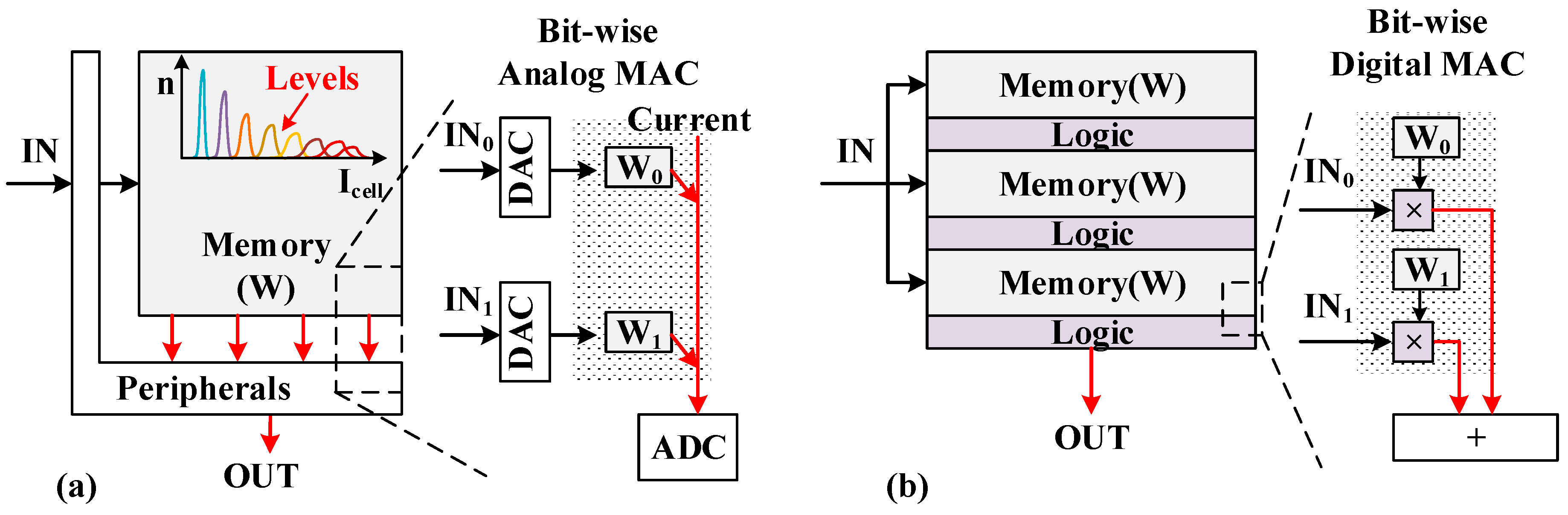
:1. Introduction
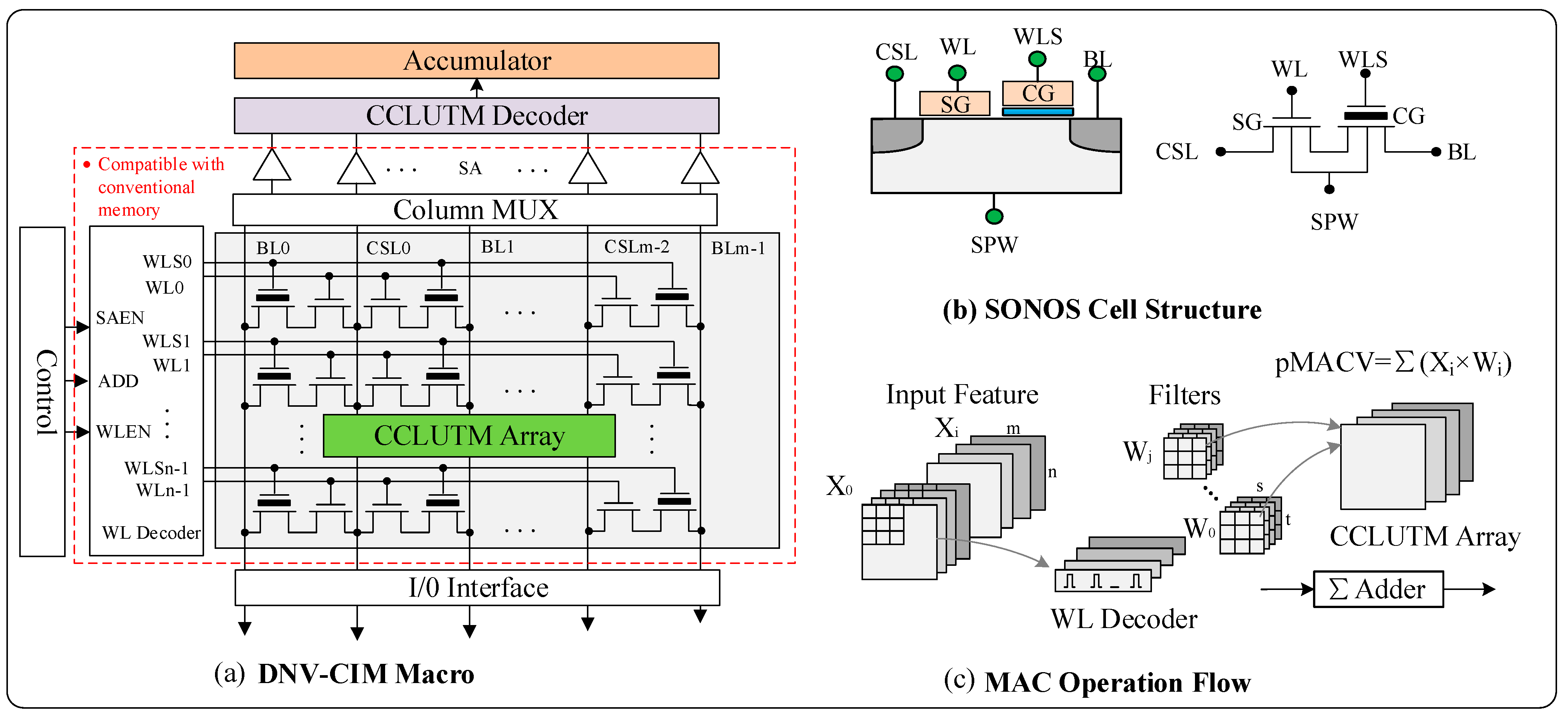
2. Overall Structure of the Proposed DNV-CIM Macro
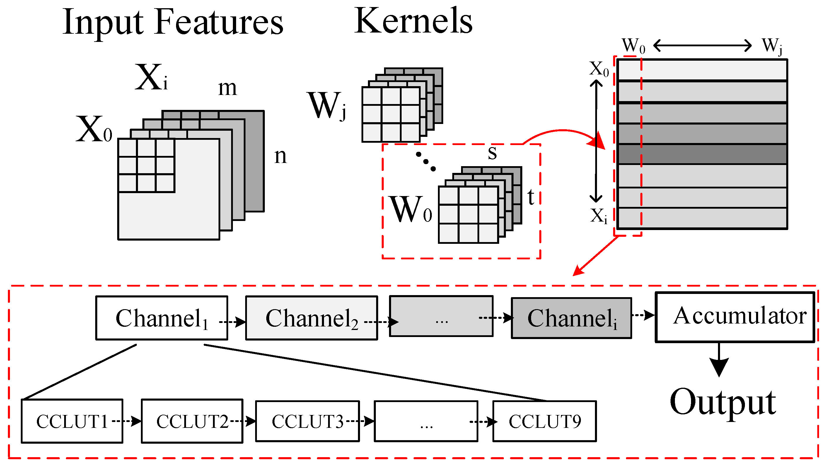
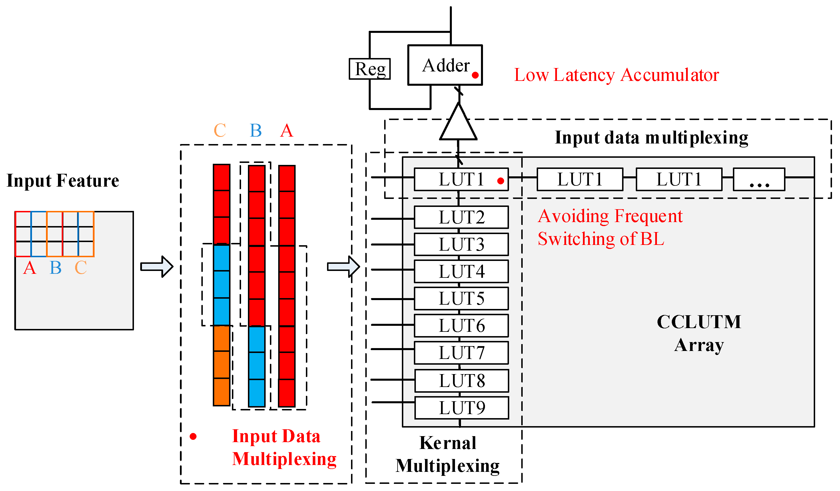
3. CCLUTM
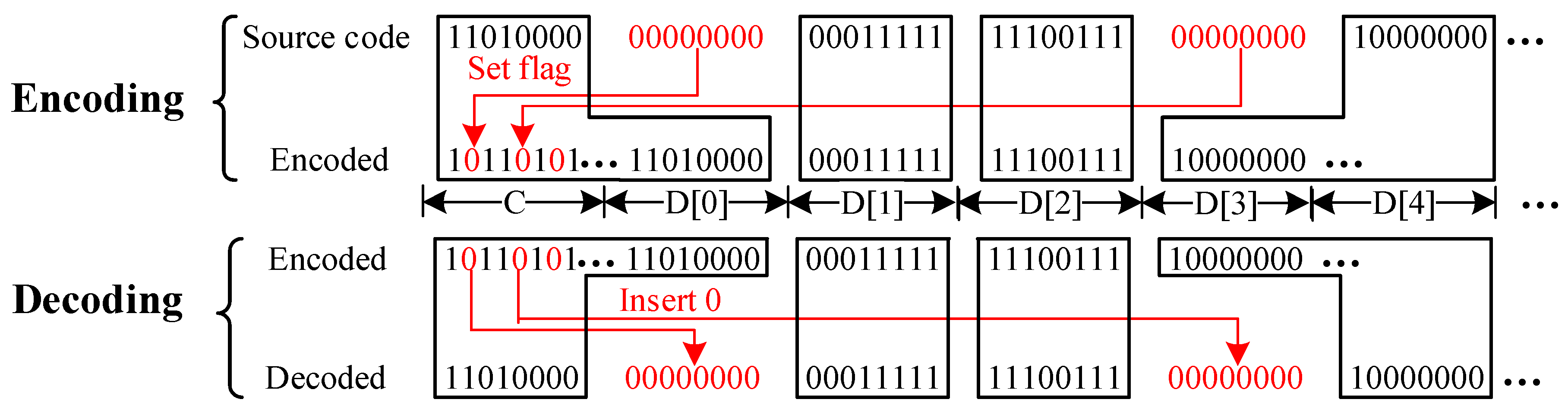
4. Continuous Accumulation Scheme
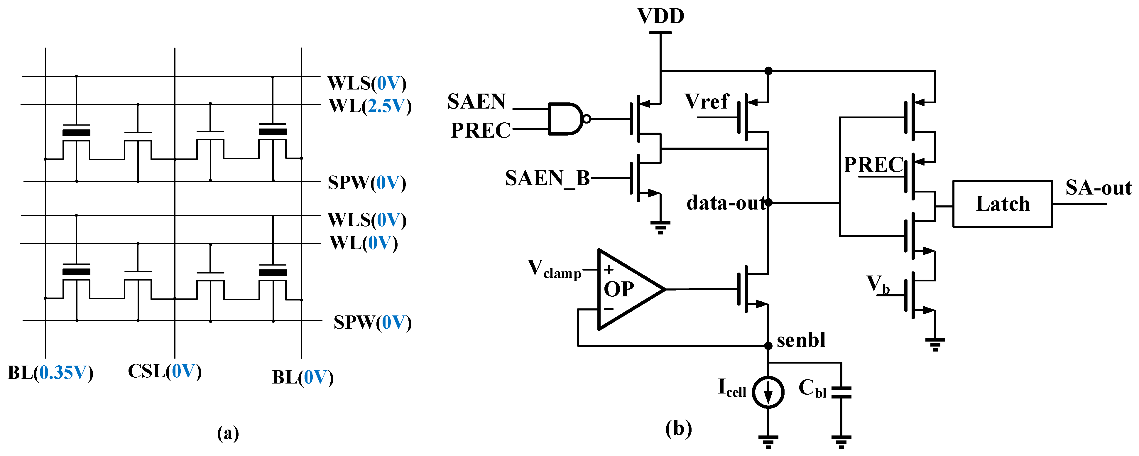
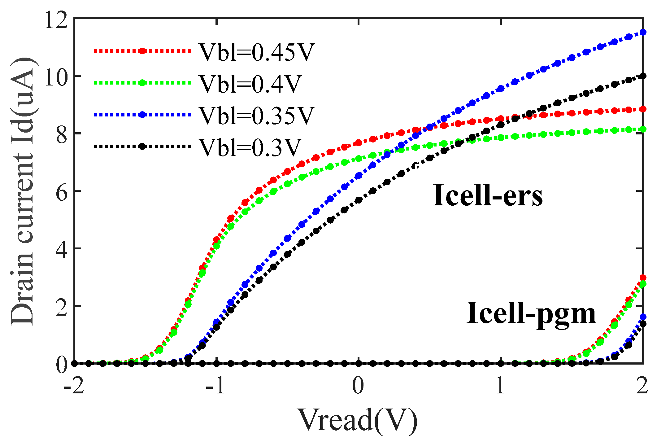
5. Experiment
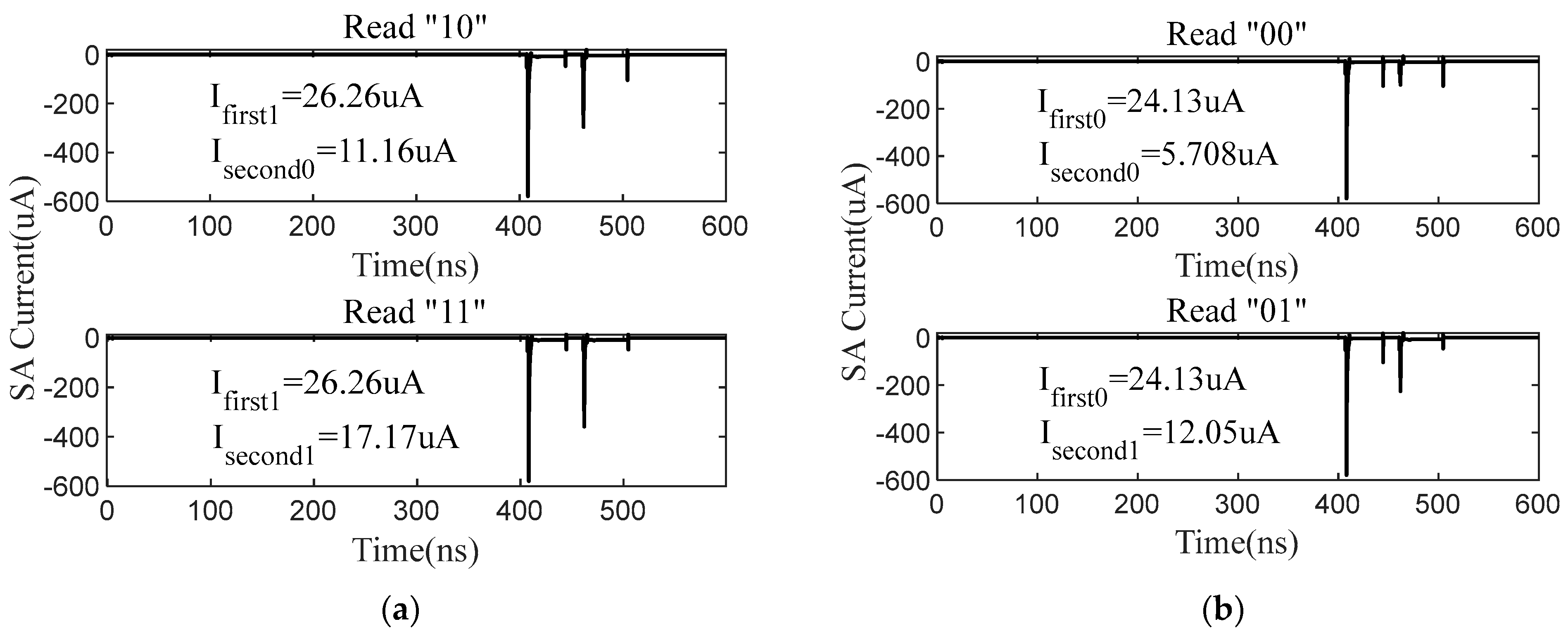
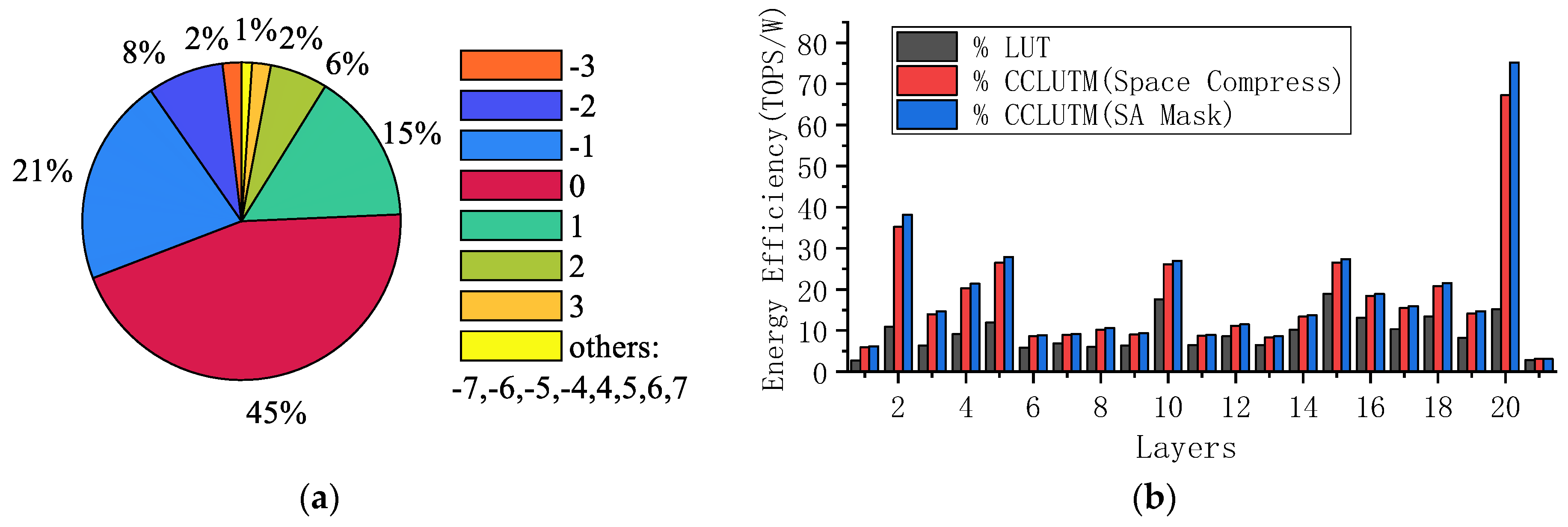
6. Results
7. Conclusions
Author Contributions
Funding
Conflicts of Interest
References
- Huang, K.; Ha, Y.; Zhao, R.; Kumar, A.; Lian, Y. A Low Active Leakage and High Reliability Phase Change Memory (PCM) Based Non-Volatile FPGA Storage Element. IEEE Trans. Circuits Syst. I Regul. Pap. 2014, 61, 2605–2613. [Google Scholar] [CrossRef]
- Yin, S.; Kim, Y.; Han, X.; Barnaby, H.; Yu, S.; Luo, Y.; He, W.; Sun, X.; Kim, J.-J.; Seo, J.-S. Monolithically Integrated RRAM- and CMOS-Based In-Memory Computing Optimizations for Efficient Deep Learning. IEEE Micro 2019, 39, 54–63. [Google Scholar] [CrossRef]
- Wang, Z.; Li, C.; Lin, P.; Rao, M.; Nie, Y.; Song, W.; Qiu, Q.; Li, Y.; Yan, P.; Strachan, J.P.; et al. In situ training of feed-forward and recurrent convolutional memristor networks. Nat. Mach. Intell. 2019, 1, 434–442. [Google Scholar] [CrossRef]
- Xiao, T.P.; Feinberg, B.; Bennett, C.H.; Agrawal, V.; Saxena, P.; Prabhakar, V.; Ramkumar, K.; Medu, H.; Raghavan, V.; Chettuvetty, R.; et al. An Accurate, Error-Tolerant, and Energy-Efficient Neural Network Inference Engine Based on SONOS Analog Memory. IEEE Trans. Circuits Syst. I Regul. Pap. 2022, 69, 1480–1493. [Google Scholar]
- Han, R.; Huang, P.; Xiang, Y.; Liu, C.; Dong, Z.; Su, Z.; Liu, Y.; Liu, L.; Liu, X.; Kang, J. A Novel Convolution Computing Paradigm Based on NOR Flash Array With High Computing Speed and Energy Efficiency. IEEE Trans. Circuits Syst. I Regul. Pap. 2019, 66, 1692–1703. [Google Scholar] [CrossRef]
- Lee, C.-F.; Lu, C.-H.; Lee, C.-E.; Mori, H.; Fujiwara, H.; Shih, Y.-C.; Chou, T.-L.; Chih, Y.-D.; Chang, T.-Y.J. A 12nm 121-TOPS/W 41.6-TOPS/mm2 All Digital Full Precision SRAM-based Compute-in-Memory with Configurable Bit-width For AI Edge Applications. In Proceedings of the 2022 IEEE Symposium on VLSI Technology and Circuits (VLSI Technology and Circuits), Honolulu, HI, USA, 12–17 June 2022; pp. 24–25. [Google Scholar]
- Fujiwara, H.; Mori, H.; Zhao, W.-C.; Chuang, M.-C.; Naous, R.; Chuang, C.-K.; Hashizume, T.; Sun, D.; Lee, C.-F.; Akarvardar, K.; et al. A 5-nm 254-TOPS/W 221-TOPS/mm2 Fully-Digital Computing-in-Memory Macro Supporting Wide-Range Dynamic-Voltage-Frequency Scaling and Simultaneous MAC and Write Operations. In Proceedings of the 2022 IEEE International Solid-State Circuits Conference (ISSCC), San Francisco, CA, USA, 20–26 February 2022; Volume 65, pp. 1–3. [Google Scholar]
- Yan, B.; Hsu, J.-L.; Yu, P.-C.; Lee, C.-C.; Zhang, Y.; Yue, W.; Mei, G.; Yang, Y.; Yang, Y.; Li, H.; et al. A 1.041-Mb/mm2 27.38-TOPS/W Signed-INT8 Dynamic-Logic-Based ADC-less SRAM Compute-in-Memory Macro in 28nm with Reconfigurable Bitwise Operation for AI and Embedded Applications. In Proceedings of the 2022 IEEE International Solid-State Circuits Conference (ISSCC), San Francisco, CA, USA, 20–26 February 2022; Volume 65, pp. 188–190. [Google Scholar]
- Wu, P.-C.; Su, J.-W.; Chung, Y.-L.; Hong, L.-Y.; Ren, J.-S.; Chang, F.-C.; Wu, Y.; Chen, H.-Y.; Lin, C.-H.; Hsiao, H.-M.; et al. A 28 nm 1 Mb Time-Domain Computing-in-Memory 6T-SRAM Macro with a 6.6ns Latency, 1241GOPS and 37.01TOPS/W for 8b-MAC Operations for Edge-AI Devices. In Proceedings of the 2022 IEEE International Solid-State Circuits Conference (ISSCC), San Francisco, CA, USA, 20–26 February 2022; Volume 65, pp. 1–3. [Google Scholar]
- Zhu, H.; Jiao, B.; Zhang, J.; Jia, X.; Wang, Y.; Guan, T.; Wang, S.; Niu, D.; Zheng, H.; Chen, C.; et al. COMB-MCM: Computing-on-Memory-Boundary NN Processor with Bipolar Bitwise Sparsity Optimization for Scalable Multi-Chiplet-Module Edge Machine Learning. In Proceedings of the 2022 IEEE International Solid-State Circuits Conference (ISSCC), San Francisco, CA, USA, 20–26 February 2022; Volume 65, pp. 1–3. [Google Scholar]
- Han, S.; Mao, H.; Dally, W.J. Deep Compression: Compressing Deep Neural Network with Pruning, Trained Quantization and Huffman Coding. arXiv 2015, arXiv:1510.00149. [Google Scholar]
- Sze, V.; Chen, Y.H.; Yang, T.J.; Emer, J.S. Efficient Processing of Deep Neural Networks. In Synthesis Lectures on Computer Architecture; Morgan & Claypool Publishers: Kentfield, CA, USA, 2020. [Google Scholar]
- Liu, R.; Peng, X.; Sun, X.; Khwa, W.-S.; Si, X.; Chen, J.-J.; Li, J.-F.; Chang, M.-F.; Yu, S. Parallelizing SRAM Arrays with Customized Bit-Cell for Binary Neural Networks. In Proceedings of the 2018 55th ACM/ESDA/IEEE Design Automation Conference (DAC), San Francisco, CA, USA, 24–29 June 2018; pp. 1–6. [Google Scholar]
- Zhang, Y.; Zeng, S.; Zhu, Z.; Qin, Z.; Wang, C.; Li, J.; Zhang, S.; He, Y.; Dou, C.; Si, X.; et al. A 40 nm 1 Mb 35.6 TOPS/W MLC NOR-Flash Based Computation-in-Memory Structure for Machine Learning. In Proceedings of the 2021 IEEE International Symposium on Circuits and Systems (ISCAS), Daegu, Republic of Korea, 22–28 May 2021; pp. 1–5. [Google Scholar]
- Xiang, Y.C.; Huang, P.; Zhou, Z.; Han, R.Z.; Jiang, Y.N.; Shu, Q.M.; Su, Z.Q.; Liu, Y.B.; Liu, X.Y.; Kang, J.F. Analog Deep Neural Network Based on NOR Flash Computing Array for High Speed/Energy Efficiency Computation. In Proceedings of the 2019 IEEE International Symposium on Circuits and Systems (ISCAS), Sapporo, Japan, 26–29 May 2019; pp. 1–4. [Google Scholar]


| Decoding Method | |
|---|---|
| C [0] = 0 | |
| C [0] = 1 | |
| C [1] = 0 | |
| C [1] = 1 | |
| C [n] = 0 | |
| C [n] = 1 | |
| WL Length | 128 | 256 | 512 | 1024 | 2048 |
|---|---|---|---|---|---|
| Time/ns | 6 | 6.4 | 7.9 | 10.9 | 26 |
| Current/μA | 8.3 | 10.9 | 15.3 | 25.2 | 42.5 |
| DAC [13] | TCAS-I [5] | TCAS-I [4] | ISCAS [15] | ISCAS [14] | This Work | |
|---|---|---|---|---|---|---|
| Technology Node | 65 nm | - | 40 nm | 65 nm | 40 nm | 40 nm |
| Memory Capacity | 4 Kb | 64 Kb | 512 kb | 1 Mb | 1 Mb | 8 Mb |
| Accelerate Type | Digital SRAM | Analog (SLC NOR Flash) | Analog (MLC NOR Flash) | Analog (MLC NOR Flash) | Analog (MLC NOR Flash) | Digital (SLC NOR Flash) |
| Data Resolution | 1 bit | 1 bit | 8 bit | 4 bit | 4 bit | 4 bit |
| Energy Efficiency (TOPS/W) | >50 (1 b/1 b) (BNN) | - (BNN) | 20.1 (4 b/4 b) (ResNet50) | - BSIM3v3 | 35.6 (4 b/4 b) (peak) (VGG-16) | 75.18 (4 b/4 b) 67.25 (4 b/4 b) (peak) (ResNet18) |
| Accuracy | 87.46% | - | 74.3% (loss 2.16%) | 97.1% (loss 0.7%) | 92.73% | 93.04% |
Disclaimer/Publisher’s Note: The statements, opinions and data contained in all publications are solely those of the individual author(s) and contributor(s) and not of MDPI and/or the editor(s). MDPI and/or the editor(s) disclaim responsibility for any injury to people or property resulting from any ideas, methods, instructions or products referred to in the content. |
© 2023 by the authors. Licensee MDPI, Basel, Switzerland. This article is an open access article distributed under the terms and conditions of the Creative Commons Attribution (CC BY) license (https://creativecommons.org/licenses/by/4.0/).
Share and Cite
Hu, H.; Feng, C.; Zhou, H.; Dong, D.; Pan, X.; Wang, X.; Zhang, L.; Cheng, S.; Pang, W.; Liu, J. Simulation of a Fully Digital Computing-in-Memory for Non-Volatile Memory for Artificial Intelligence Edge Applications. Micromachines 2023, 14, 1175. https://doi.org/10.3390/mi14061175
Hu H, Feng C, Zhou H, Dong D, Pan X, Wang X, Zhang L, Cheng S, Pang W, Liu J. Simulation of a Fully Digital Computing-in-Memory for Non-Volatile Memory for Artificial Intelligence Edge Applications. Micromachines. 2023; 14(6):1175. https://doi.org/10.3390/mi14061175
Chicago/Turabian StyleHu, Hongyang, Chuancai Feng, Haiyang Zhou, Danian Dong, Xiaoshan Pan, Xiwei Wang, Lu Zhang, Shuaiqi Cheng, Wan Pang, and Jing Liu. 2023. "Simulation of a Fully Digital Computing-in-Memory for Non-Volatile Memory for Artificial Intelligence Edge Applications" Micromachines 14, no. 6: 1175. https://doi.org/10.3390/mi14061175
APA StyleHu, H., Feng, C., Zhou, H., Dong, D., Pan, X., Wang, X., Zhang, L., Cheng, S., Pang, W., & Liu, J. (2023). Simulation of a Fully Digital Computing-in-Memory for Non-Volatile Memory for Artificial Intelligence Edge Applications. Micromachines, 14(6), 1175. https://doi.org/10.3390/mi14061175