
Plasma Figure Correction Method Based on Multiple Distributed Material Removal Functions
 ,
,
Abstract
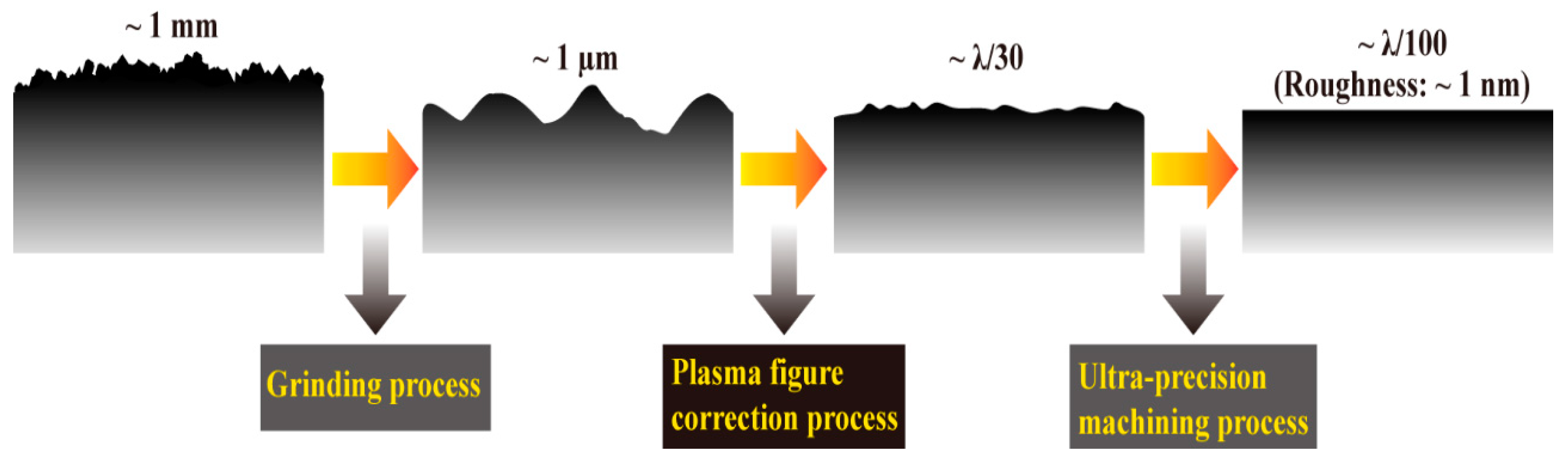
:1. Introduction
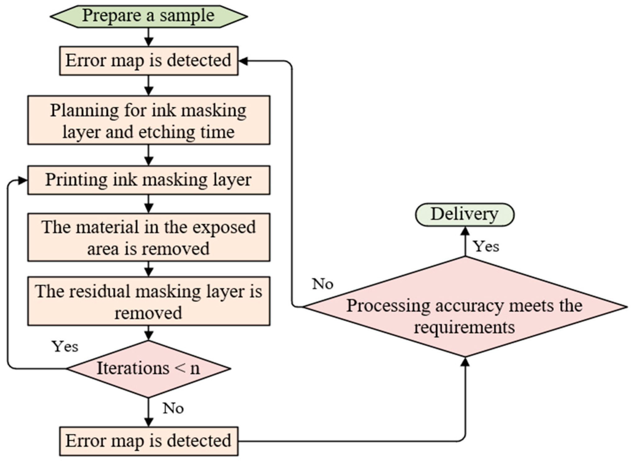
2. Theory and Mathematical Model
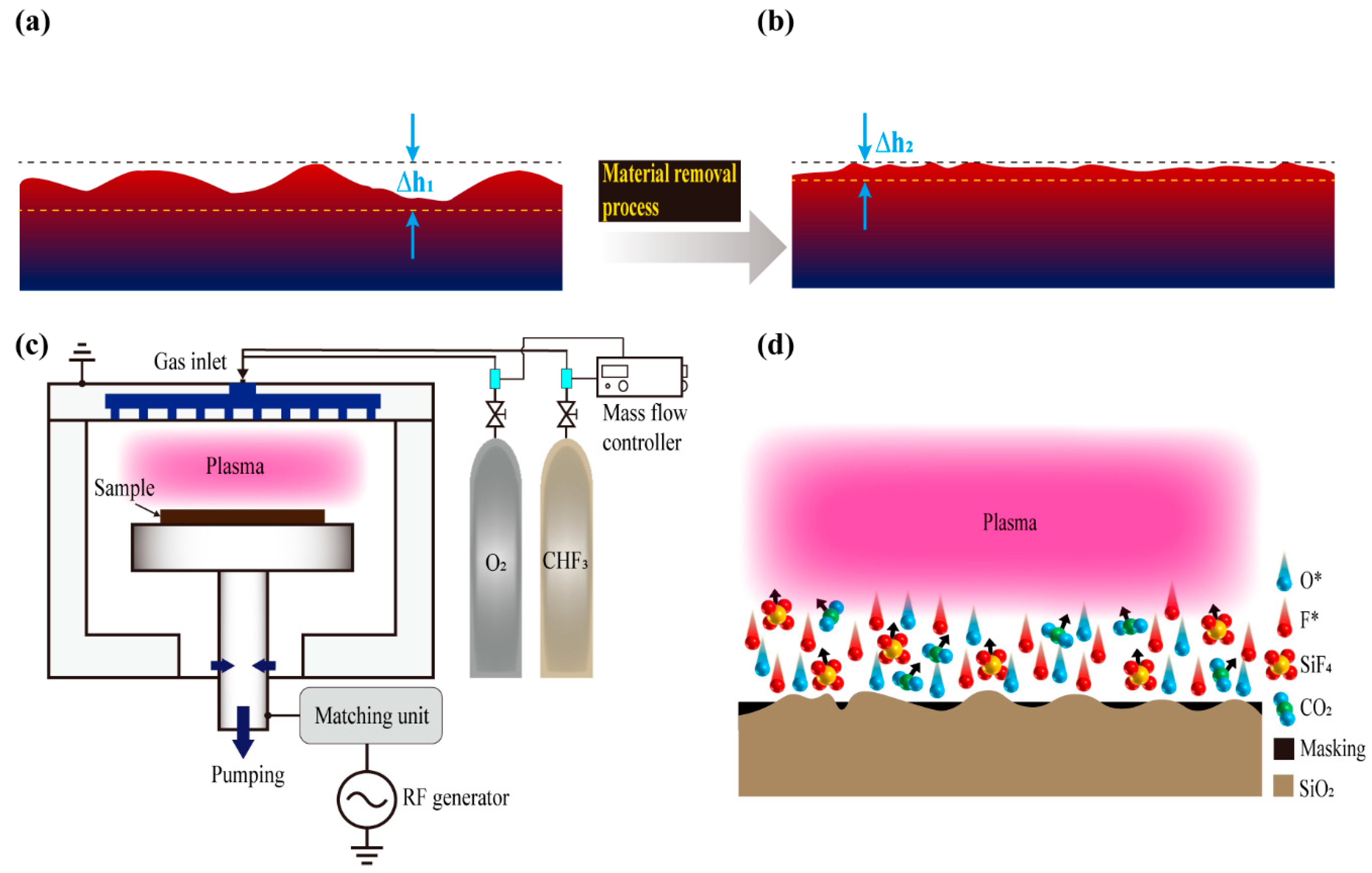
3. Experimental
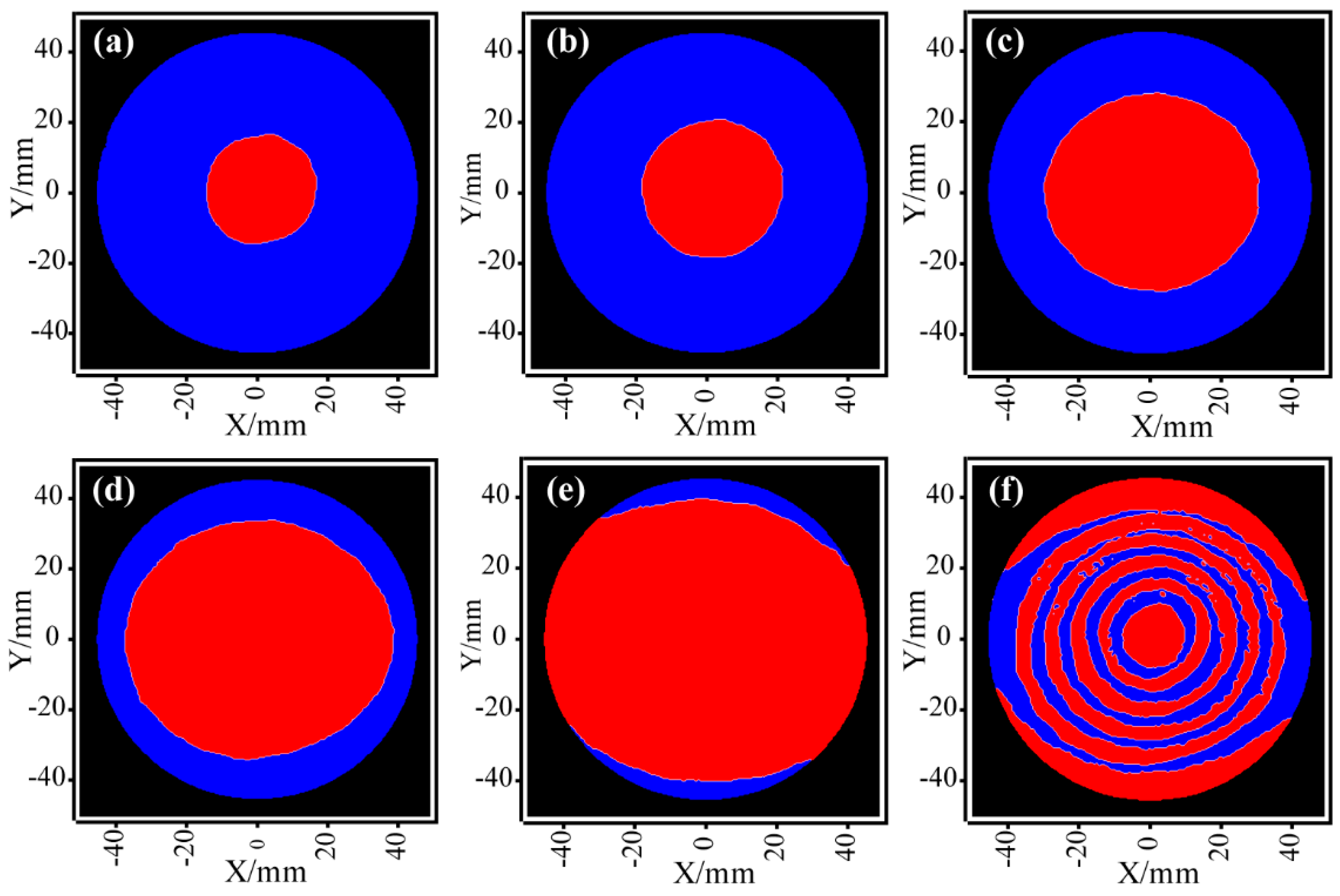
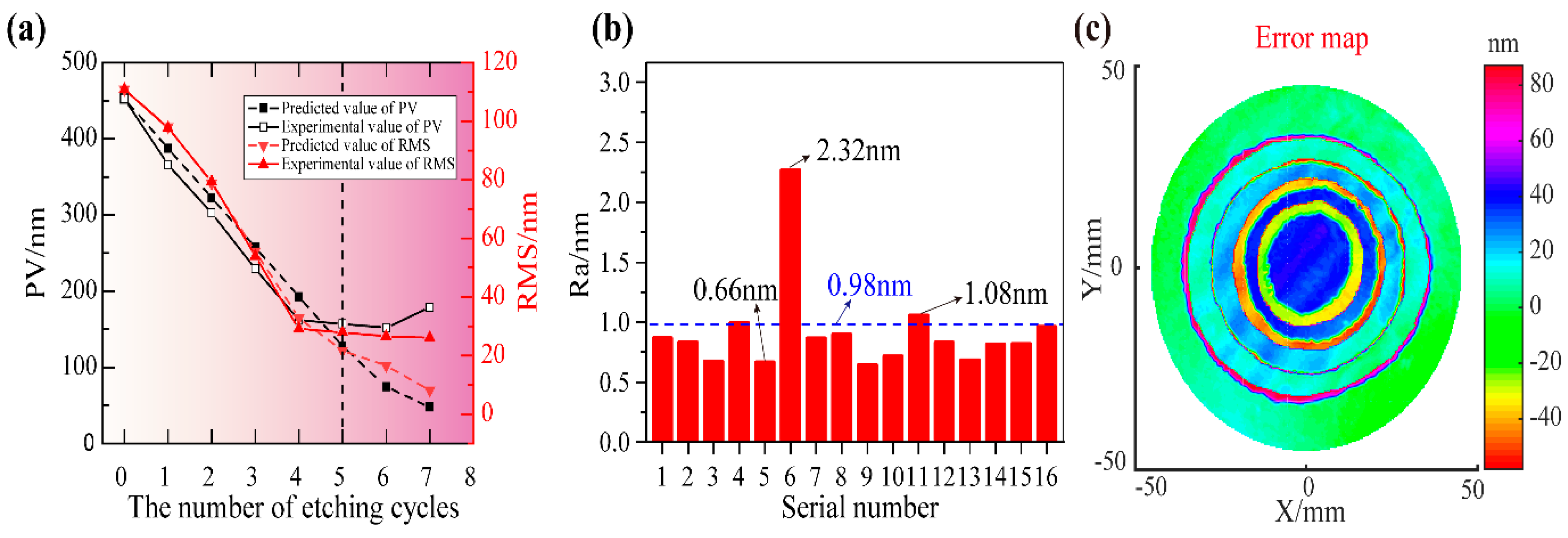
4. Results and Discussion
5. Conclusions
Author Contributions
Funding
Data Availability Statement
Conflicts of Interest
References
- Su, X.; Ji, P.; Jin, Y.; Li, D.; Walker, D.; Yu, G.; Li, H.; Wang, B. Simulation and experimental study on form-preserving capability of bonnet polishing for complex freeform surfaces. Precis. Eng. 2019, 60, 54–62. [Google Scholar] [CrossRef]
- Jin, M.S.; Ji, S.M.; Zhang, L.; Zhang, X.; Shen, Y.Q. Effect of Free Abrasive Particle in Gasbag Polishing Technique. Adv. Mater. Res. 2009, 69, 83–87. [Google Scholar] [CrossRef]
- Cao, Z.-C.; Cheung, C.F. Multi-scale modeling and simulation of material removal characteristics in computer-controlled bonnet polishing. Int. J. Mech. Sci. 2016, 106, 147–156. [Google Scholar] [CrossRef]
- Guo, Y.; Yin, S.; Ohmori, H.; Li, M.; Chen, F.; Huang, S. A novel high efficiency magnetorheological polishing process excited by Halbach array magnetic field. Precis. Eng. 2022, 74, 175–185. [Google Scholar] [CrossRef]
- Mi, S.; Toros, A.; Graziosi, T.; Quack, N. Non-contact polishing of single crystal diamond by ion beam etching. Diam. Relat. Mater. 2019, 92, 248–252. [Google Scholar] [CrossRef]
- Zhao, L.; Cheng, J.; Chen, M.; Yuan, X.; Liao, W.; Liu, Q.; Yang, H.; Wang, H. Formation mechanism of a smooth, defect-free surface of fused-silica optics using rapid CO2 laser polishing. Int. J. Extrem. Manuf. 2019, 1, 035001. [Google Scholar] [CrossRef]
- Tan, C.; Zhao, L.; Chen, M.; Cheng, J.; Yang, H.; Liu, Q.; Yin, Z.; Liao, W. Formation mechanism of surface morphology in the process of CO2 pulsed laser processing of fused silica optics. Opt. Laser Eng. 2021, 138, 106838. [Google Scholar] [CrossRef]
- Tian, F.; Li, Z.; Lv, C.; Liu, G. Polishing pressure investigations of robot automatic polishing on curved surfaces. Int. J. Adv. Manuf. Technol. 2016, 87, 639–646. [Google Scholar] [CrossRef]
- Wu, J.; Zhang, P.; Yu, D.; Zhang, S.; Xin, Q.; Wan, Y. Monitoring and diagnosis of the inductively coupled atmospheric pressure plasma jet for deterministic optical processing. Optik 2020, 214, 164815. [Google Scholar] [CrossRef]
- Jones, R.A. Optimization of computer controlled polishing. Appl. Opt. 1977, 16, 218–224. [Google Scholar] [CrossRef]
- Dunn, C.R.; Walker, D.D. Pseudo-random tool paths for CNC sub-aperture polishing and other applications. Opt. Express 2008, 16, 18942–18949. [Google Scholar] [CrossRef] [PubMed]
- Dong, Z.; Nai, W. Surface ripple suppression in subaperture polishing with fragment-type tool paths. Appl. Opt. 2018, 57, 5523–5532. [Google Scholar] [CrossRef] [PubMed]
- Takizawa, K.; Beaucamp, A. Comparison of tool feed influence in CNC polishing between a novel circular-random path and other pseudo-random paths. Opt. Express 2017, 25, 22411–22424. [Google Scholar] [CrossRef] [PubMed]
- Lallement, L.; Rhallabi, A.; Cardinaud, C.; Fernandez, M.C.P. Modelling of fluorine based high density plasma for the etching of silica glasses. J. Vac. Sci. Technol. A 2011, 29, 0513041–0513049. [Google Scholar] [CrossRef]
- Hrubesh, L.W.; Norton, M.A.; Molander, W.A.; Donohue, E.E.; Maricle, S.M.; Penetrante, B.; Brusasco, R.M.; Grundler, W.; Butler, J.A.; Carr, J.; et al. Methods for mitigating surface damage growth in NIF final optics. Proc. SPIE 2002, 4679, 23–33. [Google Scholar] [CrossRef]
- Donnelly, V.M.; Kornblit, A. Plasma etching: Yesterday, today, and tomorrow. J. Vac. Sci. Technol. A 2013, 31, 050825. [Google Scholar] [CrossRef] [Green Version]
- Ventzek, P.; Rauf, S.; Stout, P.; Zhang, D.; Dauksher, W.; Hall, E. Application and simulation of low temperature plasma processes in semiconductor manufacturing. Appl. Surf. Sci. 2002, 192, 201–215. [Google Scholar] [CrossRef]
- Kawakami, R.; Tominaga, K.; Okada, K.; Nouda, T.; Inaoka, T.; Takeichi, A.; Fukudome, T.; Murao, K. Etch damage characteristics of TiO2 thin films by capacitively coupled RF Ar plasmas. Vacuum 2010, 84, 1393–1397. [Google Scholar] [CrossRef]
- Leopold, S.; Krenin; Ulbrich, A.; Krischock, S.; Hoffman, M. Formation of silicon grass: Nanomasking by carbon clusters in cyclic deep reactive ion etching. J. Vac. Sci. Technol. B 2011, 29, 011002. [Google Scholar] [CrossRef]
- Hotovy, I.; Hascik, S.; Gregor, M.; Rehacek, V.; Predanocy, M.; Plecenik, A. Dry etching characteristics of TiO2 thin films using inductively coupled plasma for gas sensing. Vacuum 2014, 107, 20–22. [Google Scholar] [CrossRef]
- Sanghoo, P.; Wonho, C.; Holak, K. Electron heating in rf capacitive discharges at atmospheric-to-subatmospheric pressures. Sci. Rep. 2018, 8, 10217. [Google Scholar]
- Liu, D.W.; Iza, F.; Kong, M.G. Electron heating in radio-frequency capacitively coupled atmospheric-pressure plasmas. Appl. Phys. Lett. 2008, 93, 261503. [Google Scholar] [CrossRef] [Green Version]
- Kim, H.J.; Kim, J.S.; Lee, H.J. Numerical analysis for optimization of the sidewall conditions in a capacitively coupled plasma deposition reactor. J. Appl. Phys. 2019, 126, 173301. [Google Scholar] [CrossRef]
- Zhang, Q.-Z.; Zhao, S.-X.; Jiang, W.; Wang, Y.-N. Separate control between geometrical and electrical asymmetry effects in capacitively coupled plasmas. J. Phys. D Appl. Phys. 2012, 45, 305203. [Google Scholar] [CrossRef]
- Li, Z.; Shao, J.; Luo, Q.; Lei, B.; Gao, G.; Bian, J.; Wu, S.; Fan, B. Highly accurate positioned, rapid figure correction by reactive ion etching for large aperture lightweight membrane optical elements. OSA Contin. 2019, 2, 3350–3357. [Google Scholar] [CrossRef]
- Wu, X.; Fan, B.; Xin, Q.; Gao, G.; Jiao, P.; Shao, J.; Luo, Q.; Liang, Z. The Tailored Material Removal Distribution on Polyimide Membrane Can Be Obtained by Introducing Additional Electrodes. Polymers 2023, 15, 2394. [Google Scholar] [CrossRef]
- Sun, R.; Yang, X.; Watanabe, K.; Miyazaki, S.; Fukano, T.; Kitada, M.; Arima, K.; Kawai, K.; Yamamura, K. Etching Characteristics of Quartz Crystal Wafers Using Argon-Based Atmospheric Pressure CF4 Plasma Stabilized by Ethanol Addition. Nanomanufacturing Metrol. 2019, 2, 168–176. [Google Scholar] [CrossRef]
- Dong, Z.; Cheng, H.; Tam, H.-Y. Modified dwell time optimization model and its applications in subaperture polishing. Appl. Opt. 2014, 53, 3213–3224. [Google Scholar] [CrossRef]
- Wang, C.; Yang, W.; Wang, Z.; Yang, X.; Hu, C.; Zhong, B.; Guo, Y.; Xu, Q. Dwell-time algorithm for polishing large optics. Appl. Opt. 2014, 53, 4752–4760. [Google Scholar] [CrossRef]
- Luo, Q.; Li, Z.; Wu, X.; Shao, J.; Fan, B.; Wu, S.; Du, J. Figure correction of a quartz sub-mirror for a transmissive diffractive segmented telescope by Reactive Ion Figuring. IEEE Photon-Technol. Lett. 2022, 34, 1143–1146. [Google Scholar] [CrossRef]
- Li, D.; Li, N.; Su, X.; Liu, K.; Ji, P.; Wang, B. Characterization of fused silica surface topography in capacitively coupled at-mospheric pressure plasma processing. Appl. Surf. Sci. 2019, 489, 648–657. [Google Scholar] [CrossRef]
- Gong, C.; Fan, B.; Shao, J.; Liu, X. High precision fabrication method of diffractive lens on large aperture quartz substrate. Acta Photonica Sin. 2020, 49, 0522001. [Google Scholar] [CrossRef]


| ReactionGas | CHF3, O2; the gas flow rate is 50 sccm and 95 sccm, respectively |
| Chamber pressure | 1.5 Pa |
| Distance between electrodes | 75 mm |
| Masking layer material | UV-curable ink |
| Workpieces | Plat mirror with 101.6 mm aperture |
| Workpiece material | SiO2 |
| Radio frequency power | 800 W |
| Driving frequency | 13.56 MHz |
Disclaimer/Publisher’s Note: The statements, opinions and data contained in all publications are solely those of the individual author(s) and contributor(s) and not of MDPI and/or the editor(s). MDPI and/or the editor(s) disclaim responsibility for any injury to people or property resulting from any ideas, methods, instructions or products referred to in the content. |
© 2023 by the authors. Licensee MDPI, Basel, Switzerland. This article is an open access article distributed under the terms and conditions of the Creative Commons Attribution (CC BY) license (https://creativecommons.org/licenses/by/4.0/).
Share and Cite
Wu, X.; Fan, B.; Xin, Q.; Luo, Q.; Shao, J.; Gao, G.; Jiao, P. Plasma Figure Correction Method Based on Multiple Distributed Material Removal Functions. Micromachines 2023, 14, 1193. https://doi.org/10.3390/mi14061193
Wu X, Fan B, Xin Q, Luo Q, Shao J, Gao G, Jiao P. Plasma Figure Correction Method Based on Multiple Distributed Material Removal Functions. Micromachines. 2023; 14(6):1193. https://doi.org/10.3390/mi14061193
Chicago/Turabian StyleWu, Xiang, Bin Fan, Qiang Xin, Qian Luo, Junming Shao, Guohan Gao, and Peiqi Jiao. 2023. "Plasma Figure Correction Method Based on Multiple Distributed Material Removal Functions" Micromachines 14, no. 6: 1193. https://doi.org/10.3390/mi14061193