

An 8–18 GHz 90° Switched T-Type Phase Shifter
 , , and
Abstract
:1. Introduction
2. Circuit Design
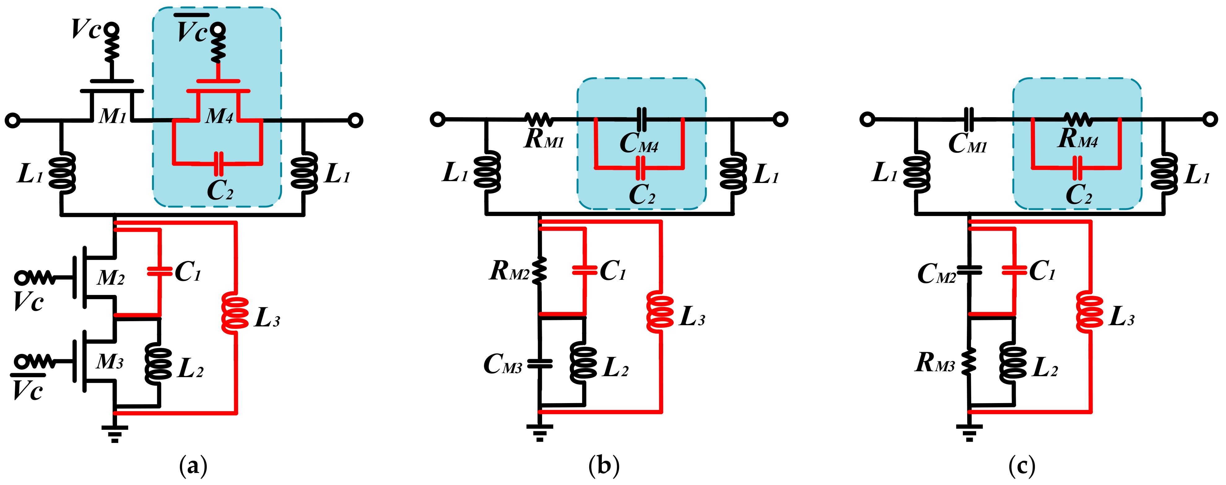
2.1. Typical Switched Phase Shifting Cells
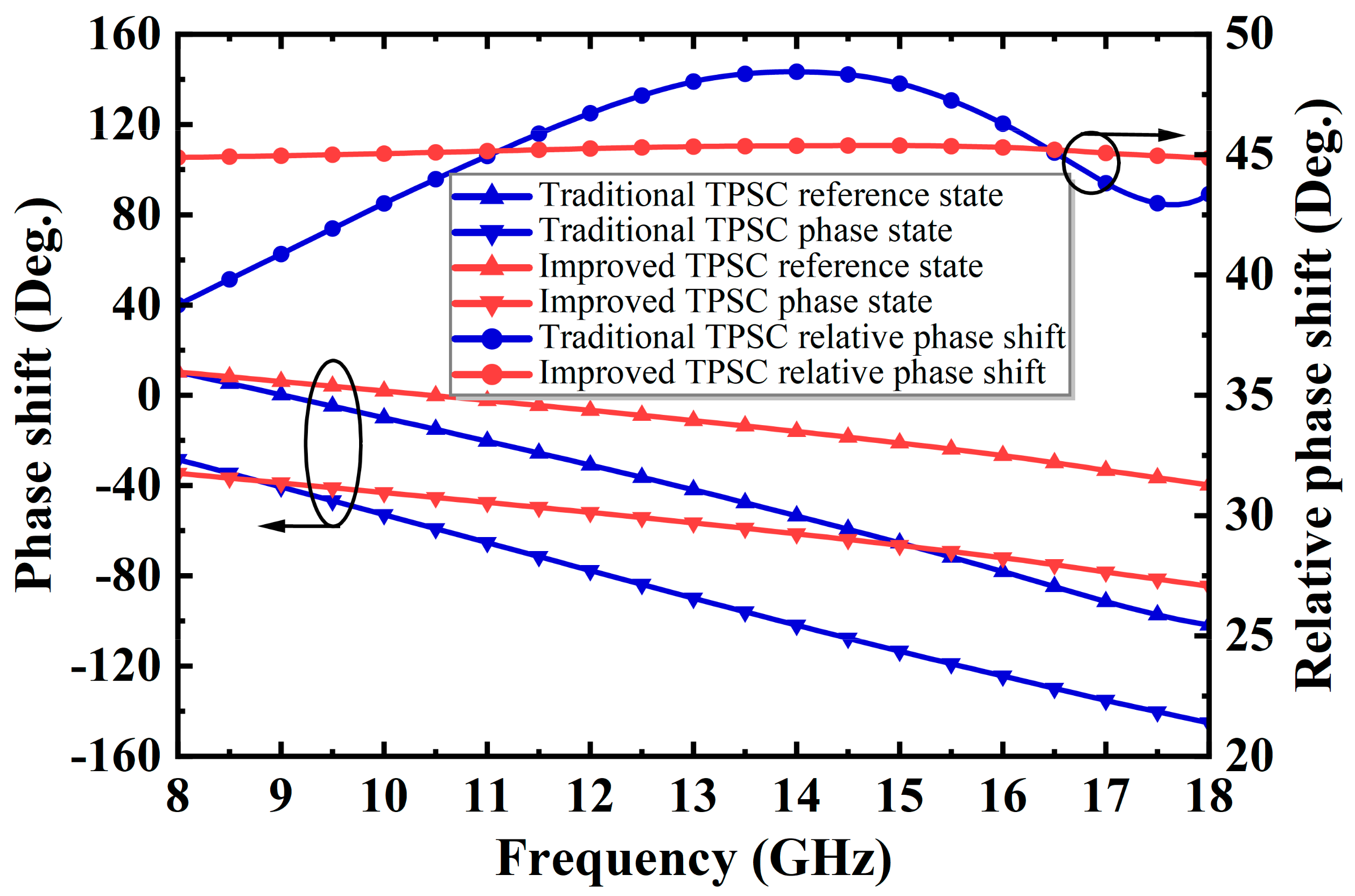
2.2. Conventional TPSCs
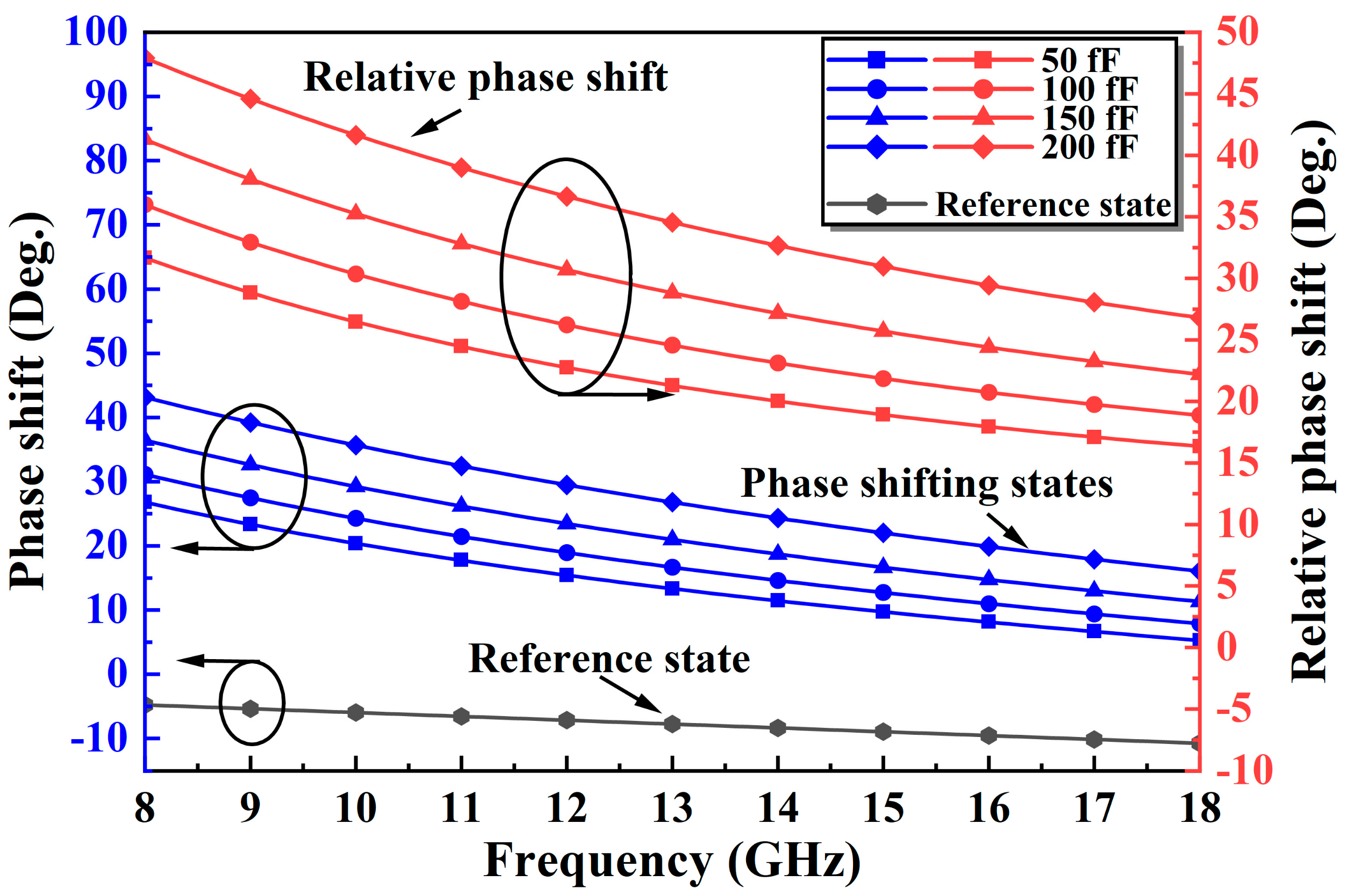
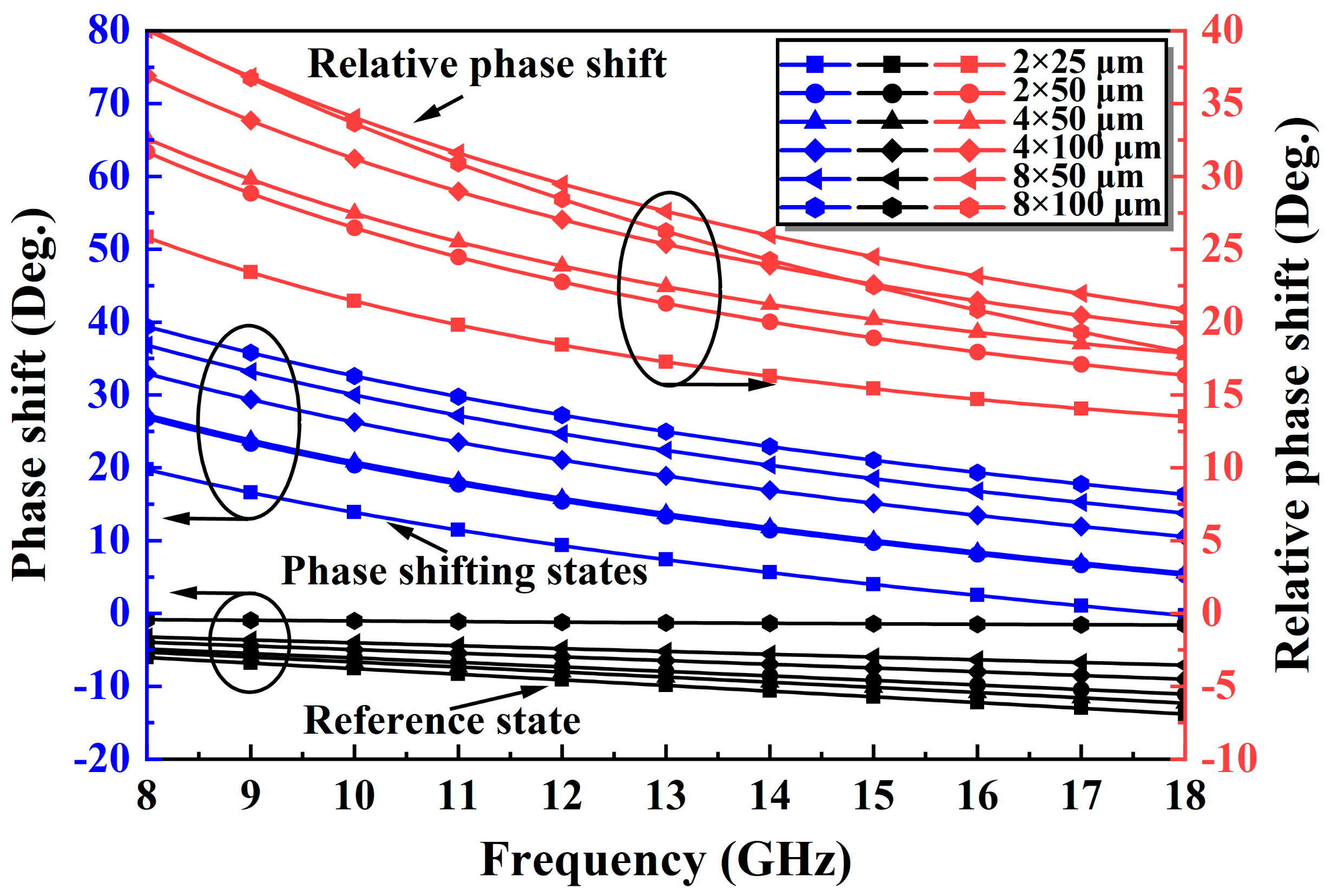
2.3. Improved TPSCs
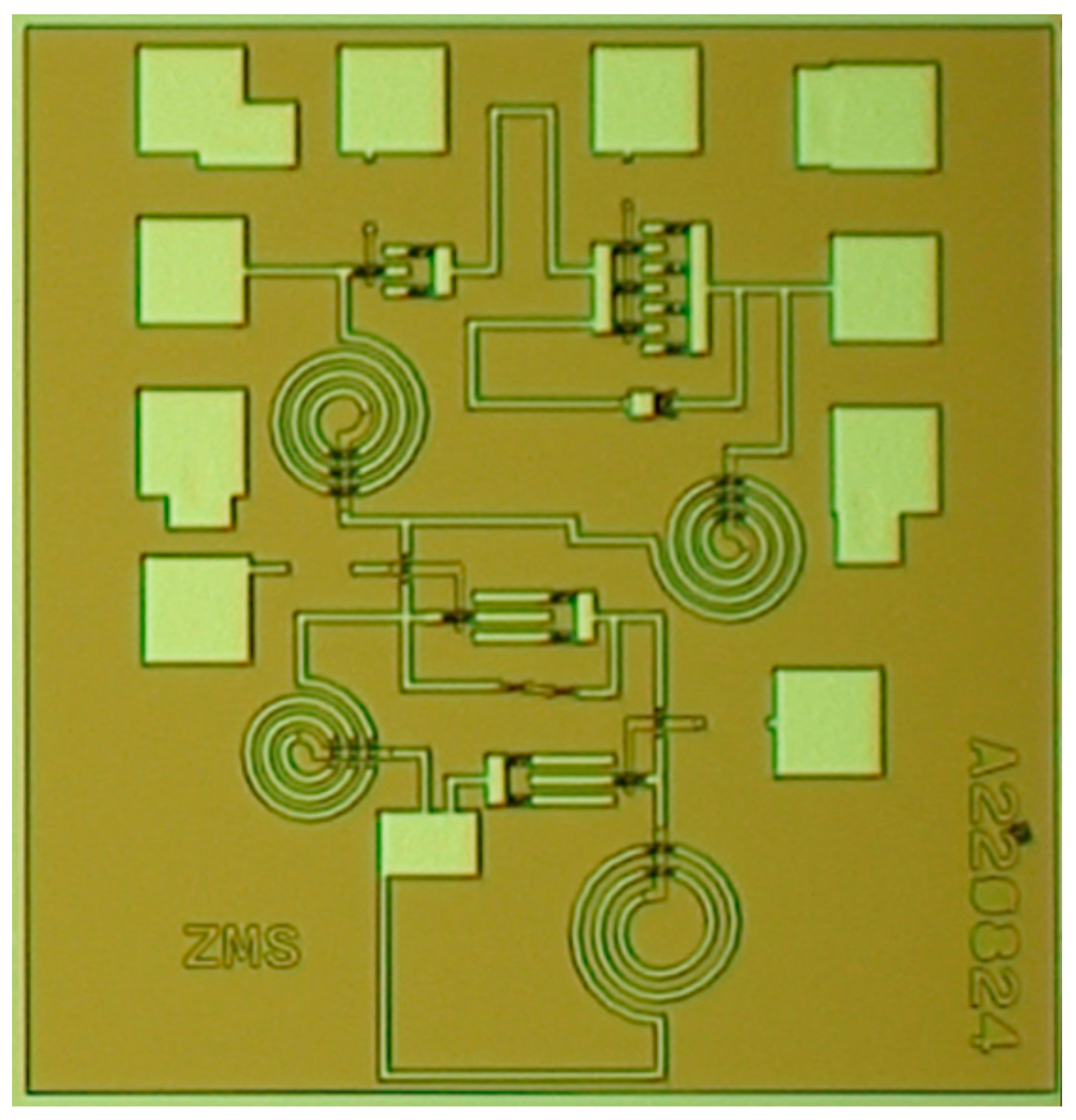
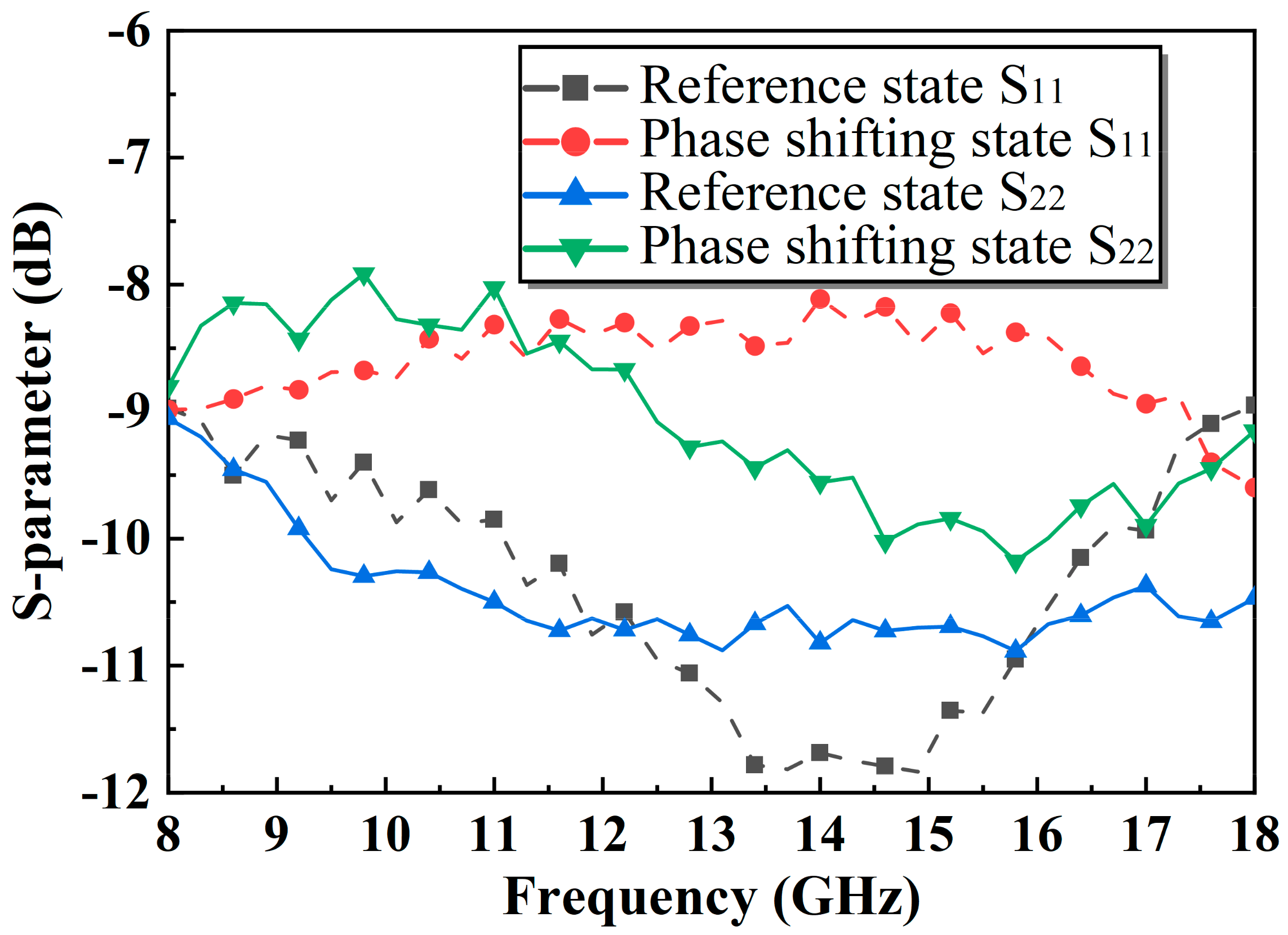
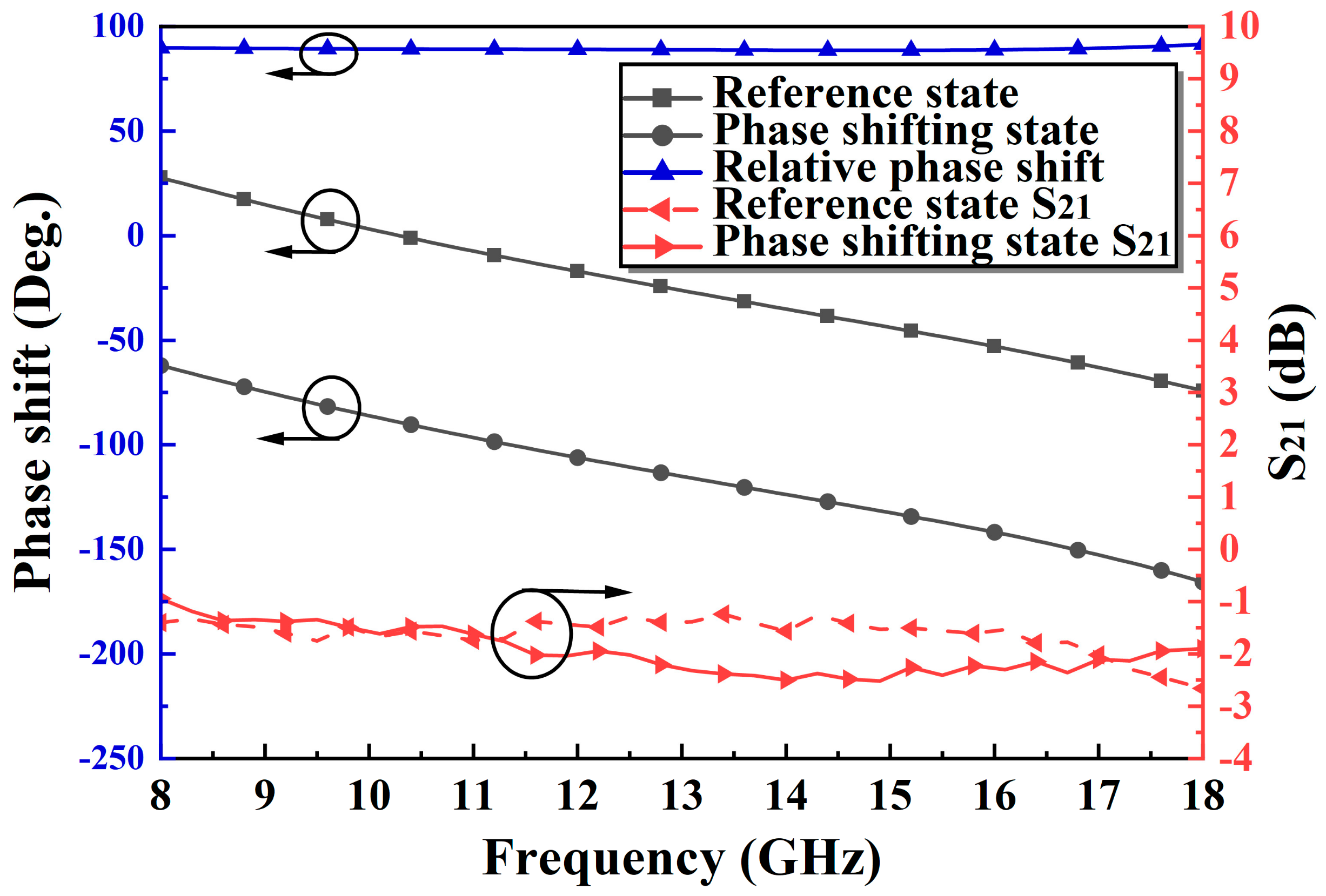
3. Measured Results
4. Conclusions
Author Contributions
Funding
Data Availability Statement
Conflicts of Interest
References
- Bahl, I.J.; Conway, D. L- and S-Band Compact Octave Bandwidth 4-bit MMIC Phase Shifters. IEEE Trans. Microw. Theory Tech. 2008, 56, 293–299. [Google Scholar] [CrossRef]
- An, J.; Wang, G.-M.; Zhang, C.-X.; Qu, S.-B.; Zhang, P. Broadband digital phase shifter based on composite right/left-handed transmission line. Microw. Opt. Technol. Lett. 2008, 50, 2365–2368. [Google Scholar] [CrossRef]
- Zeng, J.; Xie, C.; Zhang, D.; Feng, J.; Tan, C.; Yu, Z. A wideband accurate compact 6-bit phase shifter in 0.15-μm GaAs technology. Microw. Opt. Technol. Lett. 2023, 65, 534–540. [Google Scholar] [CrossRef]
- Chen, J.; Mou, S.; Ma, K.; Meng, F. A 3–6-GHz Wideband Compact 6-Bit Phase Shifter in 0.5-μm GaAs Technology. IEEE Microw. Wirel. Compon. Lett. 2020, 30, 794–797. [Google Scholar] [CrossRef]
- Li, X.; Fu, H.; Ma, K.; Hu, J. A 2.4–4-GHz Wideband 7-Bit Phase Shifter with Low RMS Phase/Amplitude Error in 0.5-μm GaAs Technology. IEEE Trans. Microw. Theory Tech. 2022, 70, 1292–1301. [Google Scholar] [CrossRef]
- Kang, D.W.; Lee, H.D.; Kim, C.H.; Hong, S. Ku-band MMIC phase shifter using a parallel resonator with 0.18-μm CMOS technology. IEEE Trans. Microw. Theory Tech. 2006, 54, 294–301. [Google Scholar] [CrossRef]
- Song, I.S.; Yoon, G.; Park, C.S. A Highly Integrated 1-Bit Phase Shifter Based on High-Pass/Low-Pass Structure. IEEE Microw. Wirel. Compon. Lett. 2015, 25, 523–525. [Google Scholar] [CrossRef]
- Biglarbegian, B.; Nezhad-Ahmadi, M.R.; Fakharzadeh, M.; Safavi-Naeini, S. Millimeter-Wave Reflective-Type Phase Shifter in CMOS Technology. IEEE Microw. Wirel. Compon. Lett. 2009, 19, 560–562. [Google Scholar] [CrossRef]
- Lyu, Y.P.; Zhu, L.; Cheng, C.H. A New Design of Ultrawideband Single-Layer 90° Phase Shifter in the View of Group Delay. IEEE Microw. Wirel. Compon. Lett. 2019, 29, 376–378. [Google Scholar] [CrossRef]
- Honari, M.M.; Mirzavand, R.; Mousavi, P. Wideband and Ultrawideband Phase Shifter Designs Based on Low-Pass/Bandpass/High-Pass Networks. IEEE Trans. Compon. Packag. Manuf. Technol. 2018, 8, 1056–1065. [Google Scholar] [CrossRef]
- Zhang, W.; Xu, K.; Shi, J.; Shen, Z. A Compact Single-Layer Balanced Phase Shifter with Wide Bandwidth and Uniform Reference Line. IEEE Access 2020, 8, 41530–41536. [Google Scholar] [CrossRef]
- Dong, Q.; Wu, Y.; Zheng, Y.; Wang, W.; Liu, Y. A Compact Single-Layer Ultra-Wideband Phase Shifter Using Weakly Coupled Lines. IEEE Access 2019, 7, 12575–12583. [Google Scholar] [CrossRef]
- Jeon, H.; Kobayashi, K.W. A High Linearity +44.5-dBm IP3 C-Band 6-Bit Digital Phase Shifter Using SOI Technology for Phased Array Applications. IEEE Microw. Wirel. Compon. Lett. 2019, 29, 733–736. [Google Scholar] [CrossRef]
- Hangai, M.; Hieda, M.; Yunoue, N.; Sasaki, Y.; Miyazaki, M. S- and C-Band Ultra-Compact Phase Shifters Based on All-Pass Networks. IEEE Trans. Microw. Theory Tech. 2010, 58, 41–47. [Google Scholar] [CrossRef]
- Meghdadi, M.; Azizi, M.; Kiani, M.; Medi, A.; Atarodi, M. A 6-Bit CMOS Phase Shifter for S-Band. IEEE Trans. Microw. Theory Tech. 2010, 58, 3519–3526. [Google Scholar] [CrossRef]


| Reference | BW (GHz) | BW (%) | Phase Shift (°) | Error (°) | (dB) | IL (dB) | Process |
|---|---|---|---|---|---|---|---|
| [7] MWCL’2015 | 57–63 | 10 | 90 | ±3 | <−10, <−10 | <5.2 | 65 nm CMOS |
| [8] MWCL’2009 | 50–65 | 26 | 90 | ±1 | <−11, <−11 | <8 | 90 nm CMOS |
| [13] MWCL’2019 | 5–6 | 18.2 | 90 | ±2 | <−11, <−11 | <4 * | 0.18 μm CMOS |
| [14] TMTT’2010 | S/C | 10 | 90 | ±3 | <−10, <−10 | <7 * | 0.5 μm pHEMT |
| [15] TMTT’2010 | 2.5–3.2 | 25 | 90 | ±2 | <−8, <−9 | <3 * | 0.18 μm CMOS |
| [4] MWCL’2020 | 3–6 | 66.7 | 90 | ±2 | <−8, <−8 | <6 | 0.5 μm pHEMT |
| This work | 8–18 | 77 | 90 | ±1.5 | <−8, <−8 | <2.6 | 0.15 μm pHEMT |
Disclaimer/Publisher’s Note: The statements, opinions and data contained in all publications are solely those of the individual author(s) and contributor(s) and not of MDPI and/or the editor(s). MDPI and/or the editor(s) disclaim responsibility for any injury to people or property resulting from any ideas, methods, instructions or products referred to in the content. |
© 2023 by the authors. Licensee MDPI, Basel, Switzerland. This article is an open access article distributed under the terms and conditions of the Creative Commons Attribution (CC BY) license (https://creativecommons.org/licenses/by/4.0/).
Share and Cite
Zeng, J.; Ren, Y.; Tan, C.; Yuan, Y.; Li, J.; Yu, Z. An 8–18 GHz 90° Switched T-Type Phase Shifter. Micromachines 2023, 14, 1569. https://doi.org/10.3390/mi14081569
Zeng J, Ren Y, Tan C, Yuan Y, Li J, Yu Z. An 8–18 GHz 90° Switched T-Type Phase Shifter. Micromachines. 2023; 14(8):1569. https://doi.org/10.3390/mi14081569
Chicago/Turabian StyleZeng, Jialong, Yuxin Ren, Cheng Tan, Yang Yuan, Jiaxuan Li, and Zhongjun Yu. 2023. "An 8–18 GHz 90° Switched T-Type Phase Shifter" Micromachines 14, no. 8: 1569. https://doi.org/10.3390/mi14081569