
Optoelectronic Effects of Copper–Indium–Gallium–Sulfur (CIGS2)-Solar Cells Prepared by Three-Stage Co-Evaporation Process Technology

 ,
,
Abstract
:1. Introduction
2. Experiments and Measurements
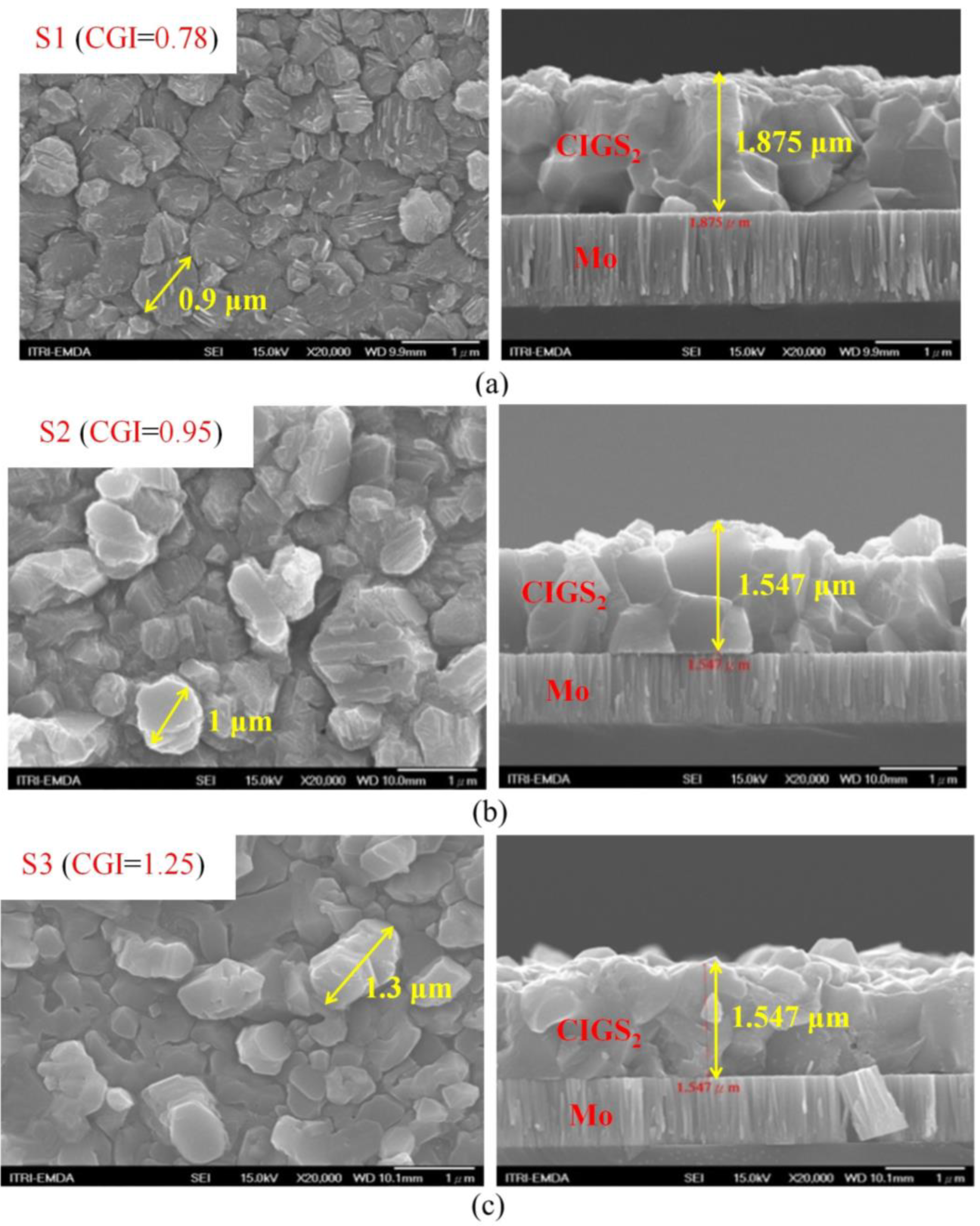
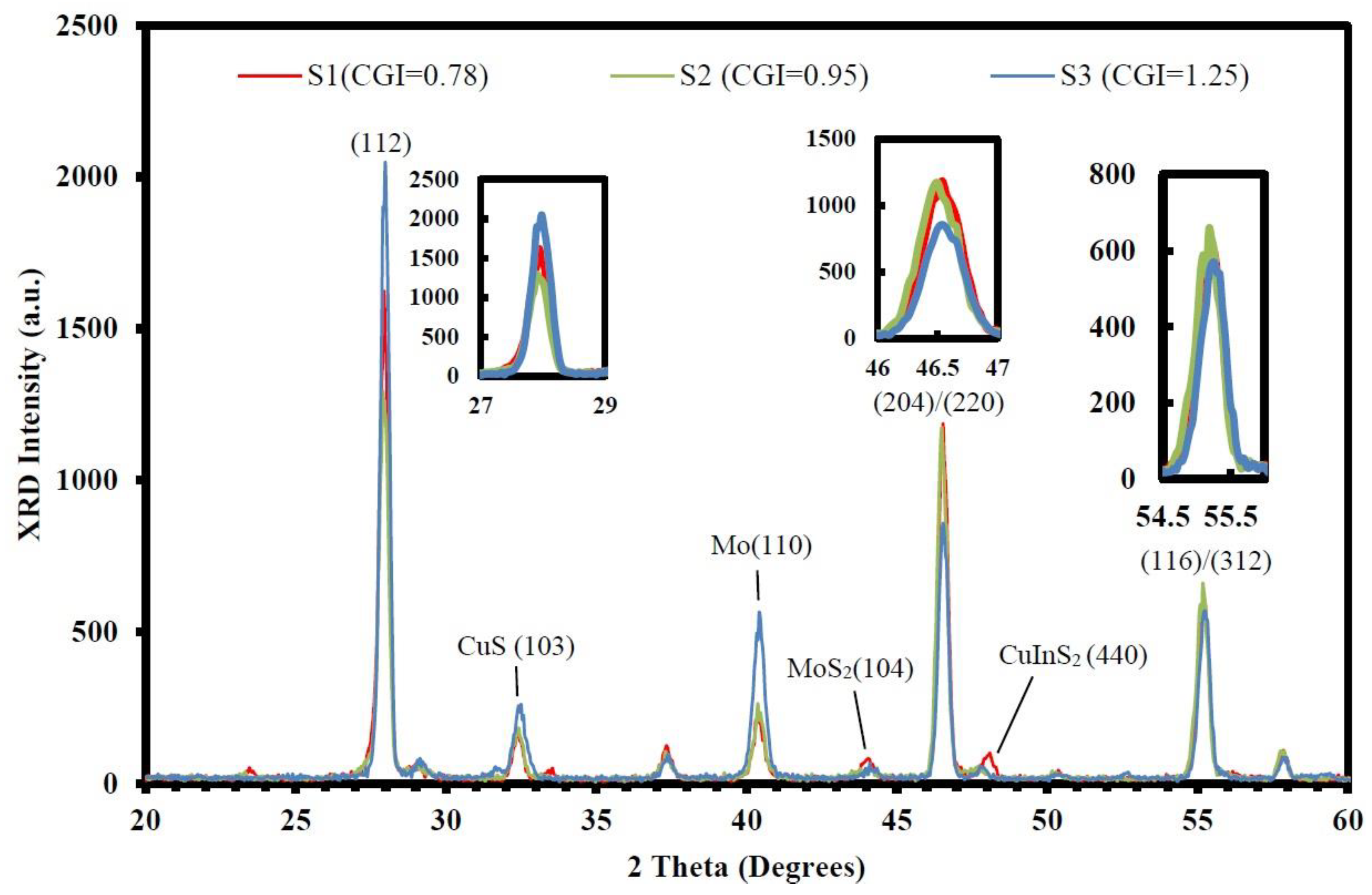
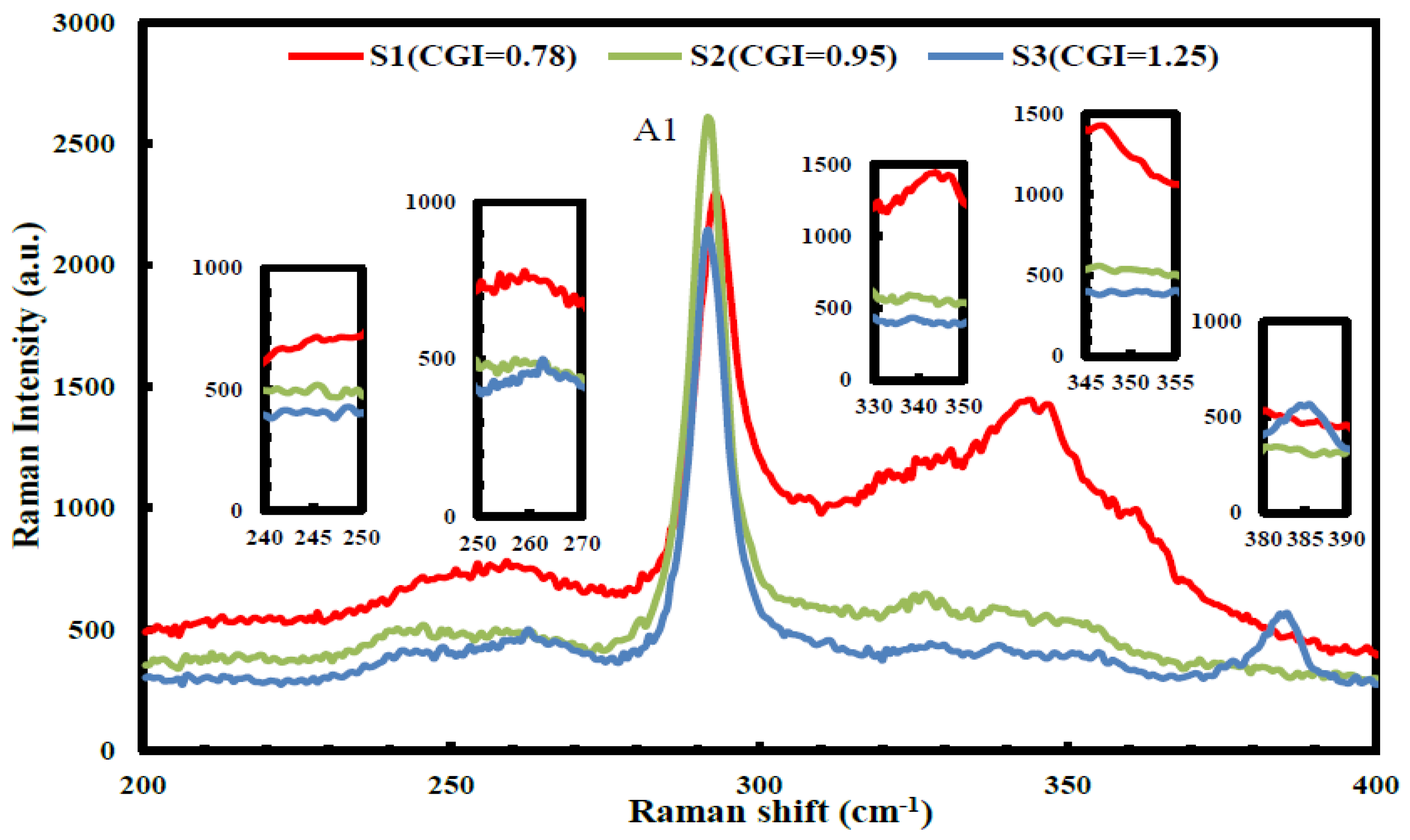
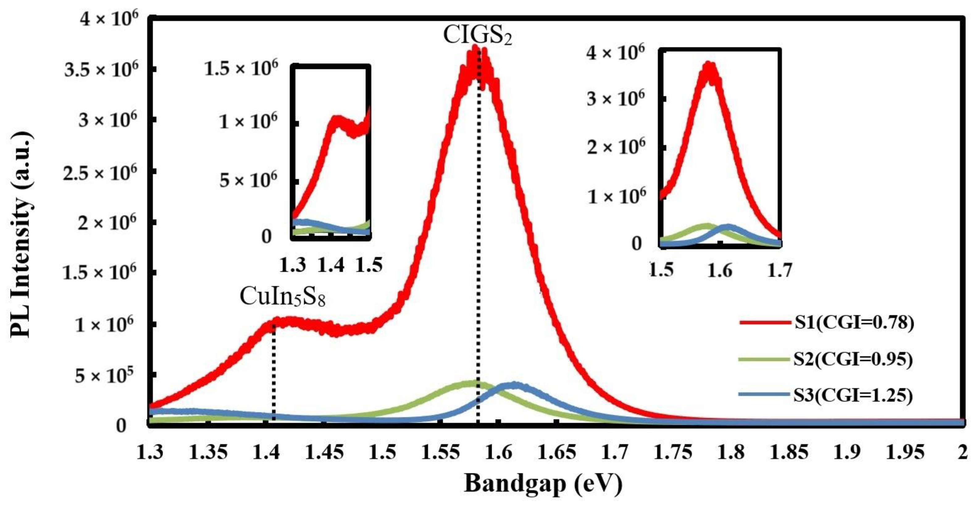
3. Results and Discussion
4. Conclusions
Author Contributions
Funding
Data Availability Statement
Conflicts of Interest
References
- International Energy Agency. Renewables 2019, Market Analysis and Forecast from 2019 to 2024; IEA: Paris, France, 2019; Available online: https://www.iea.org/reports/renewables-2019 (accessed on 10 February 2023).
- Alanazi, T.I.; Sabbagh, M.E. Proposal and Design of Flexible All-Polymer/CIGS Tandem Solar Cell. Polymers 2023, 15, 1823. [Google Scholar] [CrossRef]
- Nafie, N.; Abouda Lachiheb, M.; Ben Rabha, M.; Dimassi, W.; Bouaïcha, M. Effect of the doping concentration on the properties of silicon nanowires. Phys. E Low Dimens. Syst. Nanostruct. 2014, 56, 427–430. [Google Scholar] [CrossRef]
- Karyaoui, M.; Bardaoui, A.; Rabha, M.B.; Harmand, J.C.; Amlouk, M. Effect of rapid oxidation on optical and electrical properties of silicon nanowires obtained by chemical etching. Eur. Phys. J. Appl. Phys. 2012, 58, 20103. [Google Scholar] [CrossRef]
- Bourlier, Y.; Cristini Robbe, O.; Lethien, C.; Roussel, P.; Pastre, A.; Zegaoui, M.; Bernard, R. Control of gallium incorporation in sol–gel derived CuIn(1−x)GaxS2 thin films for photovoltaic applications. Mater. Res. Bull. 2015, 70, 137–144. [Google Scholar] [CrossRef]
- Ho, J.-S.; Chang, S.-C.; Ho, J.-J.; Hsu, W.-T.; Chiang, C.-C.; Tsai, S.-Y.; Wang, S.-S.; Lin, C.-K.; Chou, C.-C.; Yeh, C.-H.; et al. Improving the Performance of Solar Cells with Novel Buffer Structure by the Chemical Bath Deposition Technique. Mater. Sci. Semicond. Process. 2017, 59, 29–34. [Google Scholar] [CrossRef]
- Ahmad, F.; Anderson, T.H.; Monk, P.B.; Lakhtakia, A. Efficiency enhancement of ultrathin CIGS solar cells by optimal bandgap grading. Appl. Opt. 2019, 58, 6067–6078. [Google Scholar] [CrossRef]
- Nakamura, M.; Yamaguchi, K.; Kimoto, Y.; Yasaki, Y.; Kato, T.; Sugimoto, H. Cd-Free Cu(In,Ga)(Se,S)2 Thin-Film Solar Cell with Record Efficiency of 23.35%. IEEE J. Photovolt. 2019, 9, 1863–1867. [Google Scholar] [CrossRef]
- Santos, P.; Brito, D.; Anacleto, P.; Fonseca, J.; de Brito Sousa, D.; Tavares, C.J.; Virtuoso, J.; Alves, M.; Pérez-Rodríguez, A.; Sadewasser, S. Effect of Cu-In-Ga Target Composition on Hybrid-Sputtered Cu(In,Ga)Se2 Solar Cells. IEEE J. Photovolt. 2021, 11, 1206–1212. [Google Scholar] [CrossRef]
- Rudmann, D.; Brémaud, D.; da Cunha, A.F.; Bilger, G.; Strohm, A.; Kaelin, M.; Zogg, H.; Tiwari, A.N. Sodium incorporation strategies for CIGS growth at different temperatures. Thin Solid Films 2005, 480–481, 55–60. [Google Scholar] [CrossRef]
- Li, W.; Yao, L.; Li, K.; Li, X.; Yang, B.; Xu, S.; Shi, S.; Yi, C.; Chen, M.; Feng, Y.; et al. Enabling Low-Temperature Deposition of High-Efficiency CIGS Solar Cells with a Modified Three-Stage Co-Evaporation Process. ACS Appl. Energy Mater. 2020, 3, 4201–4207. [Google Scholar] [CrossRef]
- Álvarez-García, J.; Pérez-Rodríguez, A.; Romano-Rodríguez, A.; Calvo-Barrio, L.; Barcones, B.; Morante, J.R.; Siemer, K.; Luck, I.; Klenk, R. Microstructural characterisation of CuInS2 polycrystalline films sulfurised by rapid thermal processing. Thin Solid Films 2001, 387, 219–221. [Google Scholar] [CrossRef]
- Merdes, S.; Mainz, R.; Klaer, J.; Meeder, A.; Rodriguez-Alvarez, H.; Schock, H.W.; Klenk, R. 12.6% efficient CdS/Cu (In, Ga) S2-based solar cell with an open circuit voltage of 879 mV prepared by a rapid thermal process. Sol. Energy Mater. Sol. Cells 2011, 95, 864–869. [Google Scholar] [CrossRef]
- Hanna, G.; Jasenek, A.; Rau, U.; Schock, H.W. Influence of the Ga-content on the bulk defect densities of Cu(In,Ga)Se2. Thin Solid Films 2001, 387, 71–73. [Google Scholar] [CrossRef]
- Singh, S.; Samji, S.K.; Ramachandra Rao, M.S. Synthesis and characterisation of CuInGaS2 nano-ink for photovoltaic applications. J. Exp. Nanosci. 2013, 8, 320–325. [Google Scholar] [CrossRef]
- Gao, Q.; Yuan, S.; Zhou, Z.; Kou, D.; Zhou, W.; Meng, Y.; Qi, Y.; Han, L.; Wu, S. Over 16% Efficient Solution-Processed Cu(In,Ga)Se2 Solar Cells via Incorporation of Copper-Rich Precursor Film. Small Adv. Sci. News 2022, 18, 2203443. [Google Scholar] [CrossRef]
- Ben Rabha, M.; Belhadj Mohamed, S.; Dimassi, W.; Gaidi, M.; Ezzaouia, H.; Bessaïs, B. Reduction of absorption loss in multicrystalline silicon via combination of mechanical grooving and porous silicon. Phys. Status Solidi C Curr. Top. Solid State Phys. 2011, 8, 883–886. [Google Scholar] [CrossRef]
- Wu, K.; Wang, D. Temperature-dependent Raman investigation of CuInS2 with mixed phases of chalcopyrite and CuAu. Phys. Status Solidi A 2011, 208, 2730–2736. [Google Scholar] [CrossRef]
- Nasser, S.; Alsloum, M.N.; Hussain, N. Preparing of Copper Oxides Thin Films by Chemical Bath Deposition (CBD) for Using in Environmental Application. Energy Procedia 2015, 74, 1459–1465. [Google Scholar] [CrossRef]
- Shukla, S.; Sood, M.; Adeleye, D.; Peedle, S.; Kusch, G.; Dahliah, D.; Melchiorre, M.; Rignanese, G.-M.; Hautier, G.; Oliver, R.; et al. Over 15% efficient wide-band-gap Cu(In,Ga)S2 solar cell: Suppressing bulk and interface recombination through composition engineering. Joule 2021, 5, 1816–1831. [Google Scholar] [CrossRef]
- Ho, J.; Wu, T.-C.; Ho, J.-J.; Hung, C.-H.; Chen, S.-Y.; Ho, J.-S.; Tsai, S.-Y.; Chou, C.-C.; Yeh, C.-H. Rear-Surface Line-Contact Optimization Using Screen-Print Techniques on Crystalline Solar Cells for Industrial Applications. Mater. Sci. Semicond. Process. 2018, 83, 22–26. [Google Scholar] [CrossRef]
- Chikate, B.V.; Sadawarte, Y.A. The Factors Affecting the Performance of Solar Cell. Int. J. Comput. Appl. 2015, 1, 1–5. [Google Scholar]
- Li, Z.; Yang, J.; Dezfuli, P.A.N. Study on the Influence of Light Intensity on the Performance of Solar Cell. Int. J. Photoenergy 2021, 2021, 6648739. [Google Scholar] [CrossRef]

| (a) S1 (CGI = 0.78) | Cu | In | Ga | S | Temp (°C) | Time (min) |
| Stage 1 | ✓ | ✓ | ✓ | ✓ | 380 | 48.5 |
| Stage 2 | ✓ | 380–640 | 40 | |||
| Stage 3 | ✓ | ✓ | ✓ | 640 | 20 | |
| (b) S2 (CGI = 0.95) | Cu | In | Ga | S | Temp (°C) | Time (min) |
| Stage 1 | ✓ | ✓ | ✓ | ✓ | 380 | 41 |
| Stage 2 | ✓ | ✓ | 380–640 | 31 | ||
| Stage 3 | ✓ | ✓ | ✓ | 640 | 16 | |
| (c) S3 (CGI = 1.25) | Cu | In | Ga | S | Temp (°C) | Time (min) |
| Stage 1 | ✓ | ✓ | ✓ | ✓ | 380 | 37 |
| Stage 2 | ✓ | ✓ | 380–640 | 33 | ||
| Stage 3 | ✓ | ✓ | ✓ | 640 | 9 |
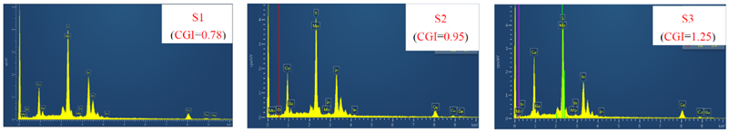
| Atomic Ratio (%) | Cu K | In L | Ga K | S K | Mo L | CGI | GGI |
|---|---|---|---|---|---|---|---|
| S1 | 21.12 | 24.63 | 2.43 | 49.03 | 2.79 | 0.78 | 0.08 |
| S2 | 24.33 | 23.05 | 2.43 | 46.6 | 3.59 | 0.95 | 0.10 |
| S3 | 27.21 | 20.68 | 0.98 | 48.75 | 2.38 | 1.25 | 0.04 |
 | |||||||
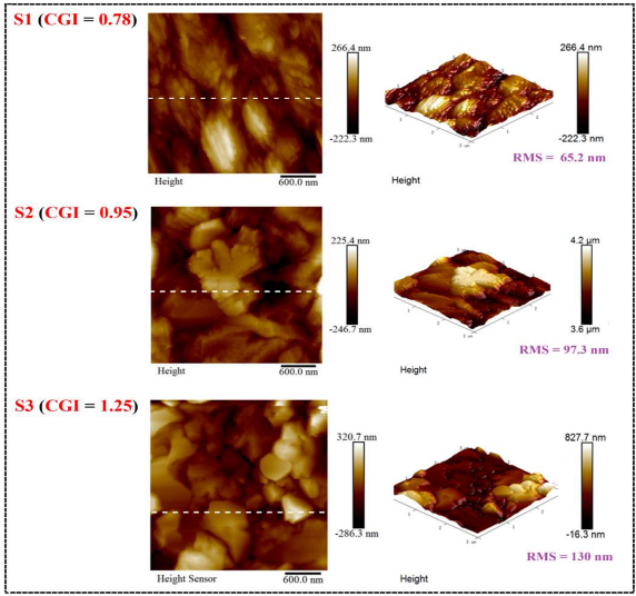
| RMS (Rq) | Ra | Rmax | |
|---|---|---|---|
| S1 (CGI = 0.78) | 65.2 nm | 50.4 nm | 407 nm |
| S2 (CGI = 0.95) | 97.3 nm | 73.4 nm | 483 nm |
| S3 (CGI = 1.25) | 130 nm | 104 nm | 785 nm |
 | |||
Disclaimer/Publisher’s Note: The statements, opinions and data contained in all publications are solely those of the individual author(s) and contributor(s) and not of MDPI and/or the editor(s). MDPI and/or the editor(s) disclaim responsibility for any injury to people or property resulting from any ideas, methods, instructions or products referred to in the content. |
© 2023 by the authors. Licensee MDPI, Basel, Switzerland. This article is an open access article distributed under the terms and conditions of the Creative Commons Attribution (CC BY) license (https://creativecommons.org/licenses/by/4.0/).
Share and Cite
Li, T.-C.; Chang, C.-W.; Tai, C.-C.; Ho, J.-J.; Hsieh, T.-P.; Liu, Y.-T.; Lu, T.-L. Optoelectronic Effects of Copper–Indium–Gallium–Sulfur (CIGS2)-Solar Cells Prepared by Three-Stage Co-Evaporation Process Technology. Micromachines 2023, 14, 1709. https://doi.org/10.3390/mi14091709
Li T-C, Chang C-W, Tai C-C, Ho J-J, Hsieh T-P, Liu Y-T, Lu T-L. Optoelectronic Effects of Copper–Indium–Gallium–Sulfur (CIGS2)-Solar Cells Prepared by Three-Stage Co-Evaporation Process Technology. Micromachines. 2023; 14(9):1709. https://doi.org/10.3390/mi14091709
Chicago/Turabian StyleLi, Tzu-Chien, Chia-Wen Chang, Chia-Chun Tai, Jyh-Jier Ho, Tung-Po Hsieh, Yung-Tsung Liu, and Tsung-Lin Lu. 2023. "Optoelectronic Effects of Copper–Indium–Gallium–Sulfur (CIGS2)-Solar Cells Prepared by Three-Stage Co-Evaporation Process Technology" Micromachines 14, no. 9: 1709. https://doi.org/10.3390/mi14091709