

High-Performance All-Optical Logic Operations Using Ψ-Shaped Silicon Waveguides at 1.55 μm


Abstract
:1. Introduction
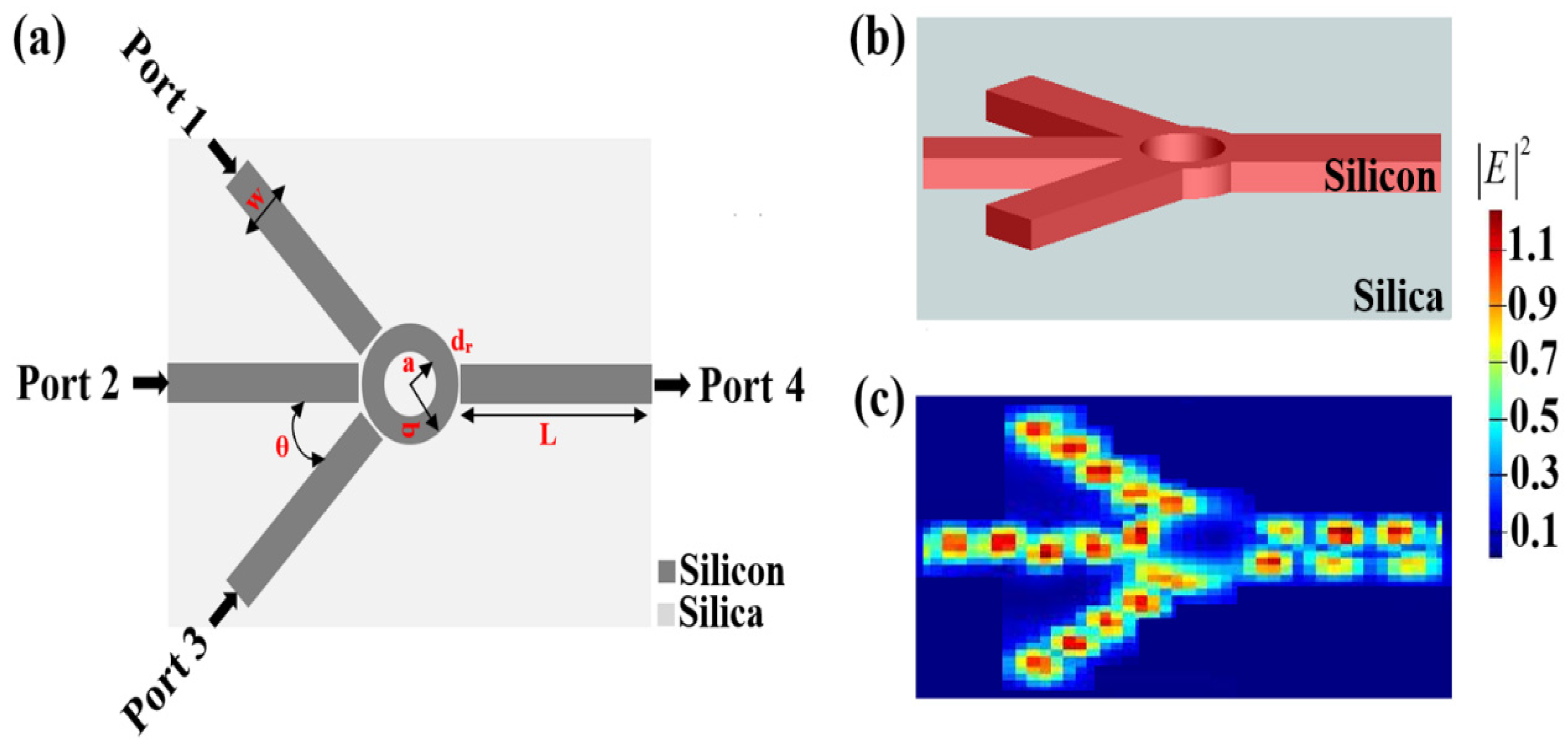
2. Ψ-Shaped Silicon Waveguide
3. Logic Operations’ Realization
3.1. XOR
3.2. AND
3.3. OR
3.4. NOT
3.5. NOR
3.6. NAND
3.7. XNOR
4. Conclusions
Author Contributions
Funding
Informed Consent Statement
Data Availability Statement
Conflicts of Interest
References
- Chen, L.R.; Wang, J.; Naghdi, B.; Glesk, I. Subwavelength grating waveguide devices for telecommunications applications. IEEE J. Sel. Top. Quantum Electron. 2019, 25, 8200111. [Google Scholar] [CrossRef]
- Lipson, M. Guiding, modulating, and emitting light on silicon—Challenges and opportunities. J. Light. Technol. 2005, 23, 4222–4238. [Google Scholar] [CrossRef]
- Vlasov, Y.A. Silicon photonics for next-generation computing systems. In Proceedings of the 34th European Conference on Optical Communications, Brussels, Belgium, 21–25 September 2008. [Google Scholar]
- Lee, B.G.; Bergmann, K. Silicon nano-photonic interconnection networks in multicore processor systems. In Frontiers in Optics 2008/Laser Science XXIV/Plasmonics and Metamaterials/Optical Fabrication and Testing; Optica Publishing Group: Washington, DC, USA, 2008. [Google Scholar]
- Thourhout, D.V.; Campenhout, J.V.; Baets, R.; Rojo-Romeo, P.; Regreny, P.; Seassal, C.; Binetti, P.; Leijtens, X.J.M.; Ntzel, R.; Smit, M.K.; et al. Photonic interconnect layer on CMOS. In Proceeding of the 33rd European Conference on Optical Communications, Berlin, Germany, 16–20 September 2007. [Google Scholar]
- Tsybeskov, L.; Lockwood, D.J.; Ichikawa, M. Silicon photonics: CMOS going optical. Proc. IEEE 2009, 97, 1161–1165. [Google Scholar] [CrossRef]
- Shi, Y.; Zhang, Y.; Wan, Y.; Yu, Y.; Zhang, Y.; Hu, X.; Xiao, X.; Xu, H.; Zhang, L.; Pan, B. Silicon photonics for high-capacity data communications. Photonics Res. 2022, 10, A106–A134. [Google Scholar] [CrossRef]
- Tsuchizawa, T.; Yamada, K.; Fukuda, H.; Watanabe, T.; Takahashi, J.; Takahashi, M.; Shoji, T.; Tamechika, E.; Itabashi, S.; Morita, H.; et al. Microphotonics devices based on silicon microfabrication technology. IEEE J. Sel. Top. Quant. Electron. 2005, 11, 232–240. [Google Scholar] [CrossRef]
- Saruwatari, A. All-optical signal processing for terabit/second optical transmission. IEEE J. Sel. Top. Quantum Electron. 2000, 6, 1363–1374. [Google Scholar] [CrossRef]
- Willner, A.E.; Khaleghi, S.; Chitgarha, M.R.; Yilmaz, O.F. All-optical signal processing. J. Lightwave Technol. 2014, 32, 660–680. [Google Scholar] [CrossRef]
- Rani, P.; Kalra, Y.; Sinha, R.K. Design of all optical logic gates in photonic crystal waveguides. Optik 2015, 126, 950–955. [Google Scholar] [CrossRef]
- Husko, C.; Vo, T.D.; Corcoran, B.; Li, J.; Krauss, T.; Eggleton, B. Ultracompact all-optical XOR logic gate in a slow-light silicon photonic crystal waveguide. Opt. Express 2011, 19, 20681–20690. [Google Scholar] [CrossRef]
- Andalib, P.; Granpayeh, N. All-optical ultracompact photonic crystal AND gate based on nonlinear ring resonators. J. Opt. Soc. Am. B 2009, 26, 10–16. [Google Scholar] [CrossRef]
- Jandieri, V.; Khomeriki, R.; Erni, D. Realization of true all-optical AND logic gate based on the nonlinear coupled air-hole type photonic crystal waveguide. Opt. Express 2018, 26, 19845–19853. [Google Scholar] [CrossRef] [PubMed]
- Ishizaka, Y.; Kawaguchi, Y.; Saitoh, K.; Koshiba, M. Design of ultracompact all-optical XOR and AND logic gates with low power consumption. Opt. Commun. 2011, 284, 3528–3533. [Google Scholar] [CrossRef]
- Priya, N.H.; Swarnakar, S.; Krishna, S.V.; Kumar, S. Design and analysis of an optical three-input AND gate using a photonic crystal fiber. Appl. Opt. 2022, 61, 77–83. [Google Scholar]
- Priya, N.H.; Swarnakar, S.; Krishna, S.V.; Kumar, S. Design and analysis of a photonic crystal-based all-optical 3-input OR gate for high-speed optical processing. Opt. Quantum Electron. 2021, 53, 720. [Google Scholar] [CrossRef]
- Rao, D.G.S.; Swarnakar, S.; Palacharla, V.; Raju, K.S.R.; Kumar, S. Design of all-optical AND, OR, and XOR logic gates using photonic crystals for switching applications. Photonic Netw. Commun. 2021, 41, 109–118. [Google Scholar] [CrossRef]
- Swarnakar, S.; Palacharla, V.; Muduli, A.; Kumar, S. Design and optimization of photonic crystal based all-optical logic gate with enhanced contrast ratio. Opt. Quantum Electron. 2023, 55, 623. [Google Scholar] [CrossRef]
- Rachana, M.; Swarnakar, S.; Babu, M.R.; Swetha, P.M.; Rangaiah, Y.P.; Krishna, S.V.; Kumar, S. Optimization of an all-optical 3-input universal logic gate with an enhanced contrast ratio by exploiting T-shaped photonic crystal waveguide. App. Opt. 2022, 61, 8162–8171. [Google Scholar] [CrossRef]
- Kita, S.; Nozaki, K.; Takata, K.; Shinya, A.; Notomi, M. Ultrashort low-loss Ψ gates for linear optical logic on Si photonics platform. Commun. Phys. 2020, 3, 33. [Google Scholar] [CrossRef]
- Zeng, S.; Zhang, Y.; Pun, E. Ultrasmall optical logic gates based on silicon periodic dielectric waveguides. Photonics Nanostr. Fundam. Appl. 2010, 8, 32. [Google Scholar] [CrossRef]
- Cui, L.; Yu, L. Multifunctional logic gates based on silicon hybrid plasmonic waveguides. Mod. Phys. Lett. B 2018, 32, 1850008. [Google Scholar] [CrossRef]
- Kotb, A.; Zoiros, K.E.; Hatziefremidis, A.; Guo, C. Optical logic gates based on Z-shaped silicon waveguides at 1.55 μm. Micromachines 2023, 14, 1266. [Google Scholar] [CrossRef] [PubMed]
- Kotb, A.; Zoiros, K.E.; Li, W. Silicon-on-silica waveguides-based all-optical logic gates at 1.55 μm. Phys. Scr. 2023, 98, 035517. [Google Scholar] [CrossRef]
- Kotb, A.; Yao, C. All-optical logic operations based on silicon-on-insulator waveguides. Opt. Eng. 2023, 62, 048101. [Google Scholar] [CrossRef]
- Kotb, A.; Zoiros, K.E. 2 × 2 compact silicon waveguide-based optical logic functions at 1.55 μm. Photonics 2023, 10, 403. [Google Scholar] [CrossRef]
- Kotb, A.; Zoiros, K.E.; Guo, C. All-optical logic gates using E-shaped silicon waveguides at 1.55 μm. J. App. Phys. 2023, 133, 173101. [Google Scholar] [CrossRef]
- Gao, L.; Chen, L.; Wei, H.; Xu, H. Lithographically fabricated gold nanowire waveguides for plasmonic routers and logic gates. Nanoscale 2018, 10, 14771. [Google Scholar] [CrossRef]
- Nozhat, N.; Alikomak, H.; Khodadadi, M. All-optical XOR and NAND logic gates based on plasmonic nanoparticles. Opt. Commun. 2017, 392, 208–213. [Google Scholar] [CrossRef]
- Pan, D.; Wei, H.; Xu, H. Optical interferometric logic gates based on metal slot waveguide network realizing whole fundamental logic operations. Opt. Express 2013, 21, 9556. [Google Scholar] [CrossRef]
- Bian, Y.; Gong, Q. Compact all-optical interferometric logic gates based on one-dimensional metal-insulator-metal structures. Opt. Commun. 2014, 313, 27–35. [Google Scholar] [CrossRef]
- Al-Musawi, H.K.; Al-Janabi, A.K.; Al-Abassi, S.A.W.; Abusiba, N.A.A.; Al-Fatlawi, N.A.Q. Plasmonic logic gates based on dielectric-metal-dielectric design with two optical communication bands. Optik 2020, 223, 165416. [Google Scholar] [CrossRef]
- Yao, C.; Kotb, A.; Wang, B.; Singh, S.; Guo, C. All-optical logic gates using dielectric-loaded waveguides with quasi-rhombus metasurfaces. Opt. Lett. 2020, 45, 3769–3772. [Google Scholar] [CrossRef] [PubMed]
- Keshtkar, P.; Miri, M.; Yasrebi, N. Low power, high speed, all-optical logic gates based on optical bistability in graphene-containing compact microdisk resonators. Appl. Opt. 2021, 60, 7234–7242. [Google Scholar] [CrossRef] [PubMed]
- Kotb, A.; Guo, C. 100 Gb/s all-optical multifunctional AND, XOR, NOR, OR, XNOR, and NAND logic gates in a single compact scheme based on semiconductor optical amplifiers. Opt. Laser Technol. 2021, 137, 106828. [Google Scholar] [CrossRef]
- Available online: www.lumerical.com/tcadproducts/fdtd/ (accessed on 31 December 2018).
- Laakso, I.; Ilvonen, S.; Uusitupa, T. Performance of convolutional PML absorbing boundary conditions in finite-difference time-domain SAR calculations. Phys. Med. Biol. 2007, 52, 7183–7192. [Google Scholar] [CrossRef]
- Sahu, P.P. Theoretical investigation of all optical switch based on compact surface plasmonic two mode interference coupler. J. Lightwave Technol. 2016, 34, 1300–1305. [Google Scholar] [CrossRef]
- Smith, B.J.; Kundys, D.; Thomas-Peter, N.; Smith, P.G.R.; Walmsley, I.A. Phase-controlled integrated photonic quantum circuits. Opt. Express 2009, 17, 13516–13525. [Google Scholar] [CrossRef]
- Wang, Y.; Tian, Z.; Li, Y.; Zhang, Z.; Wang, L.; Chen, Q. Phase customization in photonic integrated circuits with trimmed waveguides. Opt. Lett. 2022, 47, 5889–5892. [Google Scholar] [CrossRef]
- Li, M.; Li, C.; Chen, Y.; Feng, L.; Yan, L.; Zhang, Q.; Bao, J.; Liu, B.; Ren, X.; Jianwei Wang, J.; et al. On-chip path encoded photonic quantum Toffoli gate. Photonics Res. 2022, 10, 1533–1542. [Google Scholar] [CrossRef]
- Klauck, F.; Heinrich, M.; Szameit, A. Photonic two-particle quantum walks in Su–Schrieffer–Heeger lattices. Photonics Res. 2021, 9, A1–A7. [Google Scholar] [CrossRef]
- Zhang, Q.; Li, M.; Xu, J.; Lin, Z.; Yu, H.; Wang, M.; Fang, Z.; Cheng, Y.; Gong, Q.; Li, Y. Reconfigurable directional coupler in lithium niobate crystal fabricated by three-dimensional femtosecond laser focal field engineering. Photonics Res. 2019, 7, 503–507. [Google Scholar] [CrossRef]
- Anton, C.; Loredo, J.C.; Coppola, G.; Ollivier, H.; Viggianiello, N.; Harouri, A.; Somaschi, N.; Crespi, A.; Sagnes, I.; Lemaitre, A.; et al. Interfacing scalable photonic platforms: Solid-state based multi-photon interference in a reconfigurable glass chip. Optica 2019, 6, 1471–1477. [Google Scholar] [CrossRef]
- Atzeni, S.; Rab, A.S.; Corrielli, G.; Polino, E.; Valeri, M.; Mataloni, P.; Spagnolo, N.; Crespi, A.; Sciarrino, F.; Osellame, R. Integrated sources of entangled photons at the telecom wavelength in femtosecond-laser-written circuits. Optica 2018, 5, 311–314. [Google Scholar] [CrossRef]
- Wei, D.; Wang, C.; Wang, H.; Hu, X.; Wei, D.; Fang, X.; Zhang, Y.; Wu, D.; Hu, Y.; Li, J.; et al. Experimental demonstration of a three-dimensional lithium niobate nonlinear photonic crystal. Nat. Photonics 2018, 12, 596–600. [Google Scholar] [CrossRef]
- Marshall, G.D.; Politi, A.; Matthews, J.C.F.; Dekker, P.; Ams, M.; Withford, M.J.; O’Brien, J.L. Laser written waveguide photonic quantum circuits. Opt. Express 2009, 17, 12546–12554. [Google Scholar] [CrossRef] [PubMed]
- Passaro, V.M.N.; Notte, M.L. Optimizing SOI slot waveguide fabrication tolerances and strip-slot coupling for very efficient optical sensing. Sensors 2012, 12, 2436–2455. [Google Scholar] [CrossRef]
- Prinzen, A.; Waldow, M.; Kurz, H. Fabrication tolerances of SOI based directional couplers and ring resonators. Opt. Express 2013, 21, 17212–17220. [Google Scholar] [CrossRef]
- Available online: https://www.edmundoptics.com/p/1550nm-0-250mw-fiber-coupled-laser/12219/ (accessed on 31 December 2018).
- Al-Hetara, A.M.; Shamsan, Z.A. Optical wavelength and dimensions tolerance criterion for multimode interference couplers. WSEAS Tran. Commun. 2014, 13, 567–571. [Google Scholar]
- Zhang, Z.; Wang, Y.; Tsang, H.K. Experimental study of dependence of waveguide array phase errors on waveguide width. In Proceedings of the Asia Communications and Photonics Conference (ACP), Chengdu, China, 2–5 November 2019; pp. 1–3. [Google Scholar]
- Han, Q.; Robin, D.; Gervais, A.; Ménard, M.; Shi, W. Phase errors and statistical analysis of silicon-nitride arrayed waveguide gratings. Opt. Express 2022, 30, 42784–42800. [Google Scholar] [CrossRef]
- Khan, U.; Fiers, M.; Xing, Y.; Bogaerts, W. Experimental phase error extraction and modelling in silicon photonic arrayed waveguide gratings. Proc. SPIE 2020, 11285, 1128510. [Google Scholar]
- Goh, T.; Suzuki, S.; Sugita, A. Estimation of waveguide phase error in silica-based waveguides. J. Light. Technol. 1997, 15, 2107–2113. [Google Scholar] [CrossRef]
- Zhang, L.; Yue, Y.; Beausoleil, R.C.; Willner, A.E. Flattened dispersion in Si slot waveguides. Opt. Express 2010, 18, 20529–20534. [Google Scholar] [CrossRef]
- Hu, Y.; Yang, Z.; Chen, N.; Hu, H.; Zhang, B.; Yang, H.; Lu, X.; Zhang, X.; Xu, J. 3x40 Gbit/s all-optical logic operation based on low-loss triple-mode silicon waveguide. Micromachines 2022, 13, 90. [Google Scholar] [CrossRef] [PubMed]
- Crisp, J.; Elliott, B. Introduction to Fiber Optics, 3rd ed.; Elsevier: Amsterdam, The Netherlands, 2005. [Google Scholar]
- Donzella, V.; Sherwali, A.; Flueckiger, J.; Grist, S.M.; Fard, S.T.; Chrostowski, L. Design and fabrication of SOI micro-ring resonators based on sub-wavelength grating waveguides. Opt. Express 2015, 23, 4791–4803. [Google Scholar] [CrossRef]
- Fu, Y.; Hu, X.; Lu, C.; Yue, S.; Yang, H.; Gong, Q. All-optical logic gates based on nanoscale plasmonic slot waveguides. Nano Lett. 2012, 12, 5784–5790. [Google Scholar] [CrossRef] [PubMed]
- Chen, X.; Huo, L.; Zhao, Z.; Zhuang, L.; Lou, C. Study on 100-Gb/s reconfigurable all-optical logic gates using a single semiconductor optical amplifier. Opt. Express 2016, 24, 30245–30253. [Google Scholar] [CrossRef] [PubMed]
- Dong, H.; Sun, H.; Wang, Q.; Dutta, N.K.; Jaques, J. 80 Gb/s All-optical logic AND operation using Mach-Zehnder interferometer with differential scheme. Opt. Commun. 2006, 265, 79–83. [Google Scholar] [CrossRef]
- Wang, Q.; Zhu, G.; Chen, H.; Jaques, J.; Leuthold, J.; Piccirilli, A.B.; Dutta, N.K. Study of all-optical XOR using Mach–Zehnder interferometer and differential scheme. IEEE J. Quantum Electron. 2004, 40, 703–710. [Google Scholar] [CrossRef]


| Symbol | Definition | Value | Unit |
|---|---|---|---|
| L | Length of slot | 1.0 | μm |
| w | Width of slot | 0.3 | μm |
| d | Thickness of slot | 0.3 | μm |
| a | Microring inner radius | 0.2 | μm |
| b | Microring outer radius | 0.3 | μm |
| dr | Distance between slot and microring | 0.01 | μm |
| θ | Angle between slots | 45 | degree |
| λ | Operating wavelength | 1.55 | μm |
| Tth | Threshold transmission | 0.2 | - |
| Port 1 | Port 3 | Port 2 (REF) | T | Port 4 (Output) | CR (dB) |
|---|---|---|---|---|---|
| 0 | 0 | 1 | 0.027 | 0 | 27 |
| 0 | 1 | 1 | 0.485 | 1 | |
| 1 | 0 | 1 | 0.442 | 1 | |
| 1 | 1 | 1 | 0.035 | 0 |
| Port 1 | Port 3 | Port 2 (REF) | T | Port 4 (Output) | CR (dB) |
|---|---|---|---|---|---|
| 0 | 0 | 1 | 0.027 | 0 | 28.28 |
| 0 | 1 | 1 | 0.038 | 0 | |
| 1 | 0 | 1 | 0.038 | 0 | |
| 1 | 1 | 1 | 0.575 | 1 |
| Port 1 | Port 3 | Port 2 (REF) | T | Port 4 (Output) | CR (dB) |
|---|---|---|---|---|---|
| 0 | 0 | 1 | 0.027 | 0 | 31 |
| 0 | 1 | 1 | 0.485 | 1 | |
| 1 | 0 | 1 | 0.442 | 1 | |
| 1 | 1 | 1 | 0.865 | 1 |
| Operation | CR (dB) With REF | CR (dB) Without REF |
|---|---|---|
| XOR | 27 | 7.2 |
| AND | 28.28 | 8.5 |
| OR | 31 | 9.7 |
| Port 1 (Clk) | Port 3 | T | Port 4 (Output) | CR (dB) |
|---|---|---|---|---|
| 1 | 1 | 0.023 | 0 | 25.17 |
| 1 | 0 | 0.285 | 1 |
| Port 1 (Clk) | Port 2 | Port 3 | T | Port 4 (Output) | CR (dB) |
|---|---|---|---|---|---|
| 1 | 0 | 0 | 0.285 | 1 | 27.24 |
| 1 | 0 | 1 | 0.019 | 0 | |
| 1 | 1 | 0 | 0.020 | 0 | |
| 1 | 1 | 1 | 0.017 | 0 |
| Port 1 (Clk) | Port 2 | Port 3 | T | Port 4 (Output) | CR (dB) |
|---|---|---|---|---|---|
| 1 | 0 | 0 | 0.285 | 1 | 34.10 |
| 1 | 0 | 1 | 0.845 | 1 | |
| 1 | 1 | 0 | 0.412 | 1 | |
| 1 | 1 | 1 | 0.017 | 0 |
| Port 1 (Clk) | Port 2 | Port 3 | T | Port 4 (Output) | CR (dB) |
|---|---|---|---|---|---|
| 1 | 0 | 0 | 0.285 | 1 | 33.84 |
| 1 | 0 | 1 | 0.019 | 0 | |
| 1 | 1 | 0 | 0.020 | 0 | |
| 1 | 1 | 1 | 0.865 | 1 |
| Functions | Waveguide | Wavelength (nm) | CR (dB) | Ref. |
|---|---|---|---|---|
| AND, XOR, OR, NOT, NAND, NOR XNOR | PC waveguides | 1550 | 5.42–9.59 | [11] |
| AND, XOR, XNOR | T-shaped PC waveguides | 1550 | 8.29–33.05 | [16,17,18] |
| AND, NOR, XNOR | Silicon photonics platform | 1550 | >10 dB | [21] |
| XOR, AND, OR, NOT, NOR, XNOR, NAND | Silicon-on-silica waveguides | 1550 | 20.51–30.33 | [25] |
| XOR, AND, OR, NOT, NOR, XNOR, NAND | Silicon-on-silica waveguides | 1330 | 11.76–32.73 | [26] |
| XOR, NAND | Gold disk-shaped nanoparticles | 451.8 | 24 and 26 | [30] |
| NOT, XOR, AND, OR, NOR, NAND, XNOR | Metal slot waveguide | 632.8 | 6–16 | [31] |
| NOT, XOR, AND, OR, NOR, NAND, XNOR | Metal–insulator–metal structures | 632.8 | 15 | [32] |
| NOT, XOR, AND, OR, NOR, NAND, XNOR | Dielectric–metal–dielectric design | 900 and 1330 | 5.37–22 | [33] |
| XOR, AND, OR, NOR, NAND, XNOR | Dielectric-loaded waveguides | 471 | 24.41–33.39 | [34] |
| XOR, AND, OR, NOT, NOR, XNOR, NAND | Ψ silicon waveguides | 1550 | 25.17–34.10 | This work |
Disclaimer/Publisher’s Note: The statements, opinions and data contained in all publications are solely those of the individual author(s) and contributor(s) and not of MDPI and/or the editor(s). MDPI and/or the editor(s) disclaim responsibility for any injury to people or property resulting from any ideas, methods, instructions or products referred to in the content. |
© 2023 by the authors. Licensee MDPI, Basel, Switzerland. This article is an open access article distributed under the terms and conditions of the Creative Commons Attribution (CC BY) license (https://creativecommons.org/licenses/by/4.0/).
Share and Cite
Kotb, A.; Zoiros, K.E.; Guo, C. High-Performance All-Optical Logic Operations Using Ψ-Shaped Silicon Waveguides at 1.55 μm. Micromachines 2023, 14, 1793. https://doi.org/10.3390/mi14091793
Kotb A, Zoiros KE, Guo C. High-Performance All-Optical Logic Operations Using Ψ-Shaped Silicon Waveguides at 1.55 μm. Micromachines. 2023; 14(9):1793. https://doi.org/10.3390/mi14091793
Chicago/Turabian StyleKotb, Amer, Kyriakos E. Zoiros, and Chunlei Guo. 2023. "High-Performance All-Optical Logic Operations Using Ψ-Shaped Silicon Waveguides at 1.55 μm" Micromachines 14, no. 9: 1793. https://doi.org/10.3390/mi14091793
APA StyleKotb, A., Zoiros, K. E., & Guo, C. (2023). High-Performance All-Optical Logic Operations Using Ψ-Shaped Silicon Waveguides at 1.55 μm. Micromachines, 14(9), 1793. https://doi.org/10.3390/mi14091793