Analysis of Nanowire pn-Junction with Combined Current–Voltage, Electron-Beam-Induced Current, Cathodoluminescence, and Electron Holography Characterization
Abstract
:1. Introduction
2. Materials and Methods
2.1. Nanowire Growth
2.2. IV and EBIC Measurements with Nanoprobe Contacting
2.3. CL Characterization
2.4. Electron Holography Characterization
2.5. Drift-Diffusion Modelling
2.5.1. Mobility
2.5.2. Recombination
3. Results and Discussion
3.1. IV Measurements
3.2. Electron Holography
3.3. EBIC Measurements
3.4. Dependence of CL Intensity along Nanowire Axis and Comparison to EBIC Signal
3.5. Extraction of Doping Concentration from CL Measurements
3.6. Analysis of Characterization Results with the Help of Drift-Diffusion Model
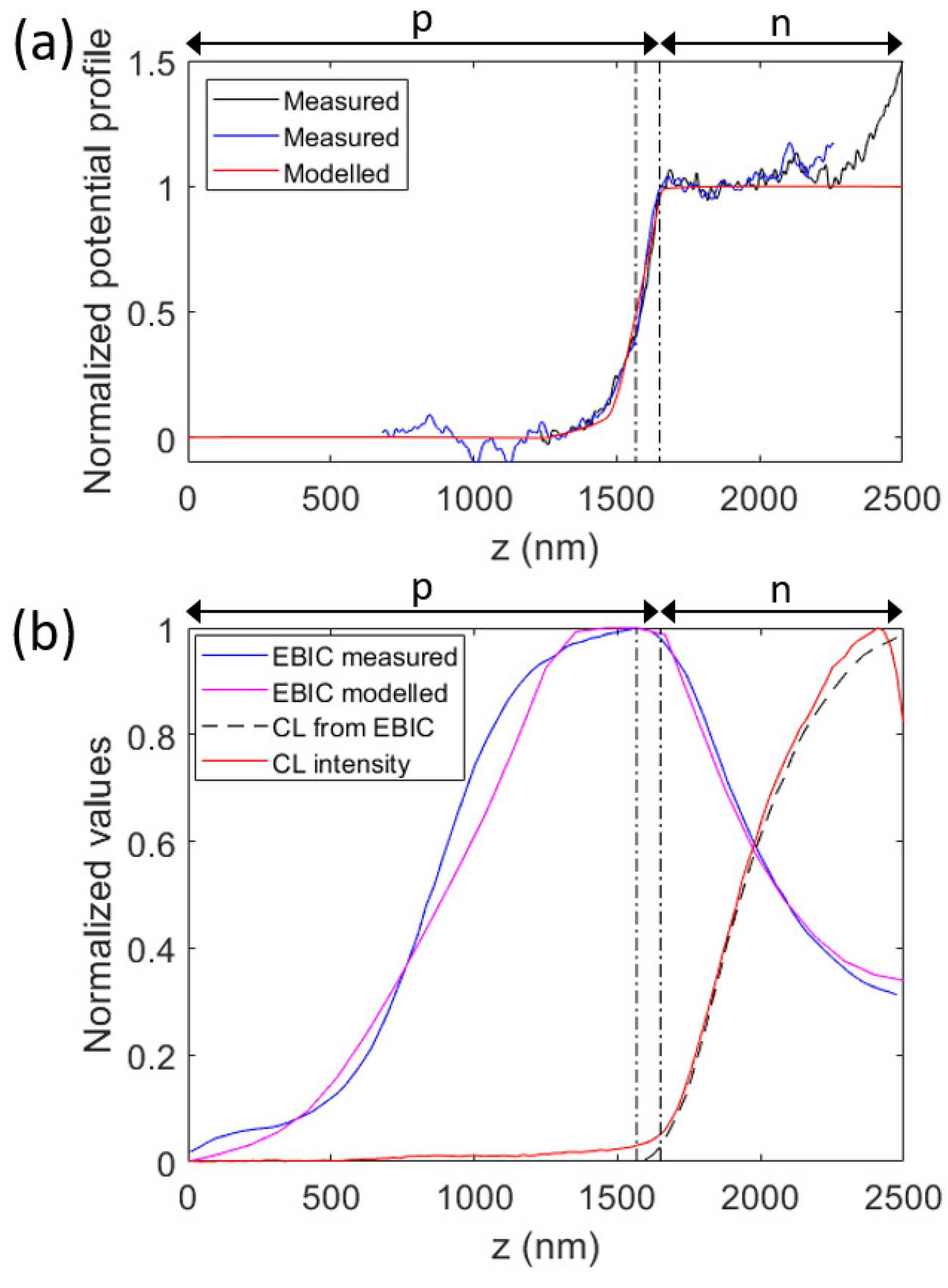
- We assume a transition to the n type region at z = 1650 nm, with ND(z) having the rather constant value of 2.4 × 1018 cm−3, with exact values provided from the CL characterization (see Figure S2 in the Supplementary Materials). For this n region, we assume a constant τrec. This assumption of a constant τrec is motivated by the good agreement in Section 3.2 between the CL intensity profile and the modelled values from the EBIC profile that also used the assumption of a constant ND and τrec on the n side (producing the dashed line in Figure 3b).
- We assume an FSB at the top of the nanowire, as indicated by the EBIC profile which stays at a value of >0.3 there, instead of dropping to zero as expected if no FSB was present (as discussed in Section 3.2). We include this FSB in the model through an n-doped AlGaAs segment at z > 2500 nm before the top contact, which is placed at z = 2600 nm.
- For the p-type region, we use the NA(z) extracted from the CL measurements (see Figure S2 in the Supplementary Materials) for 0 < z < 1250 nm. This value of z = 1250 nm is motivated by the growth recipe described in Section 2.1 where the dopant is switched from p type to n type nominally at this value for z. Furthermore, the potential profile from the electron holography starts to vary from a flat profile at this z = 1250 nm (Figure 3a). Importantly, if we use the NA extracted from CL also for 1250 < z < 1500 nm, we are unable to reproduce the electron holography and the EBIC profiles (see Figures S3 and S4 in the Supplementary Materials).
4. Conclusions
Supplementary Materials
Author Contributions
Funding
Data Availability Statement
Acknowledgments
Conflicts of Interest
References
- Björk, M.T.; Ohlsson, B.J.; Sass, T.; Persson, A.I.; Thelander, C.; Magnusson, M.H.; Deppert, K.; Wallenberg, L.R.; Samuelson, L. One-Dimensional Heterostructures in Semiconductor Nanowhiskers. Appl. Phys. Lett. 2002, 80, 1058–1060. [Google Scholar] [CrossRef]
- Dick, K.A. A Review of Nanowire Growth Promoted by Alloys and Non-Alloying Elements with Emphasis on Au-Assisted III–V Nanowires. Prog. Cryst. Growth Charact. Mater. 2008, 54, 138–173. [Google Scholar] [CrossRef]
- Barrigón, E.; Heurlin, M.; Bi, Z.; Monemar, B.; Samuelson, L. Synthesis and Applications of III–V Nanowires. Chem. Rev. 2019, 119, 9170–9220. [Google Scholar] [CrossRef]
- Yan, R.; Gargas, D.; Yang, P. Nanowire Photonics. Nat. Photonics 2009, 3, 569–576. [Google Scholar] [CrossRef]
- Gudiksen, M.S.; Lauhon, L.J.; Wang, J.; Smith, D.C.; Lieber, C.M. Growth of Nanowire Superlattice Structures for Nanoscale Photonics and Electronics. Nature 2002, 415, 617–620. [Google Scholar] [CrossRef] [PubMed]
- LaPierre, R.R.; Chia, A.C.E.; Gibson, S.J.; Haapamaki, C.M.; Boulanger, J.; Yee, R.; Kuyanov, P.; Zhang, J.; Tajik, N.; Jewell, N.; et al. III–V Nanowire Photovoltaics: Review of Design for High Efficiency. Phys. Status Solidi RRL—Rapid Res. Lett. 2013, 7, 815–830. [Google Scholar] [CrossRef]
- Otnes, G.; Borgström, M.T. Towards High Efficiency Nanowire Solar Cells. Nano Today 2017, 12, 31–45. [Google Scholar] [CrossRef]
- Goktas, N.I.; Wilson, P.; Ghukasyan, A.; Wagner, D.; McNamee, S.; LaPierre, R.R. Nanowires for Energy. Appl. Phys. Rev. 2018, 5, 041305. [Google Scholar] [CrossRef]
- Li, Z.; Tan, H.H.; Jagadish, C.; Fu, L. III–V Semiconductor Single Nanowire Solar Cells: A Review. Adv. Mater. Technol. 2018, 3, 1800005. [Google Scholar] [CrossRef]
- Cui, Y.; Wang, J.; Plissard, S.R.; Cavalli, A.; Vu, T.T.T.; van Veldhoven, R.P.J.; Gao, L.; Trainor, M.; Verheijen, M.A.; Haverkort, J.E.M.; et al. Efficiency Enhancement of InP Nanowire Solar Cells by Surface Cleaning. Nano Lett. 2013, 13, 4113–4117. [Google Scholar] [CrossRef]
- Krogstrup, P.; Jørgensen, H.I.; Heiss, M.; Demichel, O.; Holm, J.V.; Aagesen, M.; Nygard, J.; Fontcuberta i Morral, A. Single-Nanowire Solar Cells beyond the Shockley–Queisser Limit. Nat. Photonics 2013, 7, 306–310. [Google Scholar] [CrossRef]
- Yao, M.; Cong, S.; Arab, S.; Huang, N.; Povinelli, M.L.; Cronin, S.B.; Dapkus, P.D.; Zhou, C. Tandem Solar Cells Using GaAs Nanowires on Si: Design, Fabrication, and Observation of Voltage Addition. Nano Lett. 2015, 15, 7217–7224. [Google Scholar] [CrossRef] [PubMed]
- VJ, L.; Oh, J.; Nayak, A.P.; Katzenmeyer, A.M.; Gilchrist, K.H.; Grego, S.; Kobayashi, N.P.; Wang, S.-Y.; Talin, A.A.; Dhar, N.K.; et al. A Perspective on Nanowire Photodetectors: Current Status, Future Challenges, and Opportunities. IEEE J. Sel. Top. Quantum Electron. 2011, 17, 1002–1032. [Google Scholar] [CrossRef]
- LaPierre, R.R.; Robson, M.; Azizur-Rahman, K.M.; Kuyanov, P. A Review of III–V Nanowire Infrared Photodetectors and Sensors. J. Phys. Appl. Phys. 2017, 50, 123001. [Google Scholar] [CrossRef]
- Mukai, T. Recent Progress in Group-III Nitride Light-Emitting Diodes. IEEE J. Sel. Top. Quantum Electron. 2002, 8, 264–270. [Google Scholar] [CrossRef]
- Sze, S.M.; Li, Y.; Ng, K.K. Physics of Semiconductor Devices; John Wiley & Sons: Hoboken, NJ, USA, 2021; ISBN 978-1-119-61800-3. [Google Scholar]
- Wallentin, J.; Borgström, M.T. Doping of Semiconductor Nanowires. J. Mater. Res. 2011, 26, 2142–2156. [Google Scholar] [CrossRef]
- Chen, Y.; Kivisaari, P.; Pistol, M.-E.; Anttu, N. Optimization of the Short-Circuit Current in an InP Nanowire Array Solar Cell through Opto-Electronic Modeling. Nanotechnology 2016, 27, 435404. [Google Scholar] [CrossRef]
- Chen, Y.; Kivisaari, P.; Pistol, M.-E.; Anttu, N. Optimized Efficiency in InP Nanowire Solar Cells with Accurate 1D Analysis. Nanotechnology 2017, 29, 045401. [Google Scholar] [CrossRef]
- Otnes, G.; Barrigón, E.; Sundvall, C.; Svensson, K.E.; Heurlin, M.; Siefer, G.; Samuelson, L.; Åberg, I.; Borgström, M.T. Understanding InP Nanowire Array Solar Cell Performance by Nanoprobe-Enabled Single Nanowire Measurements. Nano Lett. 2018, 18, 3038–3046. [Google Scholar] [CrossRef]
- Barrigón, E.; Zhang, Y.; Hrachowina, L.; Otnes, G.; Borgström, M.T. Unravelling Processing Issues of Nanowire-Based Solar Cell Arrays by Use of Electron Beam Induced Current Measurements. Nano Energy 2020, 71, 104575. [Google Scholar] [CrossRef]
- Gao, Q.; Li, Z.; Li, L.; Vora, K.; Li, Z.; Alabadla, A.; Wang, F.; Guo, Y.; Peng, K.; Wenas, Y.C.; et al. Axial p-n Junction Design and Characterization for InP Nanowire Array Solar Cells. Prog. Photovolt. Res. Appl. 2019, 27, 237–244. [Google Scholar] [CrossRef]
- Piazza, V.; Wirths, S.; Bologna, N.; Ahmed, A.A.; Bayle, F.; Schmid, H.; Julien, F.; Tchernycheva, M. Nanoscale Analysis of Electrical Junctions in InGaP Nanowires Grown by Template-Assisted Selective Epitaxy. Appl. Phys. Lett. 2019, 114, 103101. [Google Scholar] [CrossRef]
- Saket, O.; Himwas, C.; Piazza, V.; Bayle, F.; Cattoni, A.; Oehler, F.; Patriarche, G.; Travers, L.; Collin, S.; Julien, F.H.; et al. Nanoscale Electrical Analyses of Axial-Junction GaAsP Nanowires for Solar Cell Applications. Nanotechnology 2020, 31, 145708. [Google Scholar] [CrossRef] [PubMed]
- Yang, M.; Darbandi, A.; Watkins, S.P.; Kavanagh, K.L. Geometric Effects on Carrier Collection in Core–Shell Nanowire p–n Junctions. Nano Futur. 2021, 5, 025007. [Google Scholar] [CrossRef]
- Dastjerdi, M.H.T.; Fiordaliso, E.M.; Leshchenko, E.D.; Akhtari-Zavareh, A.; Kasama, T.; Aagesen, M.; Dubrovskii, V.G.; LaPierre, R.R. Three-Fold Symmetric Doping Mechanism in GaAs Nanowires. Nano Lett. 2017, 17, 5875–5882. [Google Scholar] [CrossRef]
- Wolf, D.; Hübner, R.; Niermann, T.; Sturm, S.; Prete, P.; Lovergine, N.; Büchner, B.; Lubk, A. Three-Dimensional Composition and Electric Potential Mapping of III–V Core–Multishell Nanowires by Correlative STEM and Holographic Tomography. Nano Lett. 2018, 18, 4777–4784. [Google Scholar] [CrossRef]
- Pennington, R.S.; Boothroyd, C.B.; Dunin-Borkowski, R.E. Surface Effects on Mean Inner Potentials Studied Using Density Functional Theory. Ultramicroscopy 2015, 159, 34–45. [Google Scholar] [CrossRef] [PubMed]
- Barrigón, E.; Hultin, O.; Lindgren, D.; Yadegari, F.; Magnusson, M.H.; Samuelson, L.; Johansson, L.I.M.; Björk, M.T. GaAs Nanowire pn-Junctions Produced by Low-Cost and High-Throughput Aerotaxy. Nano Lett. 2018, 18, 1088–1092. [Google Scholar] [CrossRef]
- Prete, P.; Wolf, D.; Marzo, F.; Lovergine, N. Nanoscale Spectroscopic Imaging of GaAs-AlGaAs Quantum Well Tube Nanowires: Correlating Luminescence with Nanowire Size and Inner Multishell Structure. Nanophotonics 2019, 8, 1567–1577. [Google Scholar] [CrossRef]
- Vermeersch, R.; Jacopin, G.; Robin, E.; Pernot, J.; Gayral, B.; Daudin, B. Optical Properties of Ga-Doped AlN Nanowires. Appl. Phys. Lett. 2023, 122, 091106. [Google Scholar] [CrossRef]
- Åberg, I.; Vescovi, G.; Asoli, D.; Naseem, U.; Gilboy, J.P.; Sundvall, C.; Dahlgren, A.; Svensson, K.E.; Anttu, N.; Björk, M.T.; et al. A GaAs Nanowire Array Solar Cell With 15.3% Efficiency at 1 Sun. IEEE J. Photovolt. 2016, 6, 185–190. [Google Scholar] [CrossRef]
- Vurgaftman, I.; Meyer, J.R.; Ram-Mohan, L.R. Band Parameters for III–V Compound Semiconductors and Their Alloys. J. Appl. Phys. 2001, 89, 5815–5875. [Google Scholar] [CrossRef]
- Sotoodeh, M.; Khalid, A.H.; Rezazadeh, A.A. Empirical Low-Field Mobility Model for III–V Compounds Applicable in Device Simulation Codes. J. Appl. Phys. 2000, 87, 2890–2900. [Google Scholar] [CrossRef]
- Anttu, N. Physics and Design for 20% and 25% Efficiency Nanowire Array Solar Cells. Nanotechnology 2018, 30, 074002. [Google Scholar] [CrossRef] [PubMed]
- Kim, W.; Güniat, L.; Fontcuberta i Morral, A.; Piazza, V. Doping Challenges and Pathways to Industrial Scalability of III–V Nanowire Arrays. Appl. Phys. Rev. 2021, 8, 011304. [Google Scholar] [CrossRef]
- Hudait, M.K.; Modak, P.; Hardikar, S.; Krupanidhi, S.B. Zn Incorporation and Band Gap Shrinkage in p-Type GaAs. J. Appl. Phys. 1997, 82, 4931–4937. [Google Scholar] [CrossRef]
- Arab, S.; Yao, M.; Zhou, C.; Daniel Dapkus, P.; Cronin, S.B. Doping Concentration Dependence of the Photoluminescence Spectra of n-Type GaAs Nanowires. Appl. Phys. Lett. 2016, 108, 182106. [Google Scholar] [CrossRef]
- Cusano, D.A. Radiative Recombination from GaAs Directly Excited by Electron Beams. Solid State Commun. 1964, 2, 353–358. [Google Scholar] [CrossRef]
- Yablonovitch, E.; Skromme, B.J.; Bhat, R.; Harbison, J.P.; Gmitter, T.J. Band Bending, Fermi Level Pinning, and Surface Fixed Charge on Chemically Prepared GaAs Surfaces. Appl. Phys. Lett. 1989, 54, 555–557. [Google Scholar] [CrossRef]


| Quantity | Value |
|---|---|
Disclaimer/Publisher’s Note: The statements, opinions and data contained in all publications are solely those of the individual author(s) and contributor(s) and not of MDPI and/or the editor(s). MDPI and/or the editor(s) disclaim responsibility for any injury to people or property resulting from any ideas, methods, instructions or products referred to in the content. |
© 2024 by the authors. Licensee MDPI, Basel, Switzerland. This article is an open access article distributed under the terms and conditions of the Creative Commons Attribution (CC BY) license (https://creativecommons.org/licenses/by/4.0/).
Share and Cite
Anttu, N.; Fiordaliso, E.M.; Garcia, J.C.; Vescovi, G.; Lindgren, D. Analysis of Nanowire pn-Junction with Combined Current–Voltage, Electron-Beam-Induced Current, Cathodoluminescence, and Electron Holography Characterization. Micromachines 2024, 15, 157. https://doi.org/10.3390/mi15010157
Anttu N, Fiordaliso EM, Garcia JC, Vescovi G, Lindgren D. Analysis of Nanowire pn-Junction with Combined Current–Voltage, Electron-Beam-Induced Current, Cathodoluminescence, and Electron Holography Characterization. Micromachines. 2024; 15(1):157. https://doi.org/10.3390/mi15010157
Chicago/Turabian StyleAnttu, Nicklas, Elisabetta Maria Fiordaliso, José Cano Garcia, Giuliano Vescovi, and David Lindgren. 2024. "Analysis of Nanowire pn-Junction with Combined Current–Voltage, Electron-Beam-Induced Current, Cathodoluminescence, and Electron Holography Characterization" Micromachines 15, no. 1: 157. https://doi.org/10.3390/mi15010157
APA StyleAnttu, N., Fiordaliso, E. M., Garcia, J. C., Vescovi, G., & Lindgren, D. (2024). Analysis of Nanowire pn-Junction with Combined Current–Voltage, Electron-Beam-Induced Current, Cathodoluminescence, and Electron Holography Characterization. Micromachines, 15(1), 157. https://doi.org/10.3390/mi15010157


