Article

A High-Accuracy RC Time Constant Auto-Tuning Scheme for Integrated Continuous-Time Filters

1
School of Microelectronic, Xidian University, Xi’an 710071, China
2
School of Computer Science, Xi’an Shiyou University, Xi’an 710071, China
3
School of Microelectronics, Northwestern Polytechnical University, No. 127 West Youyi Road, Xi’an 710072, China
4
Guangzhou Quanshengwei Information Technology Co., Ltd., No. 18 Kexue Avenue, Huangpu District, Guangzhou 510700, China
*
Author to whom correspondence should be addressed.
Micromachines 2024, 15(1), 166; https://doi.org/10.3390/mi15010166
Submission received: 20 December 2023 / Revised: 18 January 2024 / Accepted: 19 January 2024 / Published: 22 January 2024
(This article belongs to the Special Issue High-Reliability Semiconductor Devices and Integrated Circuits)

Abstract

:
The reliability of the resistor-capacitor (RC) time constant of a continuous-time (CT) filter has long been an obstacle with integrated circuits. Due to process and temperature variations in complementary metal-oxide semiconductor (CMOS) technology, the absolute value of the RC time constant may vary over ±50%, which is a big issue for many integrated continuous-time analog circuits. This study proposes an on-chip RC time constant auto-tuning scheme. The proposed scheme is based on the discrete master–slave auto-tuning concept. Considering the limitations in conventional works, a higher tuning accuracy is achieved by adopting two techniques: firstly, parasitic capacitance cancelation is proposed to eliminate the effects caused by parasitic capacitance; secondly, symmetric comparison is introduced to minimize the influence of the DC offset of the comparator. A successive approximation procedure is applied to improve the tuning speed. The proposed auto-tuning scheme has been validated in 55 nm CMOS technology with a fourth-order active-RC low-pass filter under PVT variations and 60 mV input offset voltage. The average tuning error is 2.21%, and the maximum error is 3.67%. The tuning error of the proposed scheme is considerably lower than the conventional scheme.

1. Introduction

The accuracy of the RC time constant, which is critical for many continuous-time analog circuits, has been a common challenge in integrated devices. For example, active-RC filters are widely used in integrated circuits because of their high linearity, and the cut-off frequency of the active-RC filter is determined by the value of the RC time constant [1,2,3,4]. However, in complementary metal-oxide semiconductor (CMOS) technologies, the absolute value of resistance and capacitance is greatly affected by process and temperature. As a result, RC time constant uncertainty of up to 50% could occur due to variations in process, voltage, and temperature (PVT); this uncertainty will reduce the frequency performance of filters, leading to reliability issues in integrated circuits [5,6,7,8,9,10]. Accordingly, many real-time on-chip automatic tuning methods have been proposed and developed to improve the accuracy in the calibration of the RC time constant [2,6,11,12,13,14,15]. However, most existing methods are limited by some disadvantages. In [11,12,13,14,16], the linearity in the circuit to be tuned is compromised. In fact, high linearity is often very important in many cases [15,17]. The master–slave scheme is widely used to achieve auto-tuning of the RC time constant without interrupting the process of the system and preserve linearity [18,19,20,21,22,23,24,25]. In this scheme, similar capacitors and resistors are employed in the filter to be tuned and the tuning module. In the master tuning circuit, the value of either capacitance or resistance is adjusted discretely, under the “charge comparison” concept. When the RC time constant in the master circuit is adjusted to a desired value, the tuning process is completed, and the capacitors or resistors in the slave filter are altered accordingly. Since both circuits suffer from the same PVT variations, the RC time constant of the slave circuit can be tuned [15,19,26,27,28]. The change in capacitance does not influence the operating points of transistors; thus, the linearity of the system is not affected [6,15,29]. Unfortunately, the master–slave tuning scheme usually suffers from nonidealities in real applications. In this scheme, a node connected to capacitors and resistors is usually charged for a specific period. Since parasitic capacitances could be induced at the charged node, the accuracy of the tuning result could be reduced. Moreover, a comparator is often needed in tuning circuits, but the DC offset of the comparator could induce considerable error [30,31]. The literature shows that a conventional master–slave tuning scheme works well with less critical applications. However, the story could be different when critical applications are considered or scaled technologies are used.
In this paper, an auto-tuning scheme is proposed to achieve high tuning accuracy in RC time-constant calibration. The influence of parasitic capacitance is avoided by using the parasitic capacitance cancelation technique. The error induced by the DC offset in the comparator is minimized by using the symmetric comparison technique. Successive approximation register (SAR) logic is adopted to accelerate the tuning process. The conventional method is discussed in Section 2. Section 3 describes the architecture, working principle, and advantages of the proposed scheme. The structure is designed in a 55 nm CMOS process as well as a fourth-order active-RC low-pass filter, and the simulation results are reported in Section 4. Conclusions are drawn in Section 5.

2. Conventional Master–Slave Tuning Scheme

2.1. Active-RC Filter Performance under PVT Variation

Figure 1 shows a low-pass multiple-feedback (MFB) biquad circuit, which is widely used in active-RC filters, as an example. The transfer function of this biquad is
H ( s ) = 1 R 1 R 3 C 1 C 2 s 2 + 1 C 1 ( 1 R 1 + 1 R 2 + 1 R 3 ) s + 1 R 2 R 3 C 1 C 2
The cut-off frequency fc can be expressed as
f c = 1 2 π R 2 R 3 C 1 C 2
It can be seen that the cut-off frequency is determined by the RC time constant. However, the absolute values of resistors and capacitors may vary by 50% due to PVT variations, which is unacceptable in most applications. A common solution is to employ an on-chip auto-tuning circuit as an auxiliary circuit of the filter system.

2.2. The Classic Master–Slave Auto-Tuning Scheme

The master–slave auto-tuning scheme has been explored by previous works. In this scheme, similar capacitors and resistors are employed in the filter to be tuned and the tuning module. Figure 2 shows the master circuit of a conventional auto-tuning method [15,18]. The circuit is composed of four parts: a current bias circuit, an integrator circuit, a comparator, and a digital block. The capacitor bank and the resistor R1 are identical to those deployed in slave circuits. The capacitor bank CBANK is controlled by an n-bit binary control word Mcal<n-1:0>, as shown in Figure 2. The capacitance value of CBANK can be expressed as
C B A N K = C M I N + m C U N I T
where m is the decimal form of Mcal<n-1:0>, CMIN is a fixed capacitance and CUNIT is the unit capacitance of the capacitor bank. A fixed current IC is generated by VREF and mirrored by transistors MP1 and MP2. The ratio of R1 to R2 is designed to set VCOMP to a proper target voltage and is insensitive to process variations. IC and VCOMP can be expressed as follows:
I C = V R E F R 1
V C O M P = V R E F × R 2 R 1
The digital block generates the clock signal CLK whose period is T with a half-period at a high level. When CLK is high, the structure is in reset mode, where capacitor banks are discharged by S0 and VINTEG is pulled to 0. Once the negative edge of CLK comes, CBANK is charged by current IC. The charging process finishes after a duration of T/2. Ideally, the value of VINTEG after each charging is inversely proportional to CBANK:
V I N T E G = I C × 0.5 T C B A N K = V R E F × T 2 × R 1 × C B A N K
At the positive edge of CLK, a comparison between VINTEG and VCOMP is performed by the comparator before the structure turns into reset mode. Mcal<4:0> is increased or decreased after each comparison according to the comparison result OUT, making the value of VINTEG approach VCOMP. The following equations can be deduced when VINTEG equals VCOMP:
R 1 C B A N K = T 2 × V R E F V C O M P = k 2 T
k = V R E F V C O M P = R 1 R 2
where k is the ratio of R1 to R2. Since the resistors are formed by the same unity polysilicon resistor patterns in the layout, the resistance variations induced by PVT variation will be identical. Consequently, the ratio k between the resistors is not sensitive to PVT variations. Equation (7) indicates that R1CBANK can be tuned into a fixed target value determined by k and T. The resultant control word is latched to control the capacitor bank in slave circuits.

2.3. Discussion on Nonidealities

The tuning accuracy of the conventional scheme suffers from nonidealities. Firstly, in the master tuning circuit, parasitic capacitance could be induced at the charged node by the comparator or the current source, inducing inherent error. Secondly, as the integrated voltage is compared with a reference voltage, the DC offset in the comparator could also induce considerable error [30,31]. Assume that parasitic capacitance at the charged node CP and offset voltage of the comparator VOFFSET are involved. Equation (7) should be rewritten as
R 1 ( C B A N K + C P ) = T 2 × V R E F V C O M P ± V O F F S E T
A difference between the time constant after calibration and the ideal time constant is induced:
Δ R C = ( k V R E F V C O M P ± V O F F S E T ) × T 2 R 1 C P
In an application where the desired CBANK is 6 pF and VOFFSET is 0, according to Equation (10), a 0.5 pF parasitic capacitance could cause an error of 8.3% in the time constant; if VREF and VCOMP are both 600 mV, which means k is 1, and CP is 0, a 50 mV input offset voltage could cause an error of 9.1% in the time constant. These errors would be unacceptable in designs with high accuracy requirements, and even greater error could be caused when these nonidealities occur at the same time.

3. Proposed Method

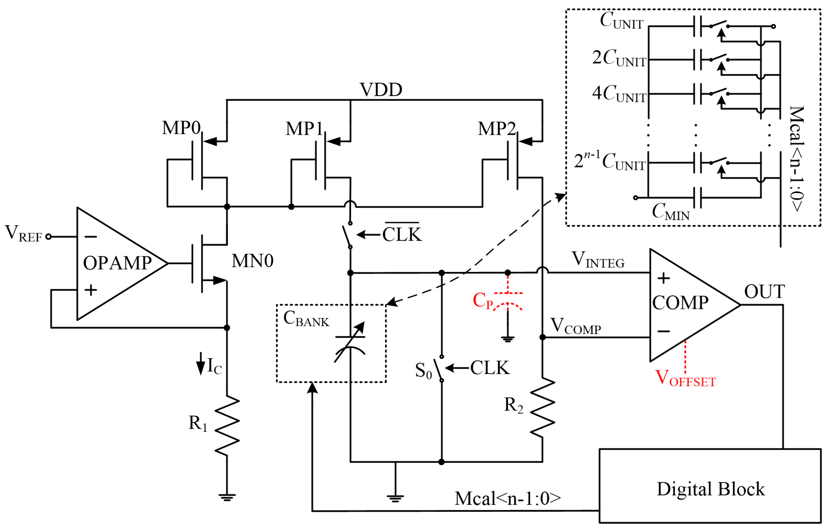
The basic architecture of the proposed tuning scheme is shown in Figure 3. The proposed method utilizes two techniques to minimize the nonidealities discussed above, namely parasitic capacitance cancelation and symmetric comparison, and improve the auto-tuning accuracy:
  • Parasitic capacitance cancelation technique:
As can be seen in Figure 3, two identical capacitor banks are implemented. The redundant CBANK is controlled by a switch S1. A redundant current source MP3 is implemented as well. The digital signal SW1 controls these redundant elements through switches S1 and S2. Firstly, the RC time constant is calibrated with SW1 being 0, which means the redundant elements are not involved in charging VINTEG. The control word ma obtained in the first calibration could satisfy Equation (11):
C M I N + m a C U N I T + C P = I C × 0.5 T V C O M P
where ma is the decimal form of the binary control word Mcal<n-1:0>. Secondly, the time constant is calibrated again with SW1 being 1; the redundant CBANK and MP3 are included in charge node VINTEG. The obtained control word mb could satisfy Equation (12):
2 C M I N + m b C U N I T + C P = 2 I C × 0.5 T V C O M P
By subtracting Equation (11) from Equation (12), the parasitic capacitance CP could be eliminated:
C M I N + 2 m b m a C U N I T = I C × 0.5 T V C O M P
In fact, the target control word mTAGT is supposed to make VINTEG equal VCOMP after being charged for a duration of T⁄2 without CP, so mTAGT should satisfy Equation (14):
C M I N + m T A G T C U N I T = I C × 0.5 T V C O M P
As a result, the value of the target control word mTAGT can be deduced from Equations (13) and (14):
m T A G T = 2 m b m a
which is able to make VINTEG equal VCOMP after being charged for a duration of T 2 without the presence of CP.
2.
Symmetric comparison technique:
As can be seen in Figure 3, three multiplexers controlled by the digital signal SW2 are placed at the input ports and output ports of the comparator, respectively. When SW2 is 0, the multiplexers pass VCOMP to the negative input of the comparator and VINTEG to the positive input. The positive output of the comparator is sampled as OUT. After an auto-tuning procedure, the obtained control word mx could satisfy Equation (16):
C M I N + m x C U N I T = I C × 0.5 T V C O M P + V O F F S E T
When SW2 is 1, the input ports of the comparator are reversed by the multiplexers, as well as the output ports. VCOMP is passed to the positive input of the comparator and VINTEG is passed to the negative input. The negative output of the comparator is sampled as OUT. The control word my obtained in the tuning procedure could satisfy the following equation:
C M I N + m y C U N I T = I C × 0.5 T V C O M P V O F F S E T
As discussed above, the target control word mTAGT satisfies Equation (14), which means the value of mTAGT is higher than mx and lower than my. The mean value of mx and my could be an approximation of mTAGT:
m T A G T m x + m y 2
Note that if VOFFSET is extremely large and is comparable to VCOMP, the accuracy of this strategy can be degraded, but the tuning accuracy is still improved by this strategy. In most cases, the value of VOFFSET is limited and is much lower than VCOMP; therefore, Equation (18) would be a good approximation of mTAGT.
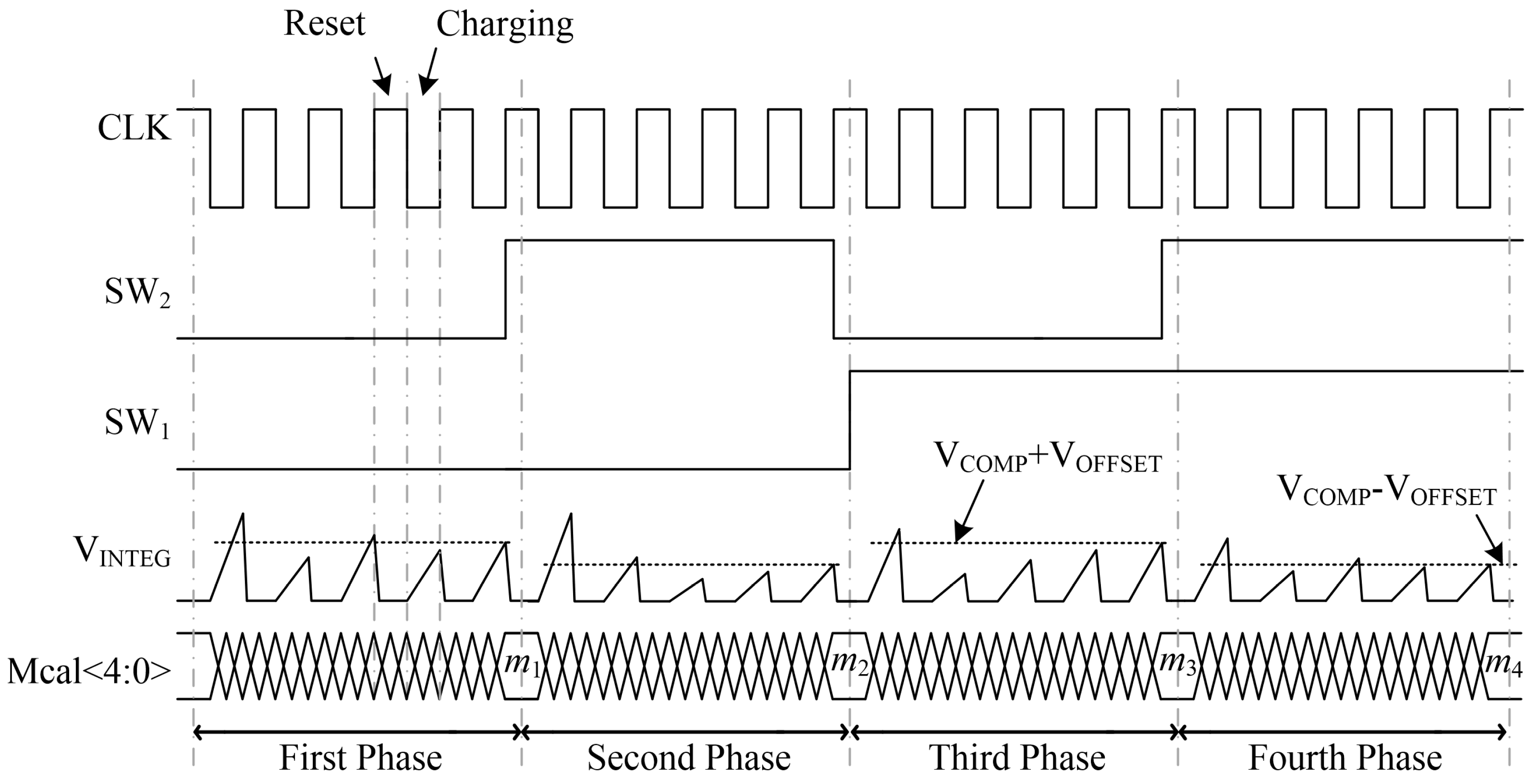
These two techniques are combined to improve the auto-tuning accuracy. As can be seen in Figure 4, the overall auto-tuning process includes four phases, and the time constant is calibrated once in each phase. There are four combinations for the values of SW1 and SW2, which are “0-0”, “0-1”, “1-0” and “1-1”. Each phase adopts one of these combinations. A successive approximation procedure is utilized to accelerate the tuning process. The digital block executes the successive approximation procedure to accelerate the tuning process. The process is described in the following four phases:
  • For the first phase, SW1 and SW2 are both set to 0. The multiplexers pass VCOMP to the negative input of the comparator and VINTEG to the positive input. The positive output of the comparator is sampled as OUT. The redundant CBANK and transistor MP2 are cut off by S1 and S2. The control word is searched by means of the successive approximation procedure. The resultant value of the control word Mcal<4:0> is latched up as m1.
  • For the second phase, SW1 stays 0 and SW2 switches to 1. The input ports of the comparator are reversed by the multiplexers, as well as the output ports. The same calibration procedure is repeated for a second time, and the resultant control word is latched up as m2.
  • For the third phase, SW1 switches to 1 and SW2 switches to 0. In this phase, MP3 and the redundant CBANK take part in charging VINTEG. Two capacitor banks are charged by 2IC at the same node. The connections of the multiplexers are the same as in phase 1. The control word m3 is obtained by a tuning procedure.
  • For the fourth phase, SW1 and SW2 are both 1. VCOMP is passed to the positive input of the comparator and VINTEG is passed to the negative input. The redundant part is involved as in phase 3. The calibration result is m4.
Once m1~m4 are obtained, a final control word can be inferred to avoid the influence of CP and VOFFSET. The final value of the control word mTAGT can be expressed as
m T A G T = ( 2 m 3 m 1 ) + ( 2 m 4 m 2 ) 2 = m 4 + m 3 m 2 + m 1 2
The value of mTAGT is latched up and transferred to the capacitor bank in the slave circuit and the auto-tuning is finished. The master circuit is deactivated to reduce the power consumption and can be reactivated if needed.
Figure 5 illustrates the flow chart of the tuning procedure through successive approximation. Mcal<4:0> is set to “10000” in the beginning. CLK is 1 in the reset phase, the capacitor bank is discharged and VINTEG is set to be 0. The charging mode begins at the negative edge of CLK. CBANK is charged for a duration of T/2. Comparison is then performed between VINTEG and VCOMP, and the comparison result is transferred to the digital block. If VINTEG is higher than VCOMP, which means the present value of CBANK is lower than the nominal value, the output of comparator OUT is high; otherwise, OUT is low. The value of Mcal<4:0> is altered after each comparison. If OUT is high, set the most significant bit of Mcal<4:0> to be 1, otherwise set it to be 0. In both conditions, set the next bit to be 1 for the next reset-charge cycle. For example, if the output of the comparator in the first process is high, set Mcal<4:0> to be “11000” for the second reset-charge process, otherwise set it to be “01000”. Then repeat the reset-charge and comparison process. Move from the most significant bit to the least significant bit and apply the same operation on each bit. The value of Mcal<4:0> is registered after five reset-charge operations. This routine is performed four times under four different combinations of the values of SW1 and SW2. Four binary control words can be obtained, and the final control word is calculated by Equation (19) and transferred to the slave circuit.
The digital control word is sequentially increased or decreased by one least significant bit in the conventional tuning scheme; the longest tuning procedure may take 2n−1 cycles of the reset–charge operation. In this work, only n cycles are needed for the same tuning procedure due to successive approximation. Indeed, as a cost of diminishing nonidealities, both two-way comparing strategy and capacitor bank redundancy will double the tuning time. However, 4n cycles is still less than 2n−1 in applications where the control word is wider than five bits, which is usual when high tuning accuracy or a wide tuning range is demanded. Furthermore, the calibration process can be performed four times or only once according to the actual situation. In less critical applications, it is not necessary to excessively pursue high tuning accuracy; therefore, the calibration process can be performed only once after powering on, reducing the tuning time and the power consumption.

4. Circuit Design and Simulation Results

The proposed tuning circuit was designed under an SMIC 55 nm CMOS process, provided by Semiconductor Manufacturing International Corporation. In order to validate the auto-tuning circuit, a 4th-order low-pass active-RC filter was also designed as the circuit to be tuned.

4.1. Circuit Design

The digital block including SAR logic was realized using hardware description language. Two same capacitor banks with a 5-bit control word were applied in the circuit. The range of both capacitor banks were (50%, 150%) of the nominal capacitance. The comparator in the circuit is a conventional dynamic double-tail comparator, which shows high speed and power efficiency [32]. The 4th-order low-pass active-RC filter was cascaded by two MFB biquads, as shown in Figure 6. The cut-off frequency fc for attenuation of 0.5 dB was designed to be 3 MHz, and the passband gain was 0 dB. The input IP3 was 17 dBm given a typical process corner, room temperature and nominal power supply. The capacitance values of the four different capacitors in the filter are designed as integer multiples of the capacitor bank in the calibration circuit; once the capacitor bank is tuned, the same capacitor banks can be used to form the capacitors in the filter.
Note that the designer should set the value of capacitor banks according to the power, area and tuning accuracy constraints, like in all the master–slave tuning techniques. A larger capacitance value of the capacitor bank will result in a higher tuning accuracy because it is closer to the real capacitance value required in the filter. However, the area and power consumption will be higher. A smaller capacitor bank will make the area and power consumption lower, but more capacitor banks would be used in the slave circuit; nonidealities such as coupling and parasitic capacitances will have a serious impact on the calibration accuracy.
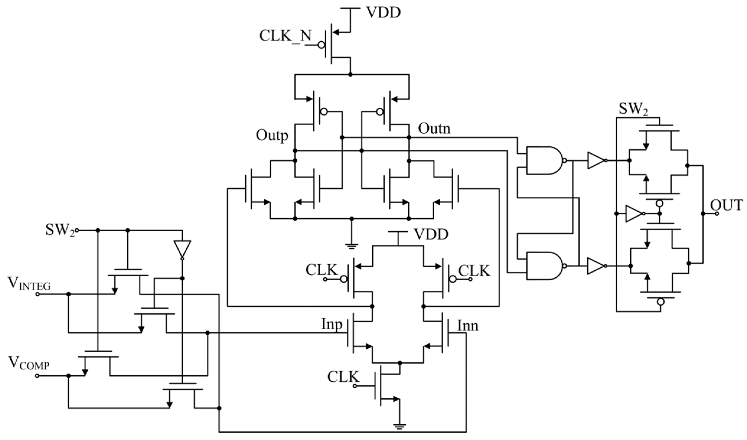
The calibration accuracy could be affected if the output delay of the comparator is high; therefore, a dynamic comparator is adopted to achieve high speed and power efficiency. The comparator accompanied by the multiplexers is shown in Figure 7. This is a classic dynamic double-tail comparator. The output delay time of the dynamic comparator is much shorter than the clock period, leaving a large time margin for output sampling; therefore, the calibration accuracy is not affected. Under the control of a 1-bit signal SW2, the CMOS multiplexers could exchange the connection of two input nodes, helping to minimize the error induced by the DC offset as discussed earlier.

4.2. Simulation Results

Since the offset voltage is caused by random mismatches, the offset voltage of the dynamic comparator was investigated through Monte Carlo simulations. Process variation and mismatch were both considered in the simulations. As a result, input offset voltages up to 60 mV were observed. Therefore, an input offset voltage of 60 mV was applied to the comparator in simulations for illustration.
Post-simulations were carried out under PVT variations to validate the auto-tuning scheme. A voltage source of 60 mV were applied to model the effect of offset voltage. The nominal supply voltage VDD was 1.2 V. Eight corners were considered besides the typical corner. The temperature varied from −40 °C to 125 °C, and the supply voltage varied from 1.1 V to 1.3 V.
The simulated and calculated control words at one of the corners are listed in Table 1 as an example. The process corner was FF, supply voltage was 1.1 V and the temperature was 125 °C. Parasitic capacitance accounts for the difference between the control words obtained in phase 1 and phase 3. The difference between the control words obtained in phase 1 and phase 2 is induced by the offset voltage. As can be seen, the effects of these nonidealities have been minimized by the calculated control word.
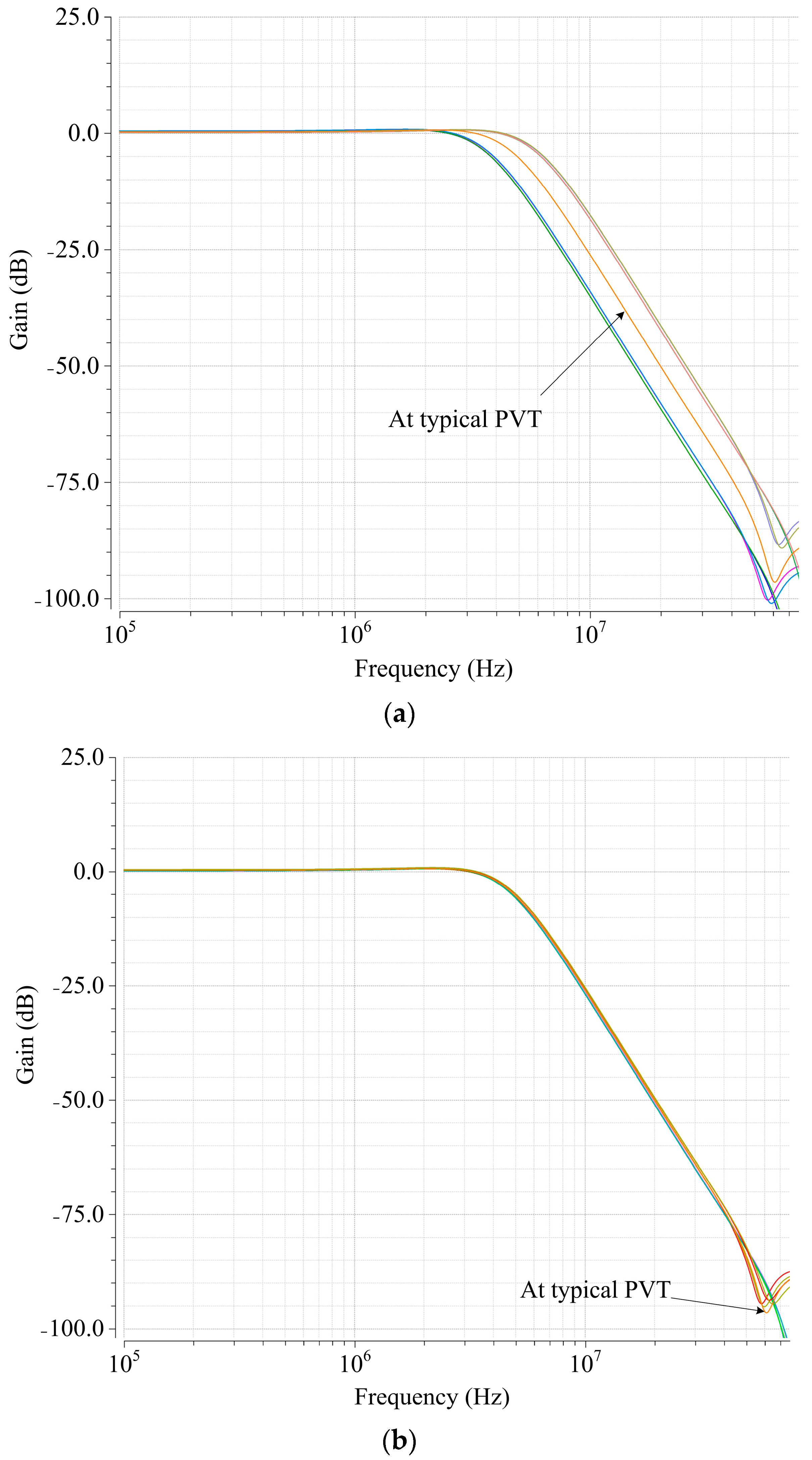
Figure 8 shows the simulated frequency responses in all nine corners of the filter before and after RC time constant calibration. Obvious errors can be observed before the calibration. Table 2 shows the 0.5 dB cut-off frequency fc at nine corners, whose first row indicates the result at a typical corner. The average tuning error was 2.21%, and the tuning error spans from 0.33% to 3.67% which includes the quantization error due to the discrete approach and other non-idealities. The whole tuning process took 3 µs, including sufficient time margin for digital block and general reset. The convergence time of the automatic calibration is determined by the number of bits of the binary control word. For certain bandwidth and resistance value, the capacitor bank can be binarily weighted by more bits or less bits. In other words, the designers need to trade off between convergence time and quantization error.
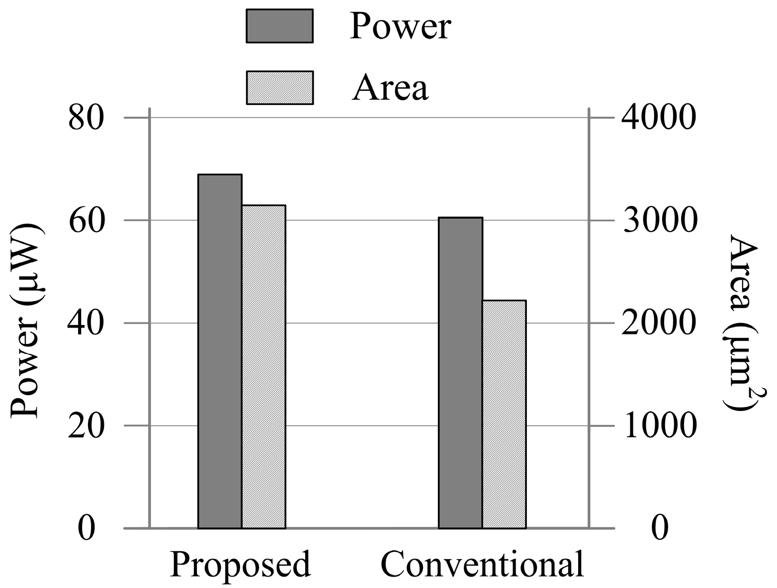
The conventional scheme discussed in Section 2 was also designed for comparison. Figure 9 compares the total circuit area and average power consumption of the tuning schemes. Figure 10 shows the tuning error of the proposed scheme and conventional scheme at different corners. As can be seen, due to the parasitic capacitance and the offset voltage of the comparator, the conventional scheme shows a large tuning error which spans from 12.33% to 15.67%. However, the influences of these nonidealities have been minimized by the proposed scheme. The tradeoffs are that the proposed tuning scheme shows 13.7% higher power and 41% higher area consumption than the conventional scheme. As the tuning circuits are powered off after the tuning process, these tradeoffs are acceptable to applications that are not highly power-sensitive or area-sensitive.

5. Conclusions

The accuracy of the RC time constant is critical for many continuous-time analog circuits. This paper reports a high-accuracy on-chip auto-tuning scheme to calibrate the RC time constant of integrated continuous-time filters. Two techniques are introduced to improve the tuning accuracy, namely the parasitic capacitance cancelation technique and the symmetric comparison technique. The tuning scheme is validated in 55 nm CMOS technology. Results show that the tuning error induced by parasitic capacitance and the DC offset can be reduced. The scheme is suitable for continuous-time systems where high tuning accuracy is demanded.

Author Contributions

Conceptualization, G.J. and L.Z.; methodology, G.J.; software, G.J. and H.W.; validation, H.W. and Y.Y.; resources, G.J. and Y.Z.; writing—original draft preparation, G.J.; writing—review and editing, G.J. and H.W.; supervision, G.J.; project administration, G.J.; funding acquisition, G.J. All authors have read and agreed to the published version of the manuscript.

Funding

This study was funded by the Special Fund for Research on National Major Research Instruments of the National Natural Science Foundation of China (NSFC) (Grant number: 82327810), and the Key Research and Development Projects of Shaanxi Province (Grant number: 2020GY-080).

Data Availability Statement

Data are contained within the article.

Acknowledgments

The authors wish to thank the anonymous reviewers for their work.

Conflicts of Interest

Lei Zheng is an employee of Guangzhou Quanshengwei Information Technology Co., Ltd. The paper reflects the views of the scientists, not the company. The remaining authors declare no conflicts of interest.

References

  1. Lavalle-Aviles, F.; Sánchez-Sinencio, E. A 0.6-V Power-Efficient Active-RC Analog Low-Pass Filter with Cutoff Frequency Selection. IEEE Trans. Very Large Scale Integr. (VLSI) Syst. 2020, 28, 1757–1769. [Google Scholar] [CrossRef]
  2. Rasekh, A.; Bakhtiar, M.S. Design of Low-Power Low-Area Tunable Active RC Filters. IEEE Trans. Circuits Syst. II: Express Briefs 2018, 65, 6–10. [Google Scholar] [CrossRef]
  3. Gao, S.; Chen, Z.-J.; Sun, X.; Yang, S.; Li, B.; Lin, X.-L. A Reconfigurable Active-RC Filter with Variable Gain and an RC-Reused Tuning Circuit. In Proceedings of the 2022 IEEE Asia Pacific Conference on Circuits and Systems (APCCAS), Shenzhen, China, 11–13 November 2022. [Google Scholar]
  4. Compassi-Severo, L.; Noije, W.V. A 0.4-V 10.9-μW/Pole Third-Order Complex BPF for Low Energy RF Receivers. IEEE Trans. Circuits Syst. I Regul. Pap. 2019, 66, 2017–2026. [Google Scholar] [CrossRef]
  5. Sanabria-Borbón, A.C.; Sánchez-Sinencio, E. Synthesis of High-Order Continuously Tunable Low-Pass Active-R Filters. IEEE Trans. Circuits Syst. I Regul. Pap. 2021, 68, 1841–1854. [Google Scholar] [CrossRef]
  6. Miti, D.; Jovanovi, G.; Stojev, M.; Anti, D. Fast Locking Time Biquadratic Band-Pass Filter Utilizing Nonlinear Sliding-Mode Controller. J. Circuits Syst. Comput. 2021, 30, 2150154. [Google Scholar] [CrossRef]
  7. Kledrowetz, V.; Haze, J.; Prokop, R.; Fujcik, L. An Active Resistor with a Lower Sensitivity to Process Variations, and its Application in Current Reference. IEEE Access 2020, 8, 197263–197275. [Google Scholar] [CrossRef]
  8. Zhang, C.; Shang, L.; Wang, Y.; Tang, L. A CMOS Programmable Fourth-Order Butterworth Active-RC Low-Pass Filter. Electronics 2020, 9, 204. [Google Scholar] [CrossRef]
  9. Osman, H.; Life, E.S.-S. A PVT-Resilient, Highly-Linear Fifth-Order Ring-Oscillator-Based Filter. IEEE Trans. Circuits Syst. I Regul. Pap. 2020, 67, 4295–4308. [Google Scholar] [CrossRef]
  10. Karolis, K.; Romualdas, N. A method for continuous tuning of MOSFET–RC filters with extended control range. J. Electr. Eng. 2016, 67, 449–453. [Google Scholar]
  11. Kumar, V.; Mehra, R.; Islam, A. A 2.5 GHz Low Power, High-Q, Reliable Design of Active Bandpass Filter. IEEE Trans. Device Mater. Reliab. 2017, 17, 229–244. [Google Scholar] [CrossRef]
  12. Gao, T.; Li, W.; Chen, Y.; Li, N.; Ren, J. A 5.5mW 80-400MHz Gm-C low pass filter with a unique auto-tuning system. IEICE Electron. Express 2011, 8, 1034–1039. [Google Scholar] [CrossRef]
  13. Abdolmaleki, M.; Dousti, M.; Tavakoli, M.B. Design and simulation of tunable low-pass Gm-C filter with 1 GHz cutoff frequency based on CMOS inventers for high speed telecommunication applications. Analog. Integr. Circuits Signal Process. 2019, 100, 279–286. [Google Scholar] [CrossRef]
  14. Abdolmaleki, M.; Dousti, M.; Tavakoli, M.B. Design and simulation of fourth order low-pass Gm-C filter with novel auto-tuning circuit in 90 nm CMOS. Analog. Integr. Circuits Signal Process. 2021, 107, 451–461. [Google Scholar] [CrossRef]
  15. Xia, B.; Yan, S.; Sanchez-Sinencio, E. An RC time constant auto-tuning structure for high linearity continuous-time /spl Sigma//spl Delta/ modulators and active filters. IEEE Trans. Circuits Syst. I Regul. Pap. 2004, 51, 2179–2188. [Google Scholar] [CrossRef]
  16. Huang, H.Y.; Wu, C.C.; Luo, C.H. An MICS band frequency synthesizer using active inductor and auto-calibration scheme. Int. Microelectron. J. 2021, 43, 592–599. [Google Scholar] [CrossRef]
  17. Chen, Z.; Wu, Q.; Shi, C.; Zhang, R. A 1.2 GHz bandwidth and 88 dB gain range analog baseband for multi-standard 60 GHz applications. IEICE Electron. Express 2022, 17, 20190742. [Google Scholar] [CrossRef]
  18. Jin, B.; Chen, Z.; Liu, X.; Shen, Z.; Bao, Y.; Xing, Y.; Wan, P. A SAR-based Fast Automatic Frequency Tuning Circuit in a 3-th Order Active-RC Complex Filter. In Proceedings of the 2021 IEEE 15th International Conference on Anti-counterfeiting, Security, and Identification (ASID), Xiamen, China, 29–31 October 2021. [Google Scholar]
  19. Guo, Y.; Jin, J.; Liu, X.; Zhou, J. An Inverter-Based Continuous Time Sigma Delta ADC with Latency-Free DAC Calibration. IEEE Trans. Circuits Syst. I Regul. Pap. 2020, 67, 3630–3642. [Google Scholar] [CrossRef]
  20. Lee, S.; Shi, C.; Wang, J.; Sanabria, A.; Osman, H.; Hu, J.; Sanchez-Sinencio, E.A. Built-In Self-Test and In Situ Analog Circuit Optimization Platform. IEEE Trans. Circuits Syst. I Regul. Pap. 2018, 65, 3445–3458. [Google Scholar] [CrossRef]
  21. Talebzadeh, J.; Kale, I. A novel two-channel continuous-time time-interleaved 3rd-order sigma-delta modulator with integrator-sharing topology. Analog. Integr. Circuits Signal Process 2018, 95, 375–385. [Google Scholar] [CrossRef]
  22. Ju, C.; Li, X.; Zou, J.; Wei, Q.; Zhou, B.; Zhang, R. An Auto-Tuning Continuous-Time Bandpass Sigma-Delta Modulator with Signal Observation for MEMS Gyroscope Readout Systems. Sensors 2020, 20, 1973. [Google Scholar] [CrossRef]
  23. Hughes, J.B.; Bird, N.C.; Soin, R.S. Self-tuned RC-active filters for VLSI. Electron. Lett. 1986, 22, 993–994. [Google Scholar] [CrossRef]
  24. Cunha, M.W.L.; Schneider, M.C.; Dalcastagne, A.L. Automatic tuning of MOSFET-C filters using digitally programmable current attenuators. In Proceedings of the 1997 IEEE International Symposium on Circuits and Systems (ISCAS), Hong Kong, China, 12 June 1997. [Google Scholar]
  25. Oshima, T.; Maio, K.; Hioe, W.; Hioe, W.; Shibahara, Y. Novel automatic tuning method of RC filters using a digital-DLL technique. IEEE J. Solid-State Circuits 2004, 39, 2052–2054. [Google Scholar] [CrossRef]
  26. Kiela, K.; Jurgo, M.; Macaitis, V.; Macaitis, V.; Navickas, R. Wideband Reconfigurable Integrated Low-Pass Filter for 5G Compatible Software Defined Radio Solutions. Electronics 2021, 10, 734. [Google Scholar] [CrossRef]
  27. Wang, R.; Lin, M.; Wang, H.; Sun, S. A widely tunable active-RC complex filter for multi-mode wireless receivers with automatic frequency tuning. IEICE Electron. Express 2016, 13, 20160764. [Google Scholar] [CrossRef]
  28. Kladovščikov, L.; Navickas, R.; Kiela, K. Self-tuning system for multistandard active RC filters. Microelectron. J. 2019, 90, 260–266. [Google Scholar] [CrossRef]
  29. Omeni, O.; Rodriguez-Villegas, E.; Toumazou, C. A Micropower CMOS Continuous-Time Filter with On-Chip Automatic Tuning. Int. IEEE Trans. Circuits Syst. I Regul. Pap. 2005, 52, 695–705. [Google Scholar] [CrossRef]
  30. Gandhi, P.P.; Devashrayee, N.M. A novel low offset low power CMOS dynamic comparator. Analog. Integr. Circuits Signal Process. 2018, 96, 147–158. [Google Scholar] [CrossRef]
  31. Kladovšcikov, L.; Navickas, R. Review of self tuning methods for direct conversion transceivers. In Proceedings of the 2017 Open Conference of Electrical, Electronic and Information Sciences, Vilnius, Lithuania, 27 April 2017. [Google Scholar]
  32. Zhang, M.; Fan, X. An energy-efficient SAR ADC using a single-phase clocked dynamic comparator with energy and speed enhanced technique. IEICE Electron. Express 2017, 14, 20170219. [Google Scholar] [CrossRef]
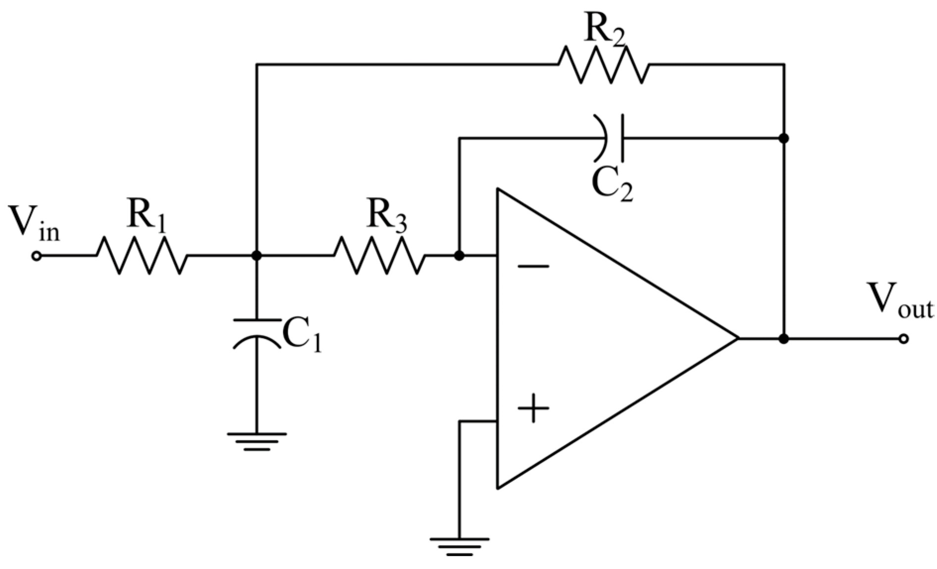
Figure 1. MFB low-pass biquad.
Micromachines 15 00166 g001
Figure 2. The conventional master–slave tuning scheme.
Micromachines 15 00166 g002
Figure 3. The proposed master–slave scheme.
Micromachines 15 00166 g003
Figure 4. Transient waveforms of the proposed tuning circuit.
Micromachines 15 00166 g004
Figure 5. Flow chart of the four-phase tuning procedure.
Micromachines 15 00166 g005
Figure 6. The 4th-order low-pass active-RC filter.
Micromachines 15 00166 g006
Figure 7. Comparator circuit.
Micromachines 15 00166 g007
Figure 8. Simulated frequency response of the filter under PVT variations (a) before calibration and (b) after calibration.
Micromachines 15 00166 g008
Figure 9. Circuit area and power consumption of the tuning circuits.
Micromachines 15 00166 g009
Figure 10. Tuning error at different corners.
Micromachines 15 00166 g010
Table 1. Digital control words in the tuning process under a process corner of FF, supply voltage of 1.1 V and temperature of 125 °C.
Digital Control WordValue
m1 obtained in phase 110010
m2 obtained in phase 210011
m3 obtained in phase 310111
m4 obtained in phase 111000
Calculated mTAGT11101
Table 2. The cut-off frequency under PVT variations.
CornersProcess CornerVoltage (V)Temperature (°C)fc before Calibration (MHz)fc after Calibration (MHz)Tuning Error
Typical CornerTT1.2273.00--
Corner 1FF1.1−404.003.103.33%
Corner 2FF1.11253.983.020.67%
Corner 3FF1.3−403.952.971.00%
Corner 4FF1.31253.972.913.00%
Corner 5SS1.1−402.272.990.33%
Corner 6SS1.11252.272.903.33%
Corner 7SS1.3−402.262.932.33%
Corner 8SS1.31252.252.893.67%
Disclaimer/Publisher’s Note: The statements, opinions and data contained in all publications are solely those of the individual author(s) and contributor(s) and not of MDPI and/or the editor(s). MDPI and/or the editor(s) disclaim responsibility for any injury to people or property resulting from any ideas, methods, instructions or products referred to in the content.