
Capacitance–Voltage Fluctuation of SixNy-Based Metal–Insulator–Metal Capacitor Due to Silane Surface Treatment


Abstract
1. Introduction
2. Materials and Methods
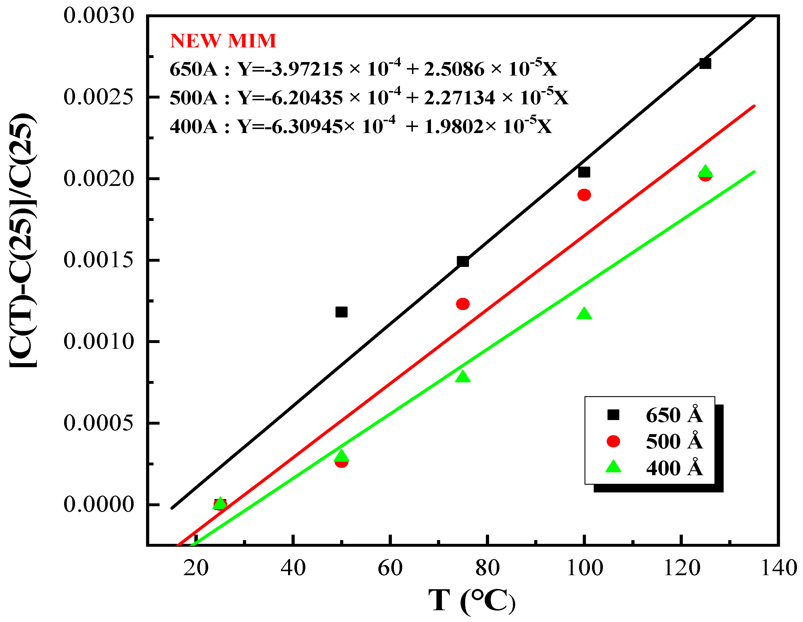
3. Results and Discussion
4. Conclusions
Author Contributions
Funding
Data Availability Statement
Acknowledgments
Conflicts of Interest
References
- Xiong, L.; Hu, J.; Yang, Z.; Li, X.; Zhang, H.; Zhang, G. Dielectric Properties Investigation of Metal–Insulator–Metal (MIM) Capacitors. Molecules 2022, 27, 3951. [Google Scholar] [CrossRef] [PubMed]
- Karthik, R.; Manjusha, K.A. Metal Insulator Metal Capacitors-State of the Art. J. Comput. Theor. Nanosci. 2018, 15, 2346–2349. [Google Scholar] [CrossRef]
- Ding, S.-J.; Hu, H.; Zhu, C.; Kim, S.J.; Yu, X.; Li, M.-F.; Cho, B.J.; Chan, D.S.H.; Yu, M.B.; Rustagi, S.C.; et al. RF, DC, and reliability characteristics of ALD HfO2-Al2O3 laminate MIM capacitors for Si RF IC applications. IEEE Trans. Electron Devices 2004, 51, 886–894. [Google Scholar] [CrossRef]
- Choi, E.; Kim, A.; Kwon, S.H.; Pyo, S.G. Effect of Interface Treatment on the Voltage Linearity in 8 fF/μm2 High-k Dielectric and Combination Stacks on Metal Insulator Metal (MIM) Capacitor. Sci. Adv. Mater. 2018, 10, 467–470. [Google Scholar] [CrossRef]
- Hoa, P.T. High-K Dielectrics in Metal Insulator Metal (MIM) Capacitors for RF Applications. Ph.D. Thesis, National University of Singapore, Singapore, 2011. [Google Scholar]
- Pavunny, S.P.; Misra, P.; Scott, J.F.; Katiyar, R.S. Advanced high-k dielectric amorphous LaGdO3 based high density metal-insulator-metal capacitors with sub-nanometer capacitance equivalent thickness. Appl. Phys. Lett. 2013, 102, 252905. [Google Scholar] [CrossRef]
- Ding, S.-J.; Hu, H.; Lim, H.; Kim, S.; Yu, X.; Zhu, C.; Li, M.; Cho, B.J.; Chan, D.S.; Rustagi, S.C. High-performance MIM capacitor using ALD high-k HfO2-Al2O3 laminate dielectrics. IEEE Electron Device Lett. 2003, 24, 730–732. [Google Scholar] [CrossRef]
- Sul, W.S.; Pyo, S.G. RF Characteristic Analysis Model Extraction on the Stacked Metal–Insulator–Metal Capacitors for Radio Frequency Applications. IEEE Trans. Electron Devices 2014, 61, 3011–3013. [Google Scholar] [CrossRef]
- Mu, J.; Chou, X.; Ma, Z.; He, J.; Xiong, J. High-Performance MIM Capacitors for a Secondary Power Supply Application. Micromachines 2018, 9, 69. [Google Scholar] [CrossRef]
- Li, W.; Lu, X.; Yang, R.; Liang, F.; Chen, W.; Xie, Z.; Zheng, J.; Zhu, J.; Huang, Y.; Yue, W.; et al. Highly sensitive and reproducible SERS substrates with binary colloidal crystals (bCCs) based on MIM structures. Appl. Surf. Sci. 2022, 597, 153654. [Google Scholar] [CrossRef]
- Jeon, S.; Sung, S.-K.; Jang, E.-H.; Jeong, J.; Surabhi, S.; Choi, J.-H.; Jeong, J.-R. Multilayer metal-oxide-metal nanopatterns via nanoimprint and strip-off for multispectral resonance. Appl. Surf. Sci. 2018, 428, 280–288. [Google Scholar] [CrossRef]
- Smitha, P.S.; Babu, V.S.; Shiny, G. Critical parameters of high performance metal-insulator-metal nanocapacitors: A review. Mater. Res. Express 2019, 6, 122003. [Google Scholar] [CrossRef]
- Sejas-García, S.C.; Torres-Torres, R.; Valderrama-B, R.; Molina, J. Complex Permittivity Determination of Thin-Films through RF-Measurements of a MIM Capacitor. IEEE Microw. Wirel. Compon. Lett. 2014, 24, 805–807. [Google Scholar] [CrossRef]
- Nam, M.; Kim, A.; Kang, K.; Choi, E.; Kwon, S.H.; Lee, S.J.; Pyo, S.G. Characterization of atomic layer deposited Al2O3/HfO2 and Ta2O5/Al2O3 combination stacks. Sci. Adv. Mater. 2016, 8, 1958–1962. [Google Scholar] [CrossRef]
- Jin Chung, J.; Hyuk Kim, T.; Ahsan Saeed, M.; Won Shim, J. Laminated indium-oxide/molybdenum-oxide nanocomposites for high-work-function electrodes in organic photovoltaics and capacitor devices. Appl. Surf. Sci. 2023, 610, 155526. [Google Scholar] [CrossRef]
- Guo, Y.; Wang, S.; Du, X.; Liang, S.; Huang, S.; Peng, S.; Xie, Y.; Ma, M.; Xiong, L. Construction of ultrahigh capacity density carbon nanotube based MIM capacitor. Energy Storage Mater. 2023, 63, 103064. [Google Scholar] [CrossRef]
- Ruhl, G.; Lehnert, W.; Lukosius, M.; Wenger, C.; Baristiran Kaynak, C.; Blomberg, T.; Haukka, S.; Baumann, P.K.; Besling, W.; Roest, A.; et al. Dielectric Material Options for Integrated Capacitors. ECS J. Solid State Sci. Technol. 2014, 3, N120–N125. [Google Scholar] [CrossRef]
- Zheng, G.; He, Y.L.; Zhu, B.; Wu, X.; Zhang, D.W.; Ding, S.J. Improvement of Voltage Linearity and Leakage Current of MIM Capacitors With Atomic Layer Deposited Ti-Doped ZrO2 Insulators. IEEE Trans. Electron Devices 2023, 70, 3064–3070. [Google Scholar] [CrossRef]
- Park, Y.S.; Cho, S.-J.; Boo, J.-H.; Hong, B. Surface and electrical properties of organic–inorganic hybrid structure as gate insulator to organic thin film transistor. Appl. Surf. Sci. 2009, 256, 1023–1027. [Google Scholar] [CrossRef]
- Wu, Y.-H.; Kao, C.-K.; Chen, B.-Y.; Lin, Y.-S.; Li, M.-Y.; Wu, H.-C. High density metal-insulator-metal capacitor based on ZrO2/Al2O3/ZrO2 laminate dielectric. Appl. Phys. Lett. 2008, 93, 033511. [Google Scholar] [CrossRef]
- Xu, T.; Tekes, C.; Degertekin, F.L. CMUTs with high-K atomic layer deposition dielectric material insulation layer. IEEE Trans. Ultrason. Ferroelectr. Freq. Control. 2014, 61, 2121–2131. [Google Scholar] [CrossRef]
- Sudheendran, K.; Pamu, D.; Ghanashyam Krishna, M.; James Raju, K.C. Determination of dielectric constant and loss of high-K thin films in the microwave frequencies. Measurement 2010, 43, 556–562. [Google Scholar] [CrossRef]
- Holden, K.E.K.; Hall, G.D.R.; Cook, M.; Kendrick, C.; Pabst, K.; Greenwood, B.; Daugherty, R.; Gambino, J.P.; Allman, D.D.J. Dielectric Relaxation, Aging and Recovery in High-K MIM Capacitors. In Proceedings of the 2021 IEEE International Reliability Physics Symposium (IRPS), Monterey, CA, USA, 21–25 March 2021; pp. 1–10. [Google Scholar]
- Zhao, C.; Zhao, C.Z.; Werner, M.; Taylor, S.; Chalker, P. Dielectric relaxation of high-k oxides. Nanoscale Res. Lett. 2013, 8, 456. [Google Scholar] [CrossRef]
- Ohshima, I.; Cheng, W.; Ono, Y.; Higuchi, M.; Hirayama, M.; Teramoto, A.; Sugawa, S.; Ohmi, T. Reliability of silicon nitride gate dielectrics grown at 400 °C formed by microwave-excited high-density plasma. Appl. Surf. Sci. 2003, 216, 246–251. [Google Scholar] [CrossRef]
- Ma, T.P. Gate dielectric properties of silicon nitride films formed by jet vapor deposition. Appl. Surf. Sci. 1997, 117–118, 259–267. [Google Scholar] [CrossRef]
- Yu, H.Y.; Li, M.F.; Kwong, D.L. ALD (HfO2)x(Al2O3)1−x high-k gate dielectrics for advanced MOS devices application. Thin Solid Films 2004, 462–463, 110–113. [Google Scholar] [CrossRef]
- Lue, H.T.; Lai, S.C.; Hsu, T.H.; Du, P.Y.; Wang, S.Y.; Hsieh, K.Y.; Liu, R.; Lu, C.Y. Understanding barrier engineered charge-trapping NAND flash devices with and without high-K dielectric. In Proceedings of the 2009 IEEE International Reliability Physics Symposium, Montreal, QC, Canada, 26–30 April 2009; pp. 874–882. [Google Scholar]
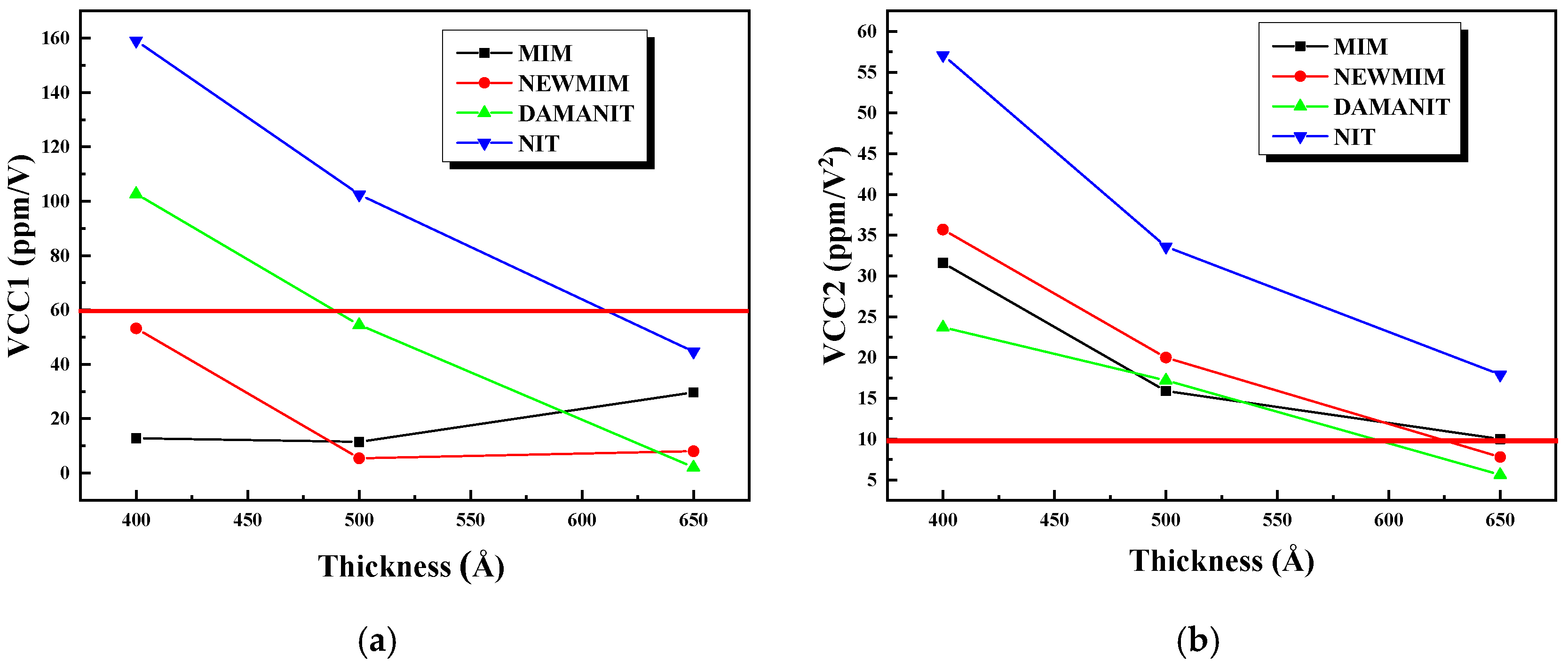
- Cockbain, A.G.; Harrop, P.J. The temperature coefficient of capacitance. J. Phys. D Appl. Phys. 1968, 1, 1109. [Google Scholar] [CrossRef]
- Khaldi, O.; Jomni, F.; Gonon, P.; Mannequin, C.; Yangui, B. Investigation of electrical properties of HfO2 metal–insulator–metal (MIM) devices. Appl. Phys. A 2014, 116, 1647–1653. [Google Scholar] [CrossRef]
- Lee, A.J.; Kim, B.S.; Hwang, J.H.; Kim, Y.; Oh, H.; Park, Y.; Jeon, W. Controlling the crystallinity of HfO2 thin film using the surface energy-driven phase stabilization and template effect. Appl. Surf. Sci. 2022, 590, 153082. [Google Scholar] [CrossRef]
- Li, H.; Yun, H.; Liang, W.; Dong, A.; Miao, M.; Sundaram, K.B. Characterization of Dielectric Breakdown and Lifetime Analysis for Silicon Nitride Metal-Insulator-Metal Capacitors under Electrostatic Discharge Stresses. In Proceedings of the 2018 IEEE International Symposium on the Physical and Failure Analysis of Integrated Circuits (IPFA), Singapore, 16–19 July 2018; pp. 1–5. [Google Scholar]
- Kim, K.H.; Kim, K.S.; Ji, Y.J.; Kang, J.E.; Yeom, G.Y. Silicon nitride deposited by laser assisted plasma enhanced chemical vapor deposition for next generation organic electronic devices. Appl. Surf. Sci. 2021, 541, 148313. [Google Scholar] [CrossRef]
- Yota, J. Effects of Deposition Method of PECVD Silicon Nitride as MIM Capacitor Dielectric for GaAs HBT Technology. ECS Trans. 2011, 35, 229. [Google Scholar] [CrossRef]
- Iversen, C.-R. A high density MIM capacitor in a standard CMOS process. JSTS J. Semicond. Technol. Sci. 2001, 1, 189–192. [Google Scholar]
- Bertaud, T.; Bermond, C.; Blonkowski, S.; Vallee, C.; Lacrevaz, T.; Farcy, A.; Gros-Jean, M.; Flechet, B. Electrical Characterization of Advanced MIM Capacitors With ZrO2 Insulator for High-Density Packaging and RF Applications. IEEE Trans. Compon. Packag. Manuf. Technol. 2012, 2, 502–509. [Google Scholar] [CrossRef]
- Sharp, K.A.; Honig, B. Electrostatic Interactions in Macromolecules: Theory and Applications. Annu. Rev. Biophys. 1990, 19, 301–332. [Google Scholar] [CrossRef]
- Kittel, C. Introduction to Solid State Physics; Wiley: Hoboken, NJ, USA, 2004. [Google Scholar]
- Kim, S.J.; Cho, B.J.; Li, M.-F.; Ding, S.-J.; Zhu, C.; Yu, M.B.; Narayanan, B.; Chin, A.; Kwong, D.-L. Improvement of voltage linearity in high-/spl kappa/ MIM capacitors using HfO2-SiO2 stacked dielectric. IEEE Electron Device Lett. 2004, 25, 538–540. [Google Scholar] [CrossRef]


| (a) | MIM | NEW MIM 650 | DAMA NIT | NIT |
| Dep. rate | ~149 Å/s | ~29 Å/s | ~59 Å/s | 88 Å/s |
| Within W/F unit (1σ) | 1.14% | 1.90% | 2.34% | 2.77% |
| W/F to W/F unit (1σ) | 1.58% | 2.21% | 1.05% | 2.30% |
| Stress | −2.23 × 10⁹ | −1.75 × 10¹⁰ | −2.34 × 10⁹ | |
| H content (N-H: Si-H) | 12.7%: 8.5% | 22.5%: 0.8% | 10.5%: 7.3% | 4.4%: 14.8% |
| N content (N-H/Si-H) | 1.49 | 28.1 | 1.43 | 0.30 |
| (b) | MIM 650 | NEW MIM 650 | DAMA NIT | NIT 650 |
| Step end control | By time | By time | By time | By time |
| Maximum step time | 4.4 s | 22.8 s | 11.0 s | |
| Endpoint selection | No endpoint | No endpoint | No endpoint | No endpoint |
| Pressure | Servo 4.25 Torr | Servo 4.25 Torr | Servo 4.2 Torr | Servo 4.5 Torr |
| RF power | 690 W | 690 W | 420 W | 425 W |
| Susc. temperature | 400 °C | 400 °C | 400 °C | 400 °C |
| Susceptor spacing | 620 mils | 620 mils | 550 mils | 475 mils |
| N2 | 3800 sccm | 3800 sccm | 2500 sccm | 4000 sccm |
| NH3 | 130 sccm | 50 sccm | 38 sccm | 60 sccm |
| SiH4 | 260 sccm | 100 sccm | 110 sccm | 170 sccm |
| Parameter | Setting |
|---|---|
| Display mode | Cp (parallel capacitor), D (dissipation factor) |
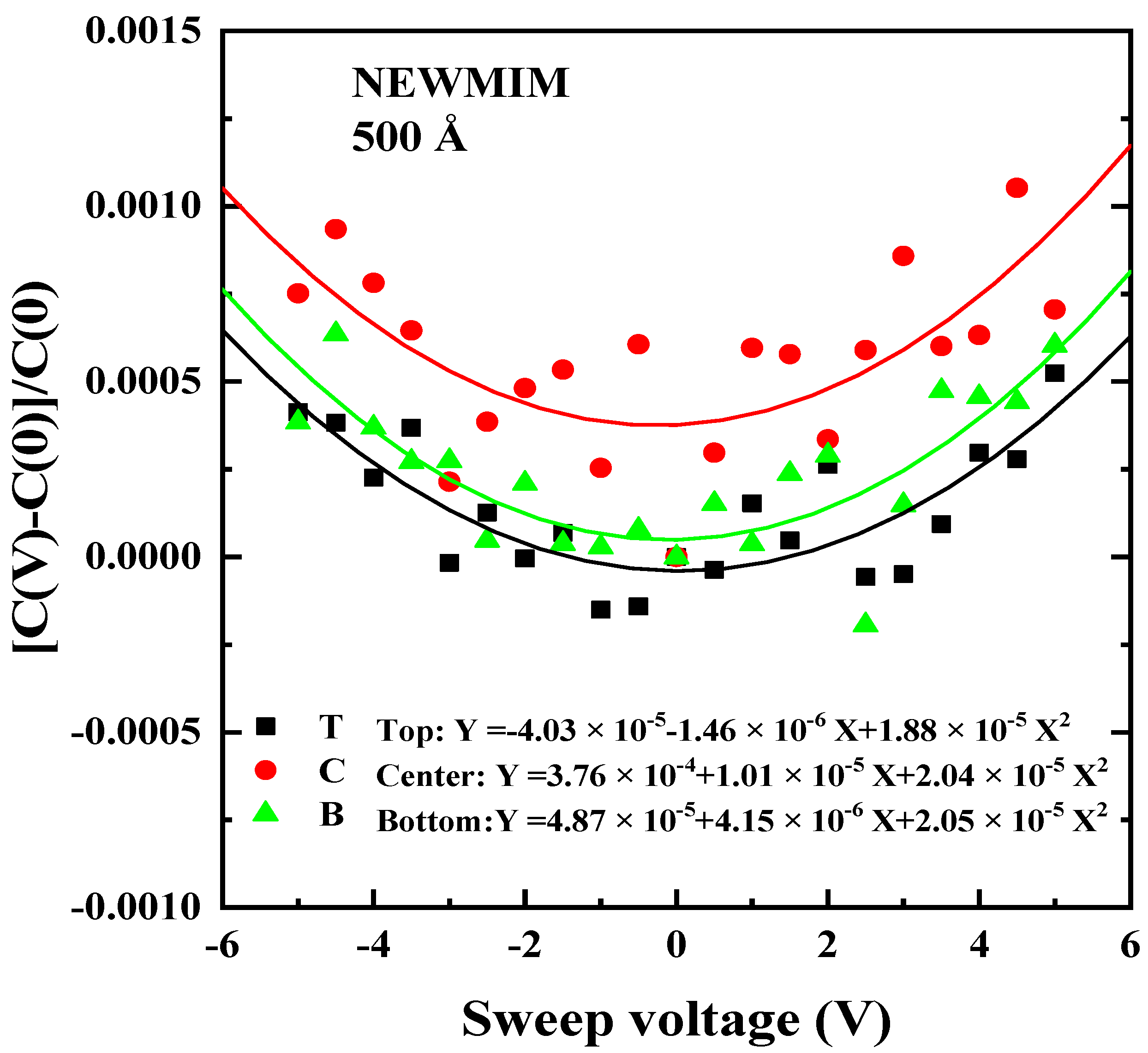
| Sweep voltage (V) | −5~5 |
| Step (V) | 0.5 |
| Oscillation | 0.025 |
| Frequency (kHz) | 100 |
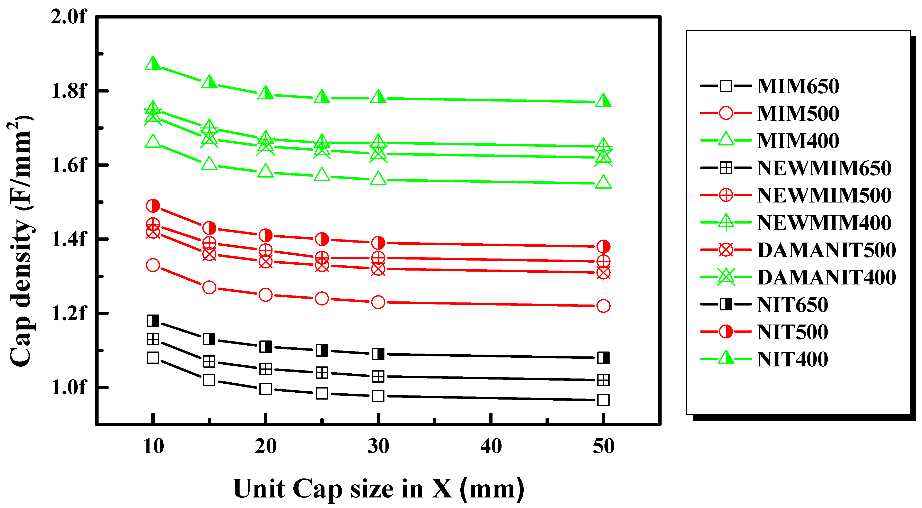
| Capacitor size (μm2) | 10 × 10, 15 × 15, 20 × 20, 25 × 25, 30 × 30, 50 × 50 |
| Measurement points | Three points (top, center, and bottom) |
| Temperature (°C) | 25, 50, 75, 100, 125 |
| Deposition Condition | MIM | NEWMIM | DAMANIT | NIT |
|---|---|---|---|---|
| CD (fF/μm2) | 1.3256 | 1.3203 | 1.3103 | 1.3606 |
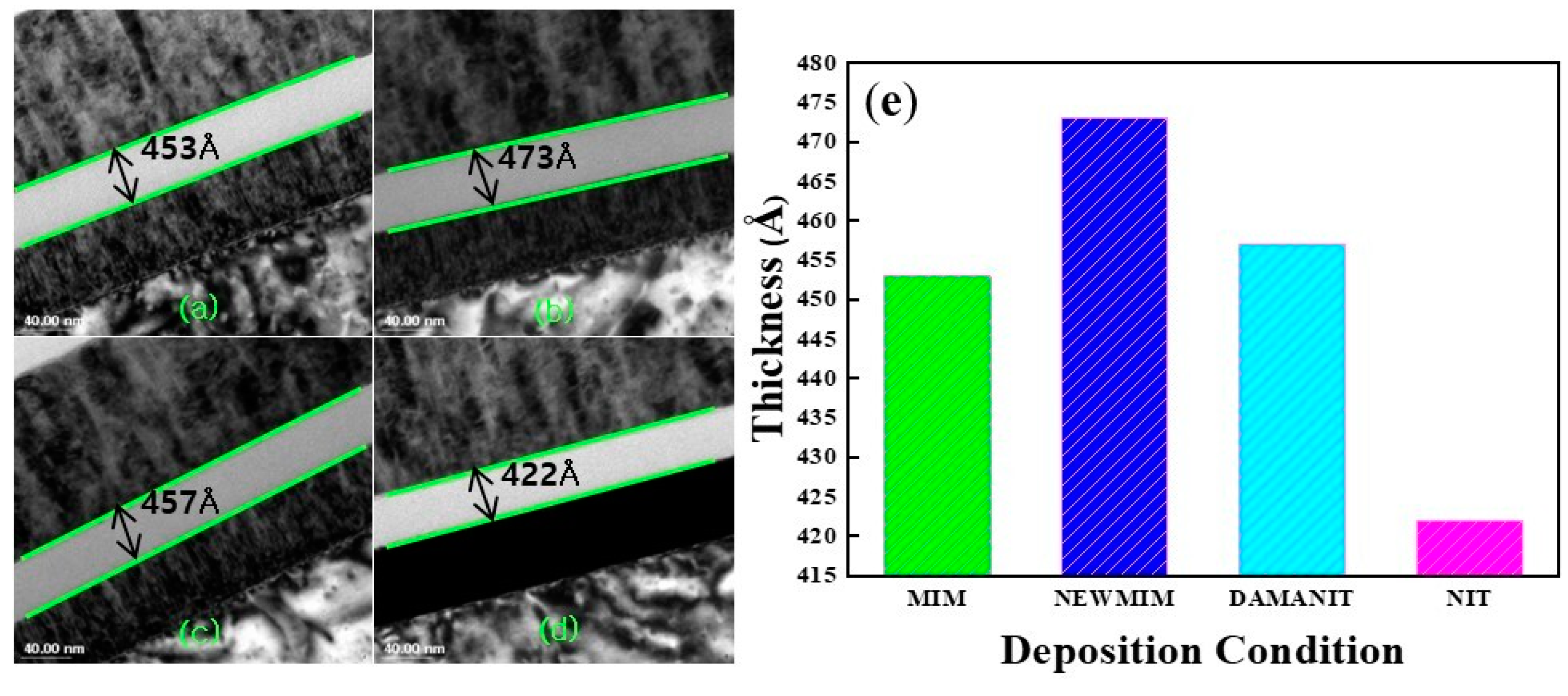
| Thickness (TEM, Å) | 453 | 473 | 457 | 422 |
| k-value (ε0·ε) | 6.00 × 10⁻¹⁷ | 6.25 × 10⁻¹⁷ | 5.99 × 10⁻¹⁷ | 5.74 × 10⁻¹⁷ |
| MIM 650 DEP | NEW MIM 650 DEP | DAMA NIT 650 DEP | NIT 650 DEP | |
|---|---|---|---|---|
| Deposition rate (Å/s) | ~149 | ~29 | ~59 | 88 |
| Within W/F unit (1σ, %) | 1.14 | 1.90 | 2.34 | 2.77 |
| W/F to W/F unit (1σ, %) | 1.58 | 2.21 | 1.05 | 2.30 |
| Stress | −2.23 × 10⁹ | −1.75 × 10¹⁰ | −2.34 × 10⁹ | - |
| H content (N-H:Si-H) | 12.7%:8.5% | 22.5%:0.8% | 10.5%:7.3% | 4.4%:14.8% |
Disclaimer/Publisher’s Note: The statements, opinions and data contained in all publications are solely those of the individual author(s) and contributor(s) and not of MDPI and/or the editor(s). MDPI and/or the editor(s) disclaim responsibility for any injury to people or property resulting from any ideas, methods, instructions or products referred to in the content. |
© 2024 by the authors. Licensee MDPI, Basel, Switzerland. This article is an open access article distributed under the terms and conditions of the Creative Commons Attribution (CC BY) license (https://creativecommons.org/licenses/by/4.0/).
Share and Cite
Choi, T.-M.; Jung, E.-S.; Yoo, J.-U.; Lee, H.-R.; Pyo, S.-G. Capacitance–Voltage Fluctuation of SixNy-Based Metal–Insulator–Metal Capacitor Due to Silane Surface Treatment. Micromachines 2024, 15, 1204. https://doi.org/10.3390/mi15101204
Choi T-M, Jung E-S, Yoo J-U, Lee H-R, Pyo S-G. Capacitance–Voltage Fluctuation of SixNy-Based Metal–Insulator–Metal Capacitor Due to Silane Surface Treatment. Micromachines. 2024; 15(10):1204. https://doi.org/10.3390/mi15101204
Chicago/Turabian StyleChoi, Tae-Min, Eun-Su Jung, Jin-Uk Yoo, Hwa-Rim Lee, and Sung-Gyu Pyo. 2024. "Capacitance–Voltage Fluctuation of SixNy-Based Metal–Insulator–Metal Capacitor Due to Silane Surface Treatment" Micromachines 15, no. 10: 1204. https://doi.org/10.3390/mi15101204
APA StyleChoi, T.-M., Jung, E.-S., Yoo, J.-U., Lee, H.-R., & Pyo, S.-G. (2024). Capacitance–Voltage Fluctuation of SixNy-Based Metal–Insulator–Metal Capacitor Due to Silane Surface Treatment. Micromachines, 15(10), 1204. https://doi.org/10.3390/mi15101204