Article

Suspended Slot Membrane Waveguide Based on Germanium-on-Silicon-on-Insulator at λ = 4.23 µm for CO2 Monitoring

by
Muhammad A. Butt
* and
Ryszard Piramidowicz
Institute of Microelectronics and Optoelectronics, Warsaw University of Technology, Koszykowa 75, 00-662 Warsaw, Poland
*
Author to whom correspondence should be addressed.
Micromachines 2024, 15(12), 1434; https://doi.org/10.3390/mi15121434
Submission received: 13 November 2024 / Revised: 26 November 2024 / Accepted: 27 November 2024 / Published: 28 November 2024

Abstract

:
In this work, we propose a novel suspended slot membrane waveguide (SSMW) utilizing a germanium-on-silicon-on-insulator (Ge-on-SOI) platform for carbon dioxide (CO2) gas-sensing applications. The design and analysis focus on the absorption line of CO2 in the mid-infrared region, specifically at a wavelength of 4.23 µm. The waveguide geometry has been precisely optimized to achieve a high evanescent field ratio (EFR) and minimize waveguide propagation losses. These optimizations significantly enhance the sensitivity of the waveguide, making it highly effective for evanescent field absorption-based gas sensing. Our optimized waveguide geometry demonstrates a notable EFR of 0.86, with a low propagation loss of just 1.07 dB/cm, and achieves a sensitivity as high as ~1.12 × 10⁻⁴ ppm−1 for SSMW lengths as short as 0.9 cm.

1. Introduction

Monitoring CO2 gas is essential for environmental protection and sustainability [1,2]. It plays a crucial role in mitigating climate change by tracking greenhouse gas concentrations, which informs policies aimed at reducing global warming. Additionally, CO2 monitoring enhances air quality control, ensuring public health and safety by providing early warnings in areas with high emissions [3]. It also aids in ecosystem management by assessing the impact of CO2 on oceans and forests, guiding conservation efforts. Furthermore, monitoring CO2 helps improve industrial efficiency and supports the transition to renewable energy, leading to reduced emissions and a healthier environment [4]. CO2 becomes toxic when its concentration in the air rises, leading to harmful effects on the human body [5]. At high levels, CO2 displaces oxygen, reducing the amount available for breathing. This can cause symptoms like headaches, dizziness, confusion, and, in severe cases, respiratory distress or unconsciousness [6,7]. Prolonged exposure to elevated CO2 can lead to hypercapnia, a condition where excess CO2 in the bloodstream disrupts the body’s acid–base balance, impairing the function of vital organs and potentially leading to life-threatening consequences [8]. CO2 is detected primarily through its absorption of specific wavelengths in the mid-infrared (MIR) region of the electromagnetic (EM) spectrum. CO2 has strong absorption bands around 4.23 μm [9]. The absorption at 4.23 μm corresponds to the asymmetric stretching mode of the CO2 molecule, while the absorption around 15 μm is associated with its bending modes [10]. These absorption characteristics make CO2 detectable in atmospheric studies and industrial applications using infrared spectroscopy, where the attenuation of IR light at these wavelengths indicates the presence and concentration of CO2 [11]. Figure 1 illustrates distinct absorption bands within the SWIR to MWIR spectral range, highlighting key regions where specific wavelengths are absorbed.
Ge-SOI platforms offer a compelling solution for mid-IR sensing, characterized by several advantageous properties [13]. Ge’s broad transparency in the mid-IR range (2–18 µm) and high refractive index enable strong light confinement and enhanced light–matter interaction, critical for sensitive detection [14]. Integrating Ge with the mature SOI technology leverages existing silicon photonic fabrication processes, ensuring scalability and cost-effectiveness. This platform also exhibits good thermal stability and low propagation loss (αprop), maintaining signal integrity over longer distances [15]. Additionally, the high refractive index contrast between Ge and the silicon dioxide insulator layer boosts the performance of integrated photonic circuits [16]. These characteristics make Ge-SOI an ideal platform for developing advanced mid-IR sensors for applications in environmental monitoring, medical diagnostics, and industrial process control [16,17].
Photonic sensors play a pivotal role in gas sensing due to their high sensitivity, selectivity, and rapid response times [18,19]. Utilizing the interplay of light with gas molecules, these sensors can detect even trace amounts of gasses, making them irreplaceable for environmental surveillance, industrial safety, and healthcare applications [20]. Their ability to operate in real-time allows for continuous monitoring and the immediate detection of hazardous gasses, ensuring timely interventions [20]. Additionally, photonic sensors often benefit from compact designs and robustness, enabling deployment in various challenging environments. Their non-intrusive nature and potential for integration with other optical systems further enhance their versatility and effectiveness in gas-sensing applications [21,22].
Evanescent field absorption gas sensors hold significant importance because of their extraordinary sensitivity and selectivity in detecting trace gasses [23]. These sensors leverage the evanescent wave, a phenomenon occurring when light propagates through a waveguide and an exponentially decaying field extends beyond the waveguide surface into the surrounding medium [24]. When this evanescent field interacts with gas molecules near the surface, it can absorb specific wavelengths of light, causing detectable changes in the optical signal [25]. This method allows for real-time monitoring and the precise identification of various gasses at low concentrations, which is crucial for environmental monitoring, industrial process control, and healthcare diagnostic applications. The ability to detect minute changes in gas composition with high accuracy makes evanescent field absorption gas sensors invaluable in ensuring safety and regulatory compliance and enhancing the overall understanding of atmospheric and process gasses [26]. In contrast, polyhexamethylene biguanide (PHMB)-based sensors rely on chemical interactions, which can suffer from cross-sensitivity to other compounds and degradation over time [27,28,29].
Building on this phenomenon, a variety of photonic sensors have been developed to detect a broad spectrum of atmospheric gasses. These sensors leverage advanced optical techniques to attain high sensitivity and selectivity, permitting the accurate monitoring of gas concentrations in various environments. The versatility of these sensors makes them ideal for applications ranging from environmental monitoring to contributing significantly to our understanding and management of atmospheric conditions [24,30,31,32,33,34,35]. In this work, a numerical investigation of the low-loss and highly sensitive suspended slot membrane waveguide (SSMW) based on the Ge-SOI platform for the detection of CO2 gas at an operational wavelength of 4.23 µm is carried out.

2. Device Design and Numerical Model

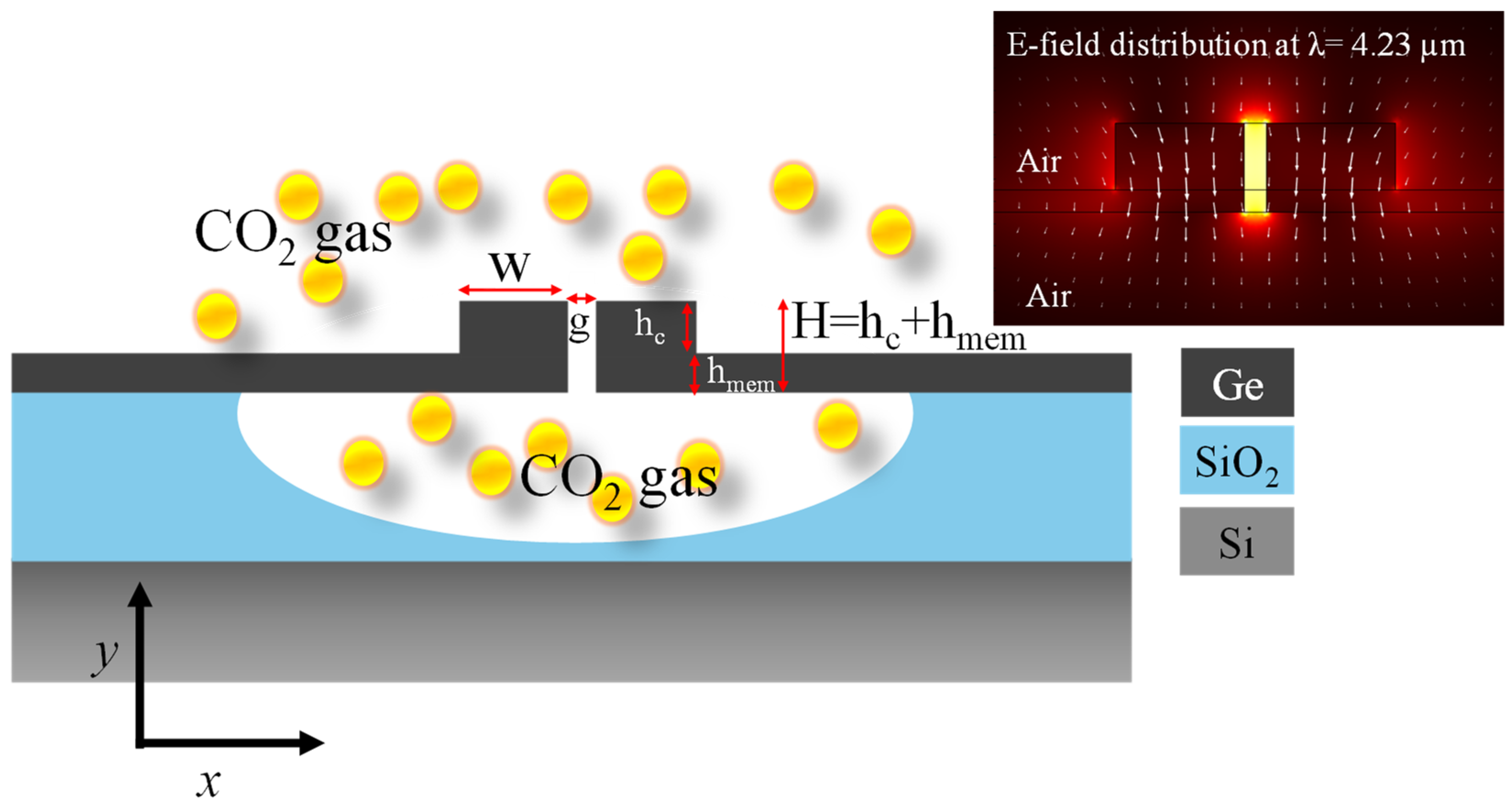
SSMW is an innovative structure for gas-sensing applications, characterized by its enhanced sensitivity and interplay with the target gas [36,37]. The waveguide features a narrow slot denoted as “g” that runs along its length, suspended in air or another low-index material, which significantly increases the overlap between the optical mode and the surrounding environment [38]. This design maximizes evanescent field exposure, allowing maximum light to interact with the gas molecules, thereby improving detection sensitivity. The width and height of the rails are represented by W and hcore, respectively. The rails are positioned on a suspended membrane of height (hmem), such that the total height (H) of the waveguide core is given by hcore + hmem. The graphical illustration of SSMW is shown in Figure 2.
The suspended nature of the membrane minimizes substrate losses and allows for high refractive index contrast, which enhances light confinement within the slot. In SSMW, the membrane is isolated from the substrate, making it more susceptible to mechanical deformations, such as bending or sagging, especially under external forces or thermal variations. An optimized membrane enhances the mechanical robustness, providing better resistance to these deformations, minimizing the αprop and sustaining the EM-field’s confinement in the narrow slot of the waveguide. This combination of increased light–gas interaction, low losses, and integration capability makes SSMW a powerful tool for precise and reliable gas-sensing applications [39,40,41]. The set of parameters that are used in the optimization process of the waveguide are presented in Table 1.
The finite-element method (FEM) utilized in COMSOL Multiphysics 6.0 is vital for examining SSMW’s modal characteristics, as it enables the precise handling of complex geometries and material variations. COMSOL provides extensive material property data, including the refractive index, through its built-in material libraries [42]. These libraries encompass a broad selection of predefined materials, each with associated physical properties such as refractive index, thermal conductivity, density, specific heat, and electrical conductivity. For waveguide design, materials like Ge, Si, and SiO2 are selected directly from these libraries. FEM divides the waveguide structure into smaller elements, offering a high level of spatial detail for the EM-field’s distribution. This approach facilitates the precise calculation of modal characteristics, including effective refractive indices, mode profiles, and loss parameters [43,44]. To calculate the effective refractive index (neff) of a waveguide, a simulation model of the structure is developed using COMSOL. The procedure begins with defining the geometry of the waveguide and assigning appropriate material properties to each region. COMSOL’s comprehensive material library offers predefined properties such as refractive index, thermal conductivity, and electrical conductivity, which can be assigned or customized as needed. The wave optic module then establishes the EM-wave equations that govern the system. Boundary conditions and initial parameters, including the incident light’s wavelength (typically 4.23 µm), are set. The model is subsequently meshed and solved to obtain the EM-field’s distribution. By analyzing these results, the real and imaginary components of neff are derived, typically through the propagation constant of the guided modes. This method enables the accurate characterization of the waveguide’s optical properties.

3. Evanescent Field Ratio and αprop of SSMW

The evanescent field ratio (EFR), also referred to as the penetration depth ratio, measures the relative strength of the evanescent field in comparison to the total field within an optical waveguide. In the case of SSMW, it is well defined as the ratio of the intensity or power of the evanescent field in the upper cladding (UC)+ nanogap (g)+ under-etched (UE) part to the total field intensity (rails + substrate + UC + g + UE), which is as follows:
E F R = U C + g + U E E ( x , y ) 2 d x d y r a i l s + s u b s t r a t e + U C + g + U E E ( x , y ) 2 d x d y ;
This parameter is vital for understanding the amount to which the evanescent field engages with its environment, directly influencing the sensitivity of different sensing applications. An increased EFR indicates a more significant interplay between the waveguide and its surroundings, making it ideal for sensing applications necessitating elevated sensitivity. Waveguide architectures are adjusted to accomplish the anticipated EFR by balancing factors such as waveguide geometry, material platform, αprop, and operating conditions, all aimed at enhancing sensing performance. Song et al. determined the EFR and αprop for various waveguide structures [33]. For the strip waveguide, the EFR was 0.15 with a propagation loss of 0.023 dB/cm. The subwavelength grating waveguide exhibited an EFR of 0.38 and a propagation loss of 1.54 dB/cm. The slot waveguide had an EFR of 0.47 and a propagation loss of 0.98 dB/cm, while the subwavelength grating slot waveguide showed an EFR of 0.56 with a propagation loss of 2.96 dB/cm.
The αprop in a waveguide can be quantitatively assessed by analyzing the imaginary part of the effective refractive index, denoted as Im(neff). The neff is a complex quantity, where the imaginary component represents the waveguide’s attenuation characteristics. Specifically, Im(neff) accounts for loss mechanisms such as absorption and scattering within the waveguide material. The αprop measured in dB/cm is related to this imaginary part through the following relationship:
α ( d B / c m ) = 4 × π × I m n e f f λ × 4.343
where λ is the wavelength of the propagating light. This formula indicates that a higher Im(neff) corresponds to greater attenuation per unit length.

4. Discussion

Enhanced evanescent fields play a crucial role in the realm of sensing technologies, offering significant advantages for various applications [45]. These fields, which occur at the interface between two media when light undergoes total internal reflection, are highly sensitive to changes in the local environment. The enhancement of the evanescent field typically achieved using specialized waveguides such as SSWG allows for the recognition of small variations in refractive index, molecular interactions, and the presence of specific analytes. This sensitivity makes enhanced evanescent fields particularly valuable for biochemical and medical sensing, where they can detect low concentrations of biomolecules, pathogens, or chemical substances with high precision [23].
In the first step, the waveguide geometry is optimized by keeping the nanoscale gap (g) and the membrane height (hmem) fixed at 100 nm. The Re(neff), αprop, and EFR are plotted as shown in Figure 3a, 3b, and 3c, respectively. During this process, W is varied between 400 nm and 800 nm, whereas hcore is varied between 200 nm and 300 nm, with a step size of 25 nm. The Re(neff) increases with an increase in both W and hcore, indicating that the EM-field is highly confined in the nanogap of the slot waveguide. For instance, when hcore is kept constant at 300 nm, the Re(neff) varies with changes in the W of the waveguide rail. Specifically, Re(neff) is 1.49 for W = 400 nm, 1.70 for W = 600 nm, and 2.03 for W = 800 nm. This trend demonstrates that, as the W of the waveguide rail increases, the Re(neff) also increases, further confirming the enhanced confinement of the EM-field within the nanogap and the rails of the slot waveguide. This relationship underscores the critical role of the waveguide width in tuning the optical properties of the device, which can be strategically utilized to achieve the desired performance characteristics in various photonic applications. Furthermore, the optimization of the waveguide dimensions aims to minimize αprop while maximizing neff, thereby improving the overall performance of the photonic device.
However, high modal confinement leads to a lower EFR attributable to the reduction in the evanescent field around the waveguide, as most of the power is confined within the nanoslot and high-index rail. For instance, the EFR values are approximately 0.86, 0.855, and 0.78 for W of 400 nm, 600 nm, and 800 nm, respectively, while keeping the hcore fixed at 300 nm, as revealed in Figure 3b. Moreover, the αprop of the waveguide is reciprocally related to the EFR value, as illustrated in Figure 3c. Specifically, the waveguide experiences a high αprop of 159.6 dB/cm when the EFR is around 0.86 for W = 400 nm and hcore = 300 nm. This signifies that W = 400 nm and hcore = 300 nm are highly undesirable geometric parameters, which lead to a lossy waveguide. In contrast, the αprop reduces to 0.001 dB/cm when W increases to 800 nm, with hcore remaining at 300 nm. This demonstrates that optimizing the waveguide dimensions can significantly reduce αprop, improving the overall performance of the waveguide.
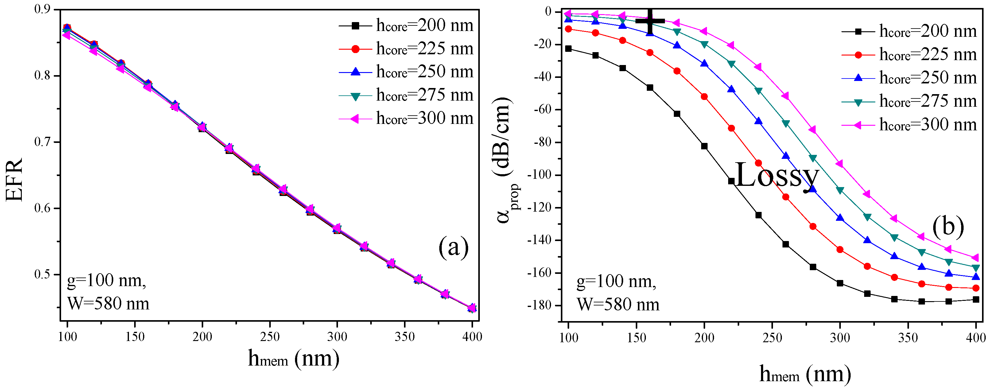
The optimized thickness (hmem) of the suspended membrane is critical for achieving an ultimate waveguide geometry in SSMWs. This optimization ensures that the waveguide can effectively confine the light in the nanogap and guide it with minimal loss, enhancing the interplay between the optical field and the surrounding environment. An appropriately chosen hmem balances mechanical stability with optical performance, leading to improved sensitivity and efficiency in applications such as sensing and signal processing. Consequently, the careful design and control of hmem are fundamental to the overall performance and functionality of SSMWs. In this analysis, g and W are fixed at 100 nm and 580 nm, respectively, while the EFR is calculated for varying values of hcore and hmem, as shown in Figure 4a. Note that, W = 580 nm is selected because it provides low αprop and high EFR, as estimated from Figure 3b,c.
It can be observed that the EFR declines as hmem surges from 100 nm to 400 nm. This is because the EM-field is significantly confined within the membrane and the waveguide rails rather than the nanoslot. Additionally, hcore has a minimum effect on the EFR. However, αprop is significantly high for hcore < 300 nm and hmem > 160 nm, as illustrated in Figure 4b. For hcore = 200 nm, the αprop ranges from 22.5 dB/cm to 46.3 dB/cm for hmem between 100 nm and 160 nm. This shows that hcore = 200 nm is not appropriate if a low αprop is required. For hcore = 300 nm, the αprop ranges from 1.07 to 3.86 dB/cm for hmem between 100 nm and 160 nm. However, hmem < 100 nm is quite low for the mechanical stability of the waveguide, and hmem> 160 nm introduces significant waveguide loss. Therefore, considering mechanical stability and αprop, the SSMW must be designed in such a way that hcore must be maintained at 300 nm and hmem can span between 100 nm and 160 nm.
Ultimately, the EFR and αprop of the SSMW are characterized as a function of varying hmem and g, as depicted in Figure 5a and Figure 5b, respectively. W and hcore are held constant at 580 nm and 300 nm, respectively. The EFR decreases as hmem increases from 100 nm to 400 nm, which can be attributed to the increasing confinement of the EM-field within the membrane and the rails. Interestingly, the parameter g exerts minimal influence on the EFR, offering flexibility in selecting g spanning 100–200 nm, as evidenced in Figure 5a. Conversely, optimizing the rail dimensions plays a crucial role in minimizing αprop for hmem values ranging between 100 nm and 400 nm. For instance, when g = 100nm, αprop is measured at 1.07 dB/cm, 1.48 dB/cm, 2.31 dB/cm, and 3.86 dB/cm for hmem of 100 nm, 120 nm, 140 nm, and 160 nm, respectively, as shown in Figure 5b. However, it is important to observe that EFR simultaneously decreases from 0.86 to 0.84, 0.81, and 0.78 as hmem increases from 100 nm to 120 nm, 140 nm, and 160 nm. This indicates the intrinsic trade-off between maximizing EFR and minimizing αprop.
The EFR and αprop for hmem spanning a range of 100 nm to 200 nm are detailed in Table 2. This table provides a comprehensive overview of both desirable and undesirable values of hmem, offering insights into the optimal thickness for specific applications. The data highlight the balance between maximizing performance and minimizing potential drawbacks, enabling a more informed selection of hmem values within the specified range. The SSMW structures with hmem values of 100–160 nm are favorable due to their ability to achieve high EFR values (0.78–0.86) while maintaining low αprop. Conversely, SSMW structures with hmem ≥ 100 nm are more prone to significant losses.
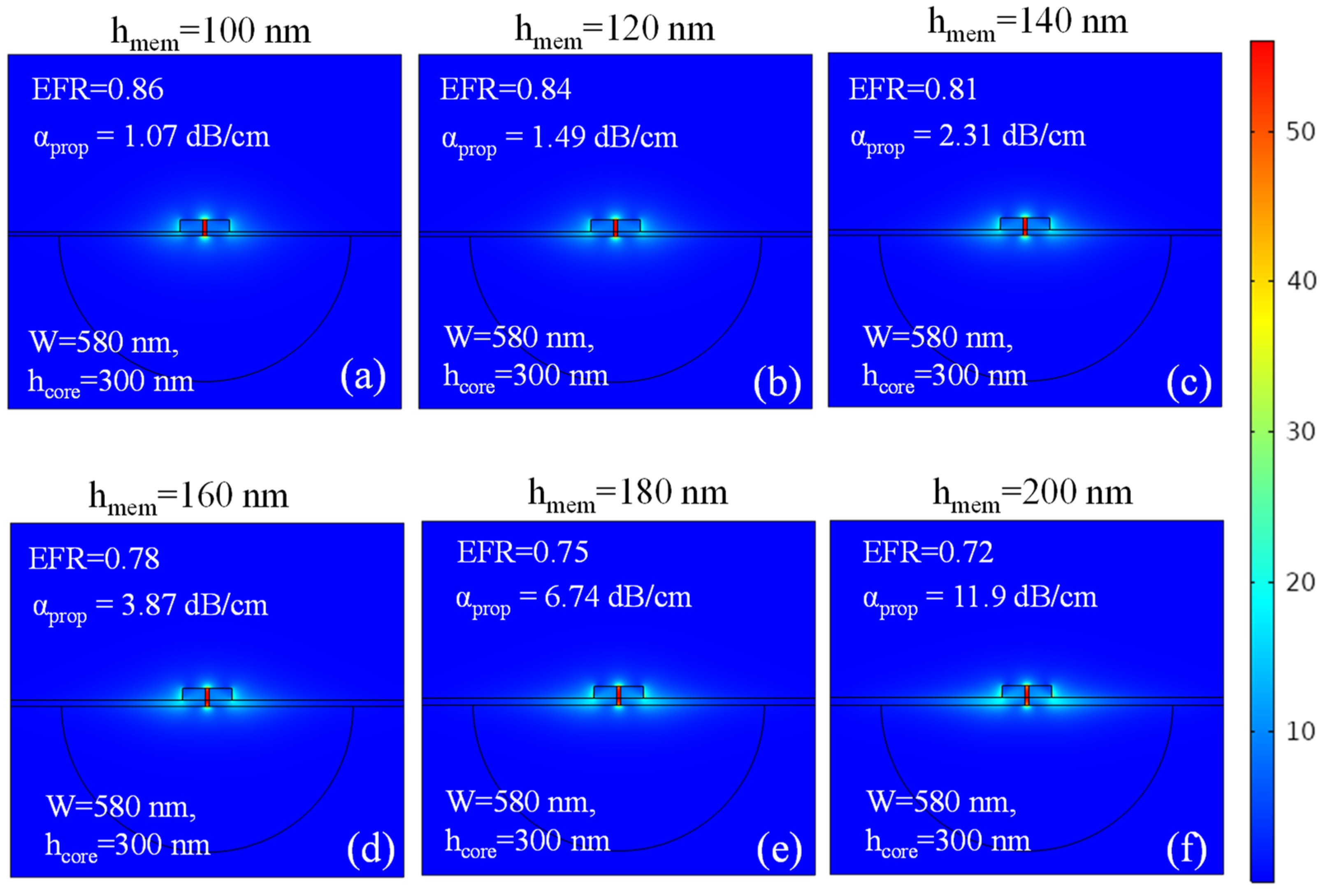
Figure 6a–f depict the normalized electric field profile within the SSMW at a wavelength of λ = 4.23 µm for varying hmem. The other geometric parameters—namely, W, hcore, and g—are held constant at 580 nm, 300 nm, and 100 nm, respectively. αprop exhibits a linear dependence on hmem, indicating that minimizing hmem is crucial for ensuring strict mode confinement within the nanoslot. If hmem is greater than the cut-off waveguide layer thickness, then the mode extends into the membrane, which consequently leads to an elevated αprop. Gehl et al. successfully demonstrated a suspended membrane waveguide (SMW) with hmem of 25 nm, 50 nm, and 75 nm, while maintaining the mechanical stability of the waveguide [40]. Therefore, we assume that, in the case of SSMW, hmem spanning the range of 100 nm to 160 nm can offer good mechanical stability; however, the sensitivity of the waveguide varies based on hmem, as explained in the next section.
The fabrication of SMWs typically involves several precise microfabrication techniques to create a thin, free-standing layer that supports light propagation. The process begins with a substrate, onto which a thin film of the desired waveguide material is deposited. Photolithography is then used to pattern the waveguide structure, followed by reactive ion etching (RIE) to define the waveguide and remove excess material [46]. To create the suspended membrane, a sacrificial layer is etched away, often using a selective wet or dry etching process, leaving the waveguide structure suspended above the substrate. The holes/patterns are created during the photolithography and etching steps to allow the chemical etchant to access and remove the sacrificial layer beneath the waveguide. The size and placement of these patterns are carefully designed to balance the need for efficient etching with the mechanical and optical integrity of the suspended waveguide.
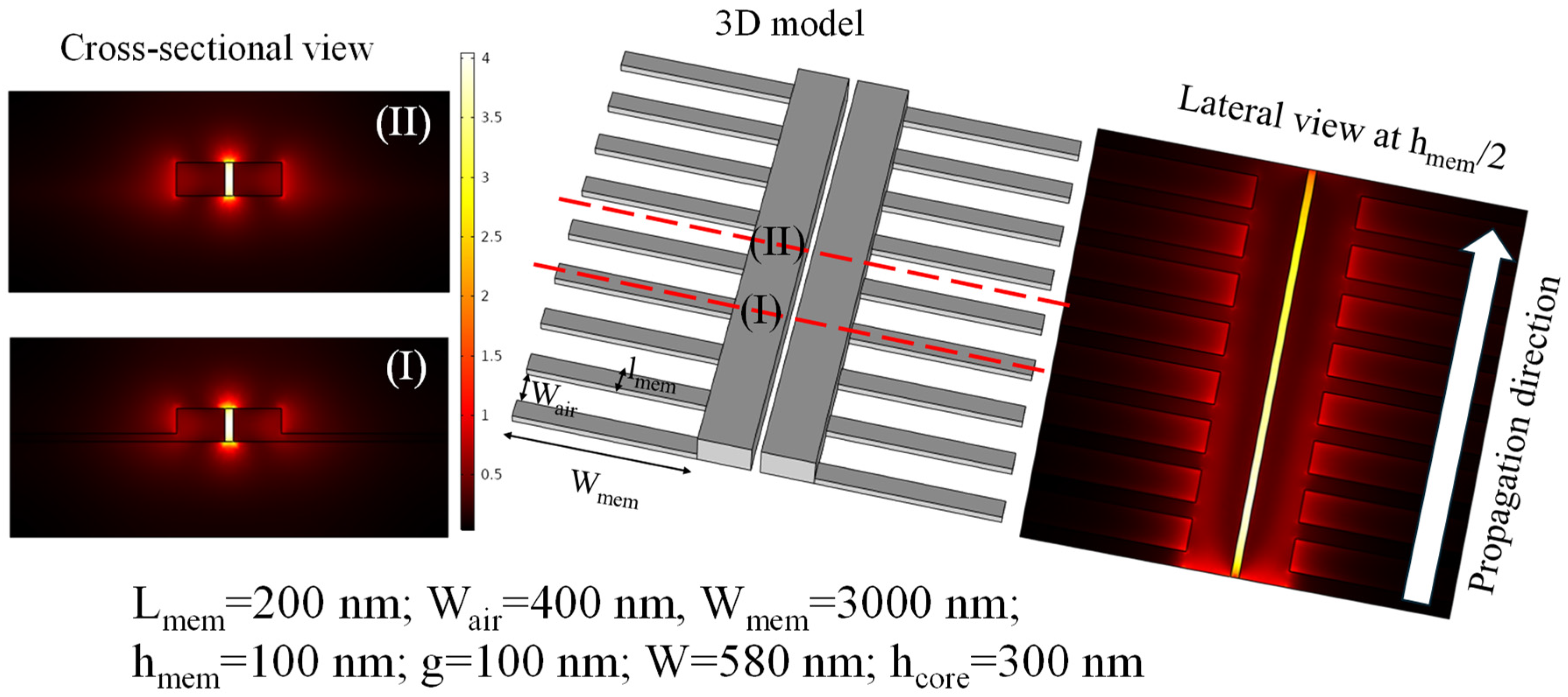
Qiao et al. designed an SMW utilizing a membrane width (lmem) of 200 nm and an air gap width (Wair) of 400 nm [46]. In this design, lmem refers to the width of the unetched membrane layer that forms the core of the waveguide, while Wair represents the width of the etched portion of the membrane, which creates a void or air gap beneath the suspended structure. This configuration is crucial for optimizing the optical confinement and minimizing losses in the waveguide. However, different values of lmem and Wair can also be used based on the optimization process. The 3D model of the SSMW is designed as shown in Figure 7 (middle). On the right-hand side, a lateral view of the normalized electric field profile within the SSMW taken at hmem/2 is depicted. This view demonstrates that the mode is well confined within the nanogap and effectively propagates along the waveguide. Additionally, the bottom-left panel presents a cross-sectional view of the normalized electric field profile within the unetched portion of the membrane, as indicated by the red dotted line (I). Meanwhile, the top-left panel shows the normalized electric field profile within the etched region of the membrane, marked by the red solid line (II). These visualizations highlight the distinct field distributions in both the unetched and etched sections of the waveguide, emphasizing the role of each region in mode confinement and propagation.

5. CO2 Gas Sensing

CO2 gas has multiple absorption windows ranging from the NIR to the MIR region. At a concentration of 1 ppm under conditions of 296 K and 1 atm, the absorption coefficient (ε) of CO2 molecules can reach up to 3.778 × 10⁻⁴ ppm·cm−1 at a wavelength of 4.23 μm [47,48], which is four to five orders of magnitude higher than that in the vicinity of the 1.57 μm region. Lambert–Beer’s law, also known as Beer’s law, is a fundamental principle used in gas sensing to quantify the concentration of a gas based on the attenuation of light as it passes through a sample. According to this law, the amount of light absorbed by a gas is directly proportional to the concentration of the gas and the path length of the light through the sample. By measuring the decrease in light intensity at specific wavelengths, gas sensors can accurately determine the concentration of various gasses in a mixture. Based on Lambert–Beer’s law, the sensitivity of the SSMW is calculated using the following expression:
S e n s i t i v i t y = d ( I / I o ) d ( c ) = η ε L exp η ε C L α p r o p L = η ε L I n ;
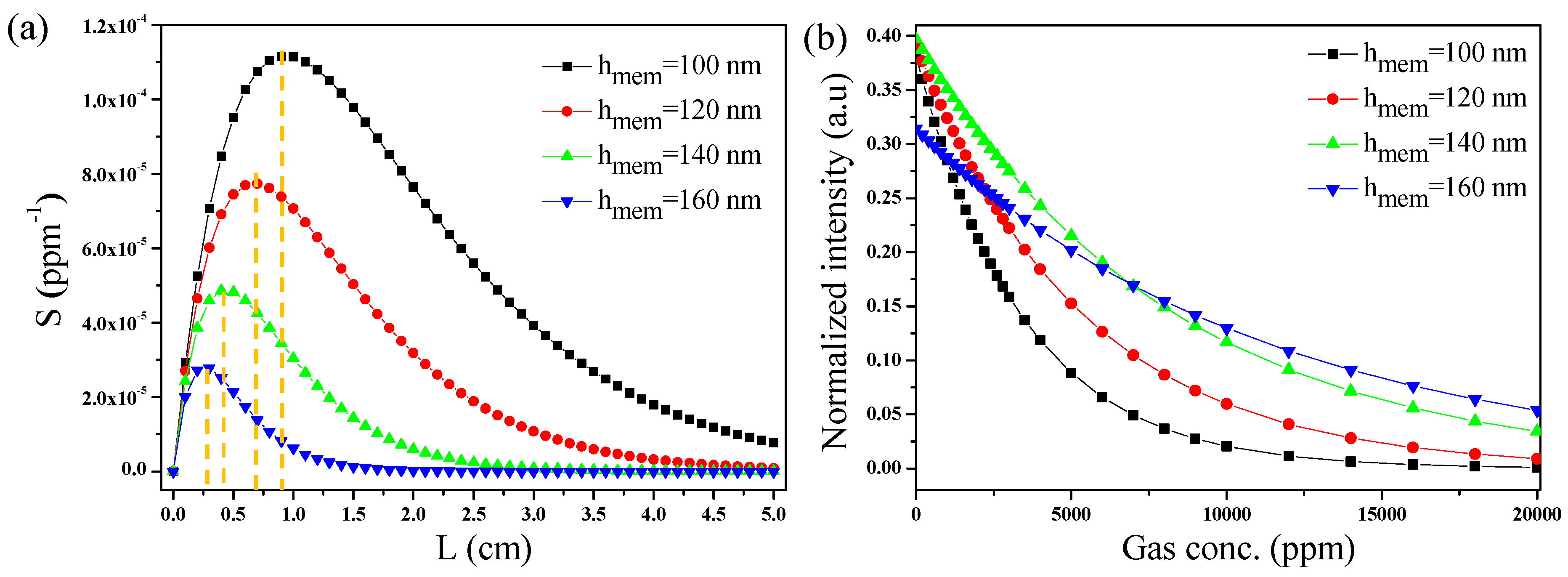
A minus sign in the equation indicates the absorption phenomenon, while In = I/Io represents the normalized intensity of the output light proportionate to the input light. Sensitivity is influenced by factors such as L and αprop, as well as η. These factors are critical for determining the sensitivity of the transducer. By differentiating both sides of Equation (3), it is determined that the sensitivity achieves its maximum value when L is set to 1/(ηεC + αprop). Figure 8a presents the sensitivity of an SSMW versus the L. From Table 2, it is evident that η decreases and αprop increases as hmem increases from 100 nm to 200 nm. This explains why sensitivity decreases as the waveguide length (L) increases, primarily due to the associated rise in total propagation losses. Additionally, hmem significantly impacts the device’s sensitivity, with αprop being higher for hmem = 160 nm compared to hmem = 100 nm. Consequently, it is crucial to optimize the waveguide’s geometric parameters to achieve maximum sensitivity. Fine-tuning these dimensions allows for a balance between minimizing propagation loss and enhancing light–matter interaction, leading to the most effective performance of the gas-sensing device. Table 3 summarizes the optimized lengths of SSMW for different values of hmem, where maximum sensitivity is obtained. This signifies that the sensitivity obtained by SSMW is significantly higher than the ones reported for subwavelength grating slots and slot waveguides that can reach up to 2.60 × 10⁻⁵ ppm−1 and 6.66 × 10⁻⁵ ppm−1 [33].
The normalized intensity (In) is plotted against the different concentrations of CO2 gas using Equation (4):
I n = exp η ε C L o p t α p r o p L o p t ;
The light propagating in the SSMW with hmem of 100 nm decays more rapidly when exposed to CO2 gas compared to waveguide configurations with hmem values of 120 nm, 140 nm, and 160 nm, as illustrated in Figure 8b. This is because η and Lopt obtained at hmem = 100 nm are greater than other values of hmem, i.e., 0.86 and 0.9 cm, respectively (see Table 3). Moreover, with αprop as low as 1.07 dB/cm, the waveguide exhibits a relatively longer interaction length, thereby enhancing its sensitivity and resulting in a faster decay of output power compared to the values reported for slot waveguides and subwavelength grating slot waveguides [33].

6. Conclusions

An SSMW based on Ge-on-SOI is highly advantageous for gas sensing in the MIR wavelength range. The MIR region is predominantly important for gas sensing because several gasses exhibit strong absorption features in this range. The high refractive index of Ge enables the tight confinement of light within the waveguide, enhancing light–matter interactions and enhancing the sensitivity of the sensor to trace gas concentrations. The suspended design minimizes optical losses by reducing the interaction with the substrate, thus improving the overall sensing performance. In this work, the SSMW is optimized at an operational wavelength of 4.23 µm, which links the absorption line of CO2 gas. Our optimized waveguide geometry exhibits an exceptional EFR of 0.86, combined with an impressively low propagation loss of just 1.07 dB/cm. This advanced design delivers outstanding sensitivity, reaching 1.12 × 10⁻⁴ ppm−1 for a waveguide length of only 0.9 cm, underscoring its potential for precision in MIR sensing applications.
Since the sensing mechanism is purely physical (based on optical absorption) and does not involve chemical binding or adsorption of CO2 molecules to the waveguide surface, the sensor offers excellent reusability. The interaction is non-invasive, and no permanent changes or degradation of the waveguide occur during operation. Therefore, the proposed structure can be reused indefinitely without performance loss, provided that the waveguide and optical setup are maintained properly. The insights gained from this research pave the way for the development of next-generation sensors capable of detecting trace gas concentrations with unparalleled accuracy, thus playing a vital role in addressing global environmental challenges.

Author Contributions

Conceptualization, M.A.B. and R.P.; methodology, M.A.B.; software, M.A.B.; validation, M.A.B. and R.P.; formal analysis, M.A.B.; investigation, M.A.B.; resources, R.P.; data curation, M.A.B.; writing—original draft preparation, M.A.B.; writing—review and editing, M.A.B. and R.P.; visualization, M.A.B.; supervision, R.P.; project administration, R.P.; and funding acquisition, M.A.B. All authors have read and agreed to the published version of the manuscript.

Funding

This research received no external funding.

Data Availability Statement

Data will be available upon reasonable request.

Acknowledgments

The authors acknowledge the constant support of the Warsaw University of Technology toward completion of this work.

Conflicts of Interest

The authors declare no conflicts of interest.

References

  1. Harivelo, R.Z.M.; Harifidy, R.Z. A Review of Environmental Protection and Sustainable Development in Madagascar. J 2022, 5, 512–531. [Google Scholar] [CrossRef]
  2. Wu, L.; Qing, C.; Jin, S. Environmental Protection and Sustainable Development of Enterprises in China: The Moderating Role of Media Attention. Front. Environ. Sci. 2022, 10, 966479. [Google Scholar] [CrossRef]
  3. Wentworth, A. As Climate Disasters Grow, Early Warning Systems Become Essential. Available online: https://www.climatechangenews.com/2023/12/08/as-climate-disasters-grow-early-warning-systems-become-essential/ (accessed on 24 August 2024).
  4. Dai, D.; Zhou, B.; Zhao, S.; Li, K.; Liu, Y. Research on Industrial Carbon Emission Prediction and Resistance Analysis Based on CEI-EGM-RM Method: A Case Study of Bengbu. Sci. Rep. 2023, 13, 14528. [Google Scholar] [CrossRef] [PubMed]
  5. Permentier, K.; Vercammen, S.; Soetaert, S.; Schellemans, C. Carbon Dioxide Poisoning: A Literature Review of an Often Forgotten Cause of Intoxication in the Emergency Department. Int. J. Emerg. Med. 2017, 10, 14. [Google Scholar] [CrossRef] [PubMed]
  6. Jacobson, T.A.; Kler, J.S.; Hernke, M.T.; Braun, R.K.; Meyer, K.C.; Funk, W.E. Direct Human Health Risks of Increased Atmospheric Carbon Dioxide. Nat. Sustain. 2019, 2, 691–701. [Google Scholar] [CrossRef]
  7. Duarte, C.M.; Jaremko, Ł.; Jaremko, M. Hypothesis: Potentially Systemic Impacts of Elevated CO2 on the Human Proteome and Health. Front. Public Health 2020, 8, 543322. [Google Scholar] [CrossRef]
  8. Eldesouki, M.H.; Rashed, A.E.; El-Moneim, A.A. A Comprehensive Overview of Carbon Dioxide, Including Emission Sources, Capture Technologies, and the Conversion into Value-Added Products. Clean Technol. Environ. Policy 2023, 25, 3131–3148. [Google Scholar] [CrossRef]
  9. Baldacci, A.; Malathy Devi, V.; Chen, D.-W.; Narahari Rao, K.; Fridovich, B. Absorption Spectrum of Carbon Dioxide at 4.3 Μm. J. Mol. Spectrosc. 1978, 70, 143–159. [Google Scholar] [CrossRef]
  10. Wei, P.-S.; Hsieh, Y.-C.; Chiu, H.-H.; Yen, D.-L.; Lee, C.; Tsai, Y.-C.; Ting, T.-C. Absorption Coefficient of Carbon Dioxide across Atmospheric Troposphere Layer. Heliyon 2018, 4, e00785. [Google Scholar] [CrossRef]
  11. Ottonello-Briano, F.; Errando-Herranz, C.; Rödjegård, H.; Martin, H.; Sohlström, H.; Gylfason, K.B. Carbon Dioxide Absorption Spectroscopy with a Mid-Infrared Silicon Photonic Waveguide. Opt. Lett. OL 2020, 45, 109–112. [Google Scholar] [CrossRef]
  12. Romaniello, V.; Spinetti, C.; Silvestri, M.; Buongiorno, M.F. A Sensitivity Study of the 4.8 Μm Carbon Dioxide Absorption Band in the MWIR Spectral Range. Remote Sens. 2020, 12, 172. [Google Scholar] [CrossRef]
  13. Nedeljkovic, M.; Penades, J.S.; Mittal, V.; Murugan, G.S.; Khokhar, A.Z.; Littlejohns, C.; Carpenter, L.G.; Gawith, C.B.E.; Wilkinson, J.S.; Mashanovich, G.Z. Germanium-on-Silicon Waveguides Operating at Mid-Infrared Wavelengths up to 8.5 Μm. Opt. Express OE 2017, 25, 27431–27441. [Google Scholar] [CrossRef] [PubMed]
  14. Lim, J.; Shim, J.; Geum, D.-M.; Kim, S. Experimental Demonstration of Germanium-on-Silicon Slot Waveguides at Mid-Infrared Wavelength. IEEE Photonics J. 2022, 14, 1–9. [Google Scholar] [CrossRef]
  15. Yeh, P.-L.; Wu, B.-R.; Peng, Y.-W.; Wu, C.-W.; Jheng, Y.-T.; Lee, K.H.; Chen, Q.; Tan, C.S.; Chang, G.-E. Defect-Engineered Electrically-Injected Germanium-on-Insulator Waveguide Light Emitters at Telecom Wavelengths. Adv. Electron. Mater. 2023, 9, 2300288. [Google Scholar] [CrossRef]
  16. Kozak, D.A.; Tyndall, N.F.; Pruessner, M.W.; Rabinovich, W.S.; Stievater, T.H. Germanium-on-Silicon Waveguides for Long-Wave Integrated Photonics: Ring Resonance and Thermo-Optics. Opt. Express OE 2021, 29, 15443–15451. [Google Scholar] [CrossRef]
  17. Li, W.; Anantha, P.; Bao, S.; Lee, K.H.; Guo, X.; Hu, T.; Zhang, L.; Wang, H.; Soref, R.; Tan, C.S. Germanium-on-Silicon Nitride Waveguides for Mid-Infrared Integrated Photonics. Appl. Phys. Lett. 2016, 109, 241101. [Google Scholar] [CrossRef]
  18. Butt, M.A.; Kazanskiy, N.L.; Khonina, S.N.; Voronkov, G.S.; Grakhova, E.P.; Kutluyarov, R.V. A Review on Photonic Sensing Technologies: Status and Outlook. Biosensors 2023, 13, 568. [Google Scholar] [CrossRef]
  19. Butt, M.A.; Mateos, X.; Piramidowicz, R. Photonics Sensors: A Perspective on Current Advancements, Emerging Challenges, and Potential Solutions (Invited). Phys. Lett. A 2024, 516, 129633. [Google Scholar] [CrossRef]
  20. Butt, M.A.; Piramidowicz, R. Integrated Photonic Sensors for the Detection of Toxic Gasses—A Review. Chemosensors 2024, 12, 143. [Google Scholar] [CrossRef]
  21. Butt, M.A.; Voronkov, G.S.; Grakhova, E.P.; Kutluyarov, R.V.; Kazanskiy, N.L.; Khonina, S.N. Environmental Monitoring: A Comprehensive Review on Optical Waveguide and Fiber-Based Sensors. Biosensors 2022, 12, 1038. [Google Scholar] [CrossRef]
  22. Anjana, N.S.; Amarnath, A.; Harindranathan Nair, M.V. Toxic Hazards of Ammonia Release and Population Vulnerability Assessment Using Geographical Information System. J. Environ. Manag. 2018, 210, 201–209. [Google Scholar] [CrossRef] [PubMed]
  23. Butt, M.A.; Degtyarev, S.A.; Khonina, S.N.; Kazanskiy, N.L. An Evanescent Field Absorption Gas Sensor at Mid-IR 3.39 Μm Wavelength. J. Mod. Opt. 2017, 64, 1892–1897. [Google Scholar] [CrossRef]
  24. Kazanskiy, N.L.; Khonina, S.N.; Butt, M.A. Polarization-Insensitive Hybrid Plasmonic Waveguide Design for Evanescent Field Absorption Gas Sensor. Photonic Sens. 2021, 11, 279–290. [Google Scholar] [CrossRef]
  25. Butt, M.A. Analyzing the Evanescent Field Ratio of Ridge Waveguide Based on Different Material Platforms for Sensing Applications. J. Opt. 2024, 26, 095803. [Google Scholar] [CrossRef]
  26. Joshi, K.; Meena, B.L.; Gehlot, K. Performance of Silicon-on-Insulator and Silicon-on-Sapphire Based Evanescent Field Gas Sensor Operating at 2.86 Μm. AIP Conf. Proc. 2023, 2768, 020023. [Google Scholar] [CrossRef]
  27. Tang, X.; Li, Y.; Chen, F.; Yang, W. Gas Concentration and Refractive Index Sensor Based on Plasmonic Induced Absorption in Metal-Insulator-Metal Waveguide Coupled with Arc Resonators Structure. Phys. Scr. 2024, 99, 065561. [Google Scholar] [CrossRef]
  28. Wamg, G.; Shi, Q.; Chen, F.; Yu, Y. Gas Sensor Based on Multiple Fano Resonances in Metal-Insulator-Metal Waveguide Resonator System. J. Optoelectron. Adv. Mater. 2022, 24, 323–331. [Google Scholar]
  29. Khonina, S.N.; Kazanskiy, N.L.; Butt, M.A.; Kaźmierczak, A.; Piramidowicz, R. Plasmonic Sensor Based on Metal-Insulator-Metal Waveguide Square Ring Cavity Filled with Functional Material for the Detection of CO2 Gas. Opt. Express OE 2021, 29, 16584–16594. [Google Scholar] [CrossRef]
  30. Stewart, G.; Jin, W.; Culshaw, B. Prospects for Fibre-Optic Evanescent-Field Gas Sensors Using Absorption in the near-Infrared. Sens. Actuators B Chem. 1997, 38, 42–47. [Google Scholar] [CrossRef]
  31. Vlk, M.; Datta, A.; Alberti, S.; Yallew, H.D.; Mittal, V.; Murugan, G.S.; Jágerská, J. Extraordinary Evanescent Field Confinement Waveguide Sensor for Mid-Infrared Trace Gas Spectroscopy. Light Sci. Appl. 2021, 10, 26. [Google Scholar] [CrossRef]
  32. Ranacher, C.; Consani, C.; Hedenig, U.; Grille, T.; Lavchiev, V.; Jakoby, B. A Photonic Silicon Waveguide Gas Sensor Using Evanescent-Wave Absorption. In Proceedings of the 2016 IEEE Sensors, Orlando, FL, USA, 30 October–3 November 2016; pp. 1–3. [Google Scholar]
  33. Song, Y.; Li, B.; Zhang, H.; Li, M.; Li, Q.; He, J.-J. Silicon Waveguide Sensors for Carbon Dioxide Gas Sensing in the Mid-Infrared Region. Photonics 2023, 10, 120. [Google Scholar] [CrossRef]
  34. Butt, M.A.; Piramidowicz, R. Standard Slot Waveguide and Double Hybrid Plasmonic Waveguide Configurations for Enhanced Evanescent Field Absorption Methane Gas Sensing. Photonics Lett. Pol. 2022, 14, 10–12. [Google Scholar] [CrossRef]
  35. Ranacher, C.; Consani, C.; Vollert, N.; Tortschanoff, A.; Bergmeister, M.; Grille, T.; Jakoby, B. Characterization of Evanescent Field Gas Sensor Structures Based on Silicon Photonics. IEEE Photonics J. 2018, 10, 1–14. [Google Scholar] [CrossRef]
  36. Butt, M.A.; Kazansky, N.L. SOI Suspended Membrane Waveguide at 3.39 Μm for Gas Sensing Application. Photonics Lett. Pol. 2020, 12, 67–69. [Google Scholar] [CrossRef]
  37. Zhou, W.; Cheng, Z.; Wu, X.; Zhu, B.; Sun, X.; Tsang, H.K. Fully Suspended Slot Waveguides for High Refractive Index Sensitivity. Opt. Lett. OL 2017, 42, 1245–1248. [Google Scholar] [CrossRef]
  38. Zhou, W.; Cheng, Z.; Wu, X.; Sun, X.; Tsang, H.K. Fully Suspended Slot Waveguide Platform. J. Appl. Phys. 2018, 123, 063103. [Google Scholar] [CrossRef]
  39. Kazanskiy, N.L.; Butt, M.A.; Khonina, S.N. Silicon Photonic Devices Realized on Refractive Index Engineered Subwavelength Grating Waveguides-A Review. Opt. Laser Technol. 2021, 138, 106863. [Google Scholar] [CrossRef]
  40. Gehl, M.; Kindel, W.; Karl, N.; Orozco, A.; Musick, K.; Trotter, D.; Dallo, C.; Starbuck, A.; Leenheer, A.; DeRose, C.; et al. Characterization of Suspended Membrane Waveguides towards a Photonic Atom Trap Integrated Platform. Opt. Express OE 2021, 29, 13129–13140. [Google Scholar] [CrossRef]
  41. Bian, D.; Lei, X.; Chen, S. Dispersion Characteristics of Nanometer-Scaled Silicon Nitride Suspended Membrane Waveguides. J. Semicond. 2016, 37, 114007. [Google Scholar] [CrossRef]
  42. Comprehensive Material Library with over 15,000 Materials. Available online: https://www.comsol.com/material-library (accessed on 23 August 2024).
  43. Hoang, T.; Duhamel, D.; Foret, G. Wave Finite Element Method for Waveguides and Periodic Structures Subjected to Arbitrary Loads. Finite Elem. Anal. Des. 2020, 179, 103437. [Google Scholar] [CrossRef]
  44. Koshiba, M. Optical Waveguide Theory by the Finite Element Method. IEICE Trans. Electron. 2014, E97C, 625–635. [Google Scholar] [CrossRef]
  45. Butt, M.A. Dielectric Waveguide-Based Sensors with Enhanced Evanescent Field: Unveiling the Dynamic Interaction with the Ambient Medium for Biosensing and Gas-Sensing Applications—A Review. Photonics 2024, 11, 198. [Google Scholar] [CrossRef]
  46. Qiao, Q.; Sun, H.; Liu, X.; Dong, B.; Xia, J.; Lee, C.; Zhou, G. Suspended Silicon Waveguide with Sub-Wavelength Grating Cladding for Optical MEMS in Mid-Infrared. Micromachines 2021, 12, 1311. [Google Scholar] [CrossRef] [PubMed]
  47. Rothman, L.S.; Jacquemart, D.; Barbe, A.; Chris Benner, D.; Birk, M.; Brown, L.R.; Carleer, M.R.; Chackerian, C.; Chance, K.; Coudert, L.H.; et al. The HITRAN 2004 Molecular Spectroscopic Database. J. Quant. Spectrosc. Radiat. Transf. 2005, 96, 139–204. [Google Scholar] [CrossRef]
  48. Hill, C.; Gordon, I.E.; Kochanov, R.V.; Barrett, L.; Wilzewski, J.S.; Rothman, L.S. HITRANOnline: An Online Interface and the Flexible Representation of Spectroscopic Data in the HITRAN Database. J. Quant. Spectrosc. Radiat. Transf. 2016, 177, 4–14. [Google Scholar] [CrossRef]
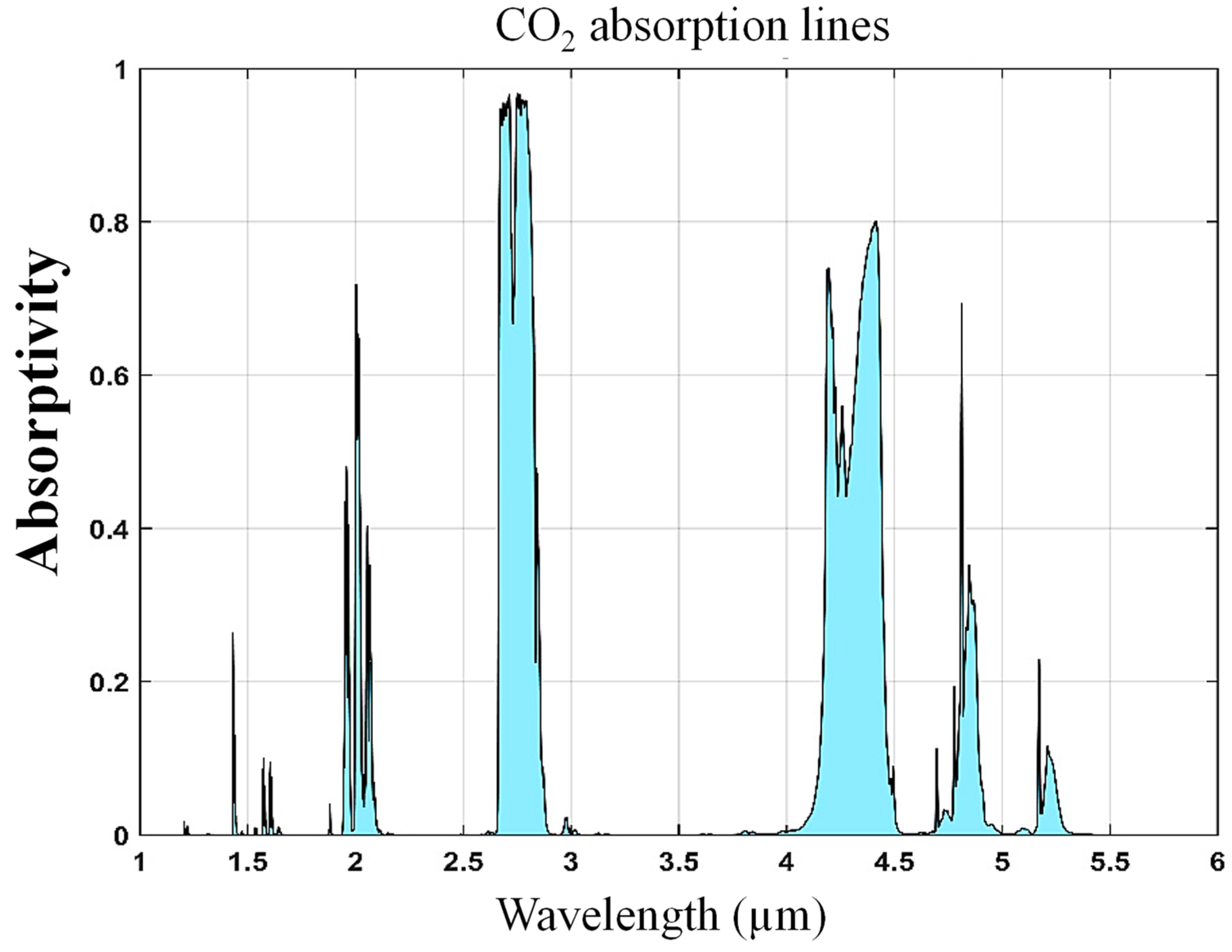
Figure 1. CO2 absorption bands in the SWIR–MWIR spectral range [12].
Micromachines 15 01434 g001
Figure 2. Schematic depiction of a Ge-on-SOI platform-based SSMW. Inset: normalized electric field distribution at λ = 4.23 µm.
Micromachines 15 01434 g002
Figure 3. (a) Re(neff) versus W, (b) EFR versus W, and (c) loss versus W.
Micromachines 15 01434 g003
Figure 4. (a) EFR versus hmem and hcore, and (b) αprop versus hmem and hcore. W and g are kept constant at 580 nm and 100 nm, respectively. The black cross in (b) represents the waveguide geometry (hcore = 300 nm and hmem = 160 nm) where αprop is significantly low.
Micromachines 15 01434 g004
Figure 5. (a) EFR versus hmem and g, and (b) αprop versus hmem and g. W and hcore are kept constant at 580 nm and 300 nm, respectively.
Micromachines 15 01434 g005
Figure 6. Normalized electric field profile in the SSMW of W = 580 nm, hcore = 300 nm, and g = 100 nm, whereas hmem varies to (a) 100 nm, (b) 120 nm, (c) 140 nm, (d) 160 nm, (e) 180 nm, and (f) 200 nm.
Micromachines 15 01434 g006
Figure 7. The three-dimensional model of the SSMW is in the (middle). The right side presents the lateral view of the normalized electric field profile in the waveguide at hmem/2. The cross-sectional view of the electric field profile is shown: (top-left) etched part of the membrane; and (bottom-left) unetched part of the membrane.
Micromachines 15 01434 g007
Figure 8. (a) Sensitivity of the SSMW versus L and (b) normalized intensity versus gas concentration.
Micromachines 15 01434 g008
Table 1. Geometric parameters used in modeling.
VariableExpressionRange (nm)
WWidth of the waveguide rail400–800
gNanogap100–200
hmemThickness of the membrane100–400
hcoreThickness of the waveguide core200–300
HTotal height (hc + hmem)300–700
Table 2. Characteristics of SSMW based on hmem. The results are extracted from Figure 5.
g = 100 nm
hmem (nm)EFRαprop (dB/cm)Remarks
1000.861.07Highly desirable
1200.831.49Highly desirable
1400.812.31Highly desirable
1600.783.86Desirable
1800.756.74Least desirable
2000.7211.88Lossy
Table 3. The sensitivity of the SSMW versus L. hmem has a big influence on the waveguide sensitivity.
hmem (nm)Lopt (cm)Sensitivity (ppm−1)
1000.91.12 × 10−4
1200.67.69 × 10−5
1400.44.85 × 10−5
1600.32.77 × 10−5
Disclaimer/Publisher’s Note: The statements, opinions and data contained in all publications are solely those of the individual author(s) and contributor(s) and not of MDPI and/or the editor(s). MDPI and/or the editor(s) disclaim responsibility for any injury to people or property resulting from any ideas, methods, instructions or products referred to in the content.